Note: Descriptions are shown in the official language in which they were submitted.
MULTI-ZONE EC WINDOWS
CROSS-REFERENCES TO RELATED APPLICATIONS
[00011
FIELD
[0002] Embodiments disclosed herein relate generally to optical devices, and
more
particularly to methods of fabricating optical devices and particularly to
electrochromic (EC)
windows having multiple tinting zones.
BACKGROUND
[00031 Electrochromism is a phenomenon in which a maim ial eAhibits a
tevcisible
electrochemically-mediated change in an optical property when placed in a
different
electronic state, typically by being subjected to a voltage change. The
optical property is
typically one or more of tint, transmittance, absorbance, and reflectance. For
example, one
well known electrochrornie material is tungsten oxide (W03). Tungsten oxide is
a
cathodically tinting electrochromic material in which a tinting transition,
bleached (untinted)
to blue, occurs by electrochemical reduction. When electrochemical oxidation
takes place,
tungsten oxide transitions from blue to a bleached state.
[0004] Electrochromic materials may be incorporated into, for example, windows
for home,
commercial and other uses. The tint, transmittance, absorbance, and/or
reflectance of such
windows may be changed by inducing a change in the electiochromic material,
that is,
electrochromic windows are windows that can be darkened and lightened
reversibly via
application of an electric charge. A small voltage applied to an
electrochromic device of the
window will cause it to darken; reversing the voltage causes it to lighten.
This capability
allows control of the amount of light that passes through the windows, and
presents an
opportunity for electrochromic windows to be used as energy-saving devices.
1
CA 2890749 2018-11-07
[0005] While electrochromism was discovered in the 1960s, electrochromic
devices, and
particularly electrochromic windows, still unfortunately suffer various
problems and have not
begun to realize their full commercial potential despite much recent
advancement in
electrochromic technology, apparatus, and related methods of making and/or
using
electrochromic devices.
SUMMARY"
[0006] Thin-film devices, for example, electrochromic devices for windows, and
methods of
manufacturing are described. Embodiments include electrochromic window lites
having two
or more tinting (or coloration) zones, where there is only a single monolithic
electrochromic
device on the lite. The tinting zones are defined by virtue of the means for
applying potential
to the device and/or by a resistive zone between adjacent tinting zones. For
example, sets of
bus bars are configured to apply potential across separate zones (areas) of
the device and
thereby tint them selectively. The advantages include no visible scribe lines
in the viewable
area of the EC window due to cutting through the EC device to make separate
devices that
serve as tinting zones.
[0007] One embodiment is an electrochromic window lite including a monolithic
EC device
on a transparent substrate, the monolithic EC device including two or more
tinting zones,
each of said two or more tinting zones configured for operation independent of
the others and
each having its own associated bus bars, where the two or more tinting zones
are not
separated from each other by isolation scribes. That is, the EC device stack
is not cut
through, but rather is intact as a monolithic device. For example, there may
be two tinting
zones on the lite and the associated bus bars arranged are located at opposing
edges of the lite
(e.g., vertically oriented), wherein a set of bus bars is associated with each
of the two tinting
zones.
According to an aspect of the present invention, there is provided an
electrochromic
(EC) window lite comprising:
a monolithic EC device disposed on a transparent substrate, the monolithic EC
device
comprising first and second transparent conductor layers and an EC stack
between the first
and second transparent conductor layers; and
a resistive zone in one of the first and second transparent conducting layers,
2
CA 2890749 2018-11-07
wherein the resistive zone has a higher electrical resistance than a portion
of the one of
the first and second transparent conducting layers outside the resistive zone.
According to another aspect of the present invention, there is provided an
electrochromic (EC) window lite comprising:
a monolithic EC device on a transparent substrate; and
at least one pair of lengthwise variable bus bars configured to produce a tint
gradient
zone on the monolithic EC device when energized.
According to another aspect of the present invention, there is provided an
electrochromic window lite comprising:
a monolithic EC device disposed on a transparent substrate, the monolithic EC
device
comprising first and second transparent conductor layers and an EC stack
between the first and
second transparent conductor layers; and
a resistive zone in one of the first and second transparent conducting layers,
wherein the resistive zone has a higher electrical resistance than a portion
of the one of
the first and second transparent conducting layers outside the resistive zone,
and wherein the
resistive zone is configured to tint.
According to another aspect of the present invention, there is provided an
electrochromic window lite comprising:
a monolithic EC device on a transparent substrate; and
at least one pair of bus bars, each bus bar having variable electrical
resistance along its
length and configured to produce a tint gradient zone on the monolithic EC
device when
energized, each pair of bus bars located continuously along opposing edges of
the
electrochromic device, each bus bar configured to apply a lengthwise voltage
gradient along a
respective opposing edge when energized, wherein the tint gradient is in a
direction along a
length of the bus bars.
According to a further aspect of the present invention, there is provided an
electrochromic window lite comprising:
a monolithic EC device on a transparent substrate, the monolithic EC device
having a
top and a bottom; and
2a
Date Recue/Date Received 2021-12-06
one or more pair of bus bars located continuously along opposing edges of the
electrochromic device and configured to produce a tint gradient between the
top and the
bottom of the monolithic EC device when energized,
wherein the tint gradient is darker at the top than at the bottom or darker at
the bottom
.. than at the top.
According to another aspect of the present invention, there is provided an
electrochromic window lite comprising:
a monolithic EC device on a transparent substrate, the monolithic EC device
having a
top and a bottom; and
one or more pair of bus bars located continuously along opposing edges of the
electrochromic device and configured to produce a top down tint gradient
between the top and
the bottom of the monolithic EC device when energized.
According to a further aspect of the present invention, there is provided an
electrochromic window lite comprising:
a monolithic EC device on a transparent substrate, the monolithic EC device
having a
top and a bottom; and
one or more pair of bus bars located continuously along opposing edges of the
electrochromic device and configured to produce a bottom up tint gradient
between the top and
the bottom of the monolithic EC device when energized.
According to another aspect of the present invention, there is provided an
electrochromic window comprising:
an electrochromic device disposed on a transparent substrate, the
electrochromic device
comprising a first transparent conductive oxide layer and a second transparent
conductive
oxide layer;
one or more material layers sandwiched between the first and second
transparent
conductor layers; and
a pair of bus bars located continuously along opposing edges of the
electrochromic
device, one of the pair of bus bars in electrical communication with the first
transparent
conductive oxide layer and the other of the pair of bus bars in electrical
communication with
the second transparent conductive oxide layer;
2b
Date Recue/Date Received 2021-07-08
wherein each bus bar of the pair of bus bars is configured to apply a
lengthwise voltage
gradient along a respective opposing edge when energized.
According to a further aspect of the present invention, there is provided an
electrochromic window lite comprising:
a monolithic electrochromic device on a transparent substrate; and
at least one pair of bus bars configured to produce a tint gradient across the
monolithic
electrochromic device when energized, each pair of bus bars located
continuously along
opposing edges of the electrochromic device, each bus bar configured to apply
a lengthwise
voltage gradient along a respective opposing edge when energized, wherein the
tint gradient is
in a direction along a length of the bus bars.
According to a further aspect of the present invention, there is provided an
electrochromic device comprising:
a first bus bar electrically connected to a first transparent conductor layer,
wherein:
the first bus bar comprises a first segment between a second segment and a
third
segment, and
the first segment has a first thickness less than a second thickness of the
second
segment.
According to a further aspect of the present invention, there is provided an
electrochromic device comprising:
a first bus bar electrically connected to a first transparent conductor layer,
wherein:
the first bus bar comprises a first segment between a second segment and a
third
segment, and
the first segment is perforated and/or has a resistance different than a
resistance of the
second segment and a resistance of the third segment.
According to a further aspect of the present invention, there is provided an
electrochromic window comprising:
2c
Date Recue/Date Received 2022-10-12
an electrochromic device disposed on a transparent substrate, the
electrochromic device
comprising a first transparent conductor layer and a second transparent
conductor layer;
two bus bars disposed along opposing edges of the electrochromic device,
wherein a
first bus bar of the two bus bars comprises two or more portions spaced from
each other, and a
second bus bar of the two bus bars comprises two or more portions spaced from
each other;
and
a powering mechanism comprising two or mor power leads in electrical
communication
with the first and second bus bars;
wherein the two or more portions of the first bus bar are in electrical
communication
with each other by a portion of the first transparent conductor layer between
the two or more
portions of the first bus bar, and
wherein the two or more portions of the second bus bar are in electrical
communication
with each other by a portion of the second transparent conductor layer between
the two or more
portions of the second bus bar, and
wherein the electrochromic device is configured to establish tint gradient
zones.
According to a further aspect of the present invention, there is provided an
electrochromic window comprising:
a monolithic electrochromic device disposed on a transparent substrate, and
comprising
a first transparent conductor layer, a second transparent conductor layer, and
one or more
material layers sandwiched between the first and second transparent conductor
layers; and
a powering mechanism comprising two or more power leads in electrical
communication with the first and second transparent conductor layers via one
or more bus bars
disposed on each of the first and second transparent conductor layers and
along the length of
the monolithic electrochromic device;
wherein the monolithic electrochromic device is configured to both maintain a
tint
gradient along its length and maintain a uniform tint across its area,
alternatively, only via the
powering mechanism and/or the one or more bus bars.
2d
Date Recue/Date Received 2022-10-12
According to a further aspect of the present invention, there is provided an
electrochromic window comprising:
an electrochromic device disposed on a transparent substrate, and comprising a
first
transparent conductor layer, a second transparent conductor layer, and one or
more material
layers sandwiched between the first and second transparent conductor layers;
and
a bus bar disposed on and in electrical communication with one of the first
transparent
conductor layer and the second transparent conductor layer, the bus bar
comprising a pair of
power leads; and
a powering mechanism comprising one or more powering algorithms configured to
control power delivered to the pair of power leads;
wherein the bus bar and the powering mechanism are configured to establish and
maintain either a tint gradient along the length of the electrochromic window,
or, a uniform tint
across the electrochromic device.
According to a further aspect of the present invention, there is provided an
electrochromic window comprising:
a monolithic electrochromic device disposed on a transparent substrate, and
comprising
a first transparent conductor layer, a second transparent conductor layer, and
one or more
material layers sandwiched between the first and second transparent conductor
layers; and
a powering mechanism comprising two or more power leads in electrical
communication with the first and second transparent conductor layers via one
or more bus bars
on each of the first and second transparent conductor layers and along the
length of the
monolithic electrochromic device;
wherein the monolithic electrochromic device is configured into two or more
tint zones,
each of the two or more tint zones configured to both maintain a tint gradient
and maintain a
unifolln tint across its area, alternatively, only via the powering mechanism
and/or the one or
more bus bars.
2e
Date Recue/Date Received 2022-10-12
[0008] Bus bars may be configured to enhance coloring of tinting zones. In
certain
embodiments, bus bars have varying width along their length; the varying width
of the bus bars
may enhance the tinting front and/or promote selective tinting in a particular
tinting zone via
voltage gradients. In other embodiments, bus bars may be composites, having
both high
electrically conductive regions and resistive regions, configured to enhance
tinting fronts
and/or promote selective tinting in a particular tinting zone via voltage
gradients. One
embodiment is directed to an electrochromic window lite comprising a
monolithic EC device
2f
Date Recue/Date Received 2022-10-12
CA 02890749 2015-05-05
WO 2014/078429 PCT/US2013/069913
on a transparent substrate and at least one pair of lengthwise variable bus
bars configured to
produce a tint gradient zone on the monolithic EC device when energized.
[0009] In certain embodiments, the two or more tinting zones are separated by
a resistive
zone which inhibits, at least partially, the flow of electrons, ions or both
across the resistive
zone. Resistive zones may, e.g., be parallel to bus bars and/or orthogonal to
bus bars.
Resistive zones may include modification of the EC device and/or one or both
transparent
conductor layers (TC0s) of the EC device. Monolithic EC lites having two or
more tinting
zones may be integrated into insulating glass units (IGUs). The mate lite may
or may not
also be an electrochromic lit; and may or may not also have tinting zones.
[0010] One embodiment is directed to an electrochromic window lite comprising
a
monolithic EC device disposed on a transparent substrate and a resistive zone.
The
monolithic EC device is comprised of first and second transparent conductor
layers and an
EC stack between the first and second transparent conductor layers. The
resistive zone in one
of the first and second transparent conducting layers. The resistive zone has
a higher
electrical resistance than a portion of the one of the first and second
transparent conducting
layers outside the resistive zone. In one case, the resistive zone is a linear
region in the one
of the first and second transparent conducting layer with thinner or absent
material.
[0011] These and other features and advantages will be described in further
detail below,
with reference to the associated drawings.
BRIEF DESCRIPTION OF THE DRAWINGS
[0012] The following detailed description can be more fully understood when
considered in
conjunction with the drawings in which:
[0013] Figure 1 depicts fabrication of an 1GU with an EC lite and associated
tinting schemes.
[0014] Figures 2A and 2B depict an IGU having an EC lite with two tinting
zones delineated
by laser scribe, and associated tinting schemes, respectively.
[0015] Figures 3A and 3B depict fabrication of an IGU with an EC lite having
tinting zones
configured on a monolithic EC device and associated tinting schemes,
respectively.
3
CA 02890749 2015-05-05
WO 2014/078429
PCT/US2013/069913
[0016] Figure 3C depicts various tinting schemes as a function of tinting
front of tinting
zones.
[0017] Figures 3D and 3E depict fabrication of an IGU having two EC lites,
where each of
the EC lites has two tinting zones, and associated tinting schemes,
respectively.
[0018] Figures 4A-C depict fabrication of an IGU with an EC lite and
associated tinting
schemes, respectively.
[0019] Figures 4D-F depict EC lites, each having a gradient tinting zone.
[00201 Figures 5A and 5B depict fabrication of an IGU with an EC lite and
associated tinting
schemes, respectively.
[0021] Figure 5C depicts a perspective and a cross section of an EC device
having two
tinting zones separated by a resistive zone.
[0022] Figure 5D depicts a perspective and a cross section of an EC device
having two
tinting zones by virtue of a resistive zone.
[0023] Figure 5E shows graphs of Via, for two transparent conducting oxide
layers of an EC
.. device configured with a resistive zone created by inhibiting the
electrical conductivity of
only one of the transparent conducting oxide layers.
[0024] Figure 5F depicts a tinting pattern of the EC lite described in
relation to Figure 5C.
[0025] Figures 5G and 5H depict EC devices configured with a resistive zone
created by
inhibiting the electrical conductivity of only one of the transparent
conducting oxides.
[0026] Figure 6A depicts a resistive zone establishing a closed perimeter
defining a separate
tinting zone.
100271 Figure 6B depicts a resistive zone establishing an open perimeter
defining a separate
tinting zone.
4
CA 02890749 2015-05-05
WO 2014/078429 PCT/US2013/069913
DETAILED DESCRIPTION
[0028] Certain embodiments are directed to optical devices, that is, thin-film
devices having
at least one transparent conductor layer. In the simplest form, an optical
device includes a
substrate and one or more material layers sandwiched between two conductor
layers, one of
which is transparent. In one embodiment, an optical device includes a
transparent substrate
and two transparent conductor layers. Certain embodiments described herein,
although not
limited as such, work particularly well with solid state and inorganic
electrochromic devices.
[0029] Figure 1 depicts fabrication of an IGU, 120, with an EC lite, 100,
which includes a
monolithic EC device and associated pair of bus bars, 105, which energize the
device each
via a transparent conductor, the pair of transparent conductors sandwich the
EC materials
between them so that a potential can be applied across the device materials.
The IGU is
fabricated by combining EC lite 100 with a spacer, 110, and a mate lite, 115,
along with the
appropriate sealants and wiring (not shown) to the bus bars. As depicted on
the bottom half
of Figure 1, the ICU can be transparent (left), tinted to an intermediate
state (middle) or fully
tinted (right). However, there is no possibility of tinting the viewable area
of the lite in
different areas or "zones." Conventional technology does exist to achieve this
end, however.
[0030] Figure 2A depicts an IGU, 220, having an EC lite, 200, with two tinting
zones
delineated by laser scribe, 225. Each tinting zone has an associated pair of
bus bars, 205 and
207, respectively. The EC lite 200 may be incorporated into an IGU, 220, as
described in
.. relation to Figure 1. Scribe line 225 cuts through both of the transparent
conductor layers
which sandwich the electrochromic materials, along with the EC device
layer(s), so that there
effectively two EC devices, one corresponding to each tinting zone, on the EC
lite 200.
Scribe line 225 may not be visually discernible when the EC lite is not
tinted, as depicted in
Figure 2A, i.e. in the untinted state (bleached or neutral state).
.. [0031] Figure 2B depicts three possible tinting schemes of IGU 220. As
shown, IGU 220
may have the top zone tinted and the bottom zone untinted (left), the top zone
untinted and
the bottom zone tinted (middle) or both the top and bottom zones tinted
(right). Although
such windows offer flexibility in tinting, when both zones are tinted, scribe
line 225 is
visually discernible and is unattractive to an end user because there is a
bright line across the
middle of the viewable area of the window. This is because the EC material in
the area has
been destroyed and/or deactivated from the scribe line that cut through the
device. The bright
line can be quite distracting; either when one is looking at the window
itself, or as in most
5
cases, when the end user is trying to view things through the window. The
bright line against
a tinted background catches one's eye immediately. Many approaches have been
taken to
create tinting zones in optical devices, but they all involve some sort of
physical
segmentation of a monolithic optical device into two or more individually
operable devices.
.. That is, the functionality of the EC device is destroyed along the scribe
line, thus effectively
creating two devices from a monolithic single device. Certain embodiments
described herein
avoid destroying the EC device function between adjacent tinting zones.
100321 One approach to overcoming the visually distracting bright line created
by a laser
scribe in the viewable area of an EC lite is to apply a tinted material to the
lite, e.g. on the
scribe line or on an opposing side of the lite, in order to obscure or
minimize the light passing
through the scribe area. Thus, when tinting zones adjoining the scribe are
tinted, the scribe
line will be less discernible to the end user. When neither of the adjoining
tinting zones is
tinted, the tinted material in the scribe line area will be almost or
completely indiscernible
because it is a thin tinted line against a large untinted background, which is
harder to see than
IS a bright line against a tinted background The thin tinted line need not
be opaline, a limited
amount of absorption of the visible spectrum can be used, e.g., absorption
that will tone down
the bright line created when the full spectrum emanates through scribe line
225. Methods for
obscuring pinholes defects in optical devices, as, for example, described in
PCT Application No.
WO 2013/138535 filed on March 13, 2013, and include methods of obscuring
bright areas on
EC devices, e.g. by applying tinted material to such areas to make them harder
to see to the
end user. The methods described in the aforementioned patent application are
particularly
useful for obscuring scribe lines in the visible area of an optical device
such as an EC device.
One embodiment is a method of obscuring a scribe line in the viewable area of
an EC
window, the method including applying a method used to obscure pinholes as
described in
the aforementioned U.S. Patent application. For example, one method includes
applying a
tinted material to the scribe line and optionally the area adjacent the scribe
line. In another
example, the glass at the bottom of the scribe line trench (and optionally
some adjoining area)
is altered so as to diffuse light that passes therethrough, thus ameliorating
the "bright line"
effect.
6
CA 2890749 2018-11-07
CA 02890749 2015-05-05
WO 2014/078429 PCT/US2013/069913
[0033] Tinting Zones
[0034] As discussed above, certain embodiments described herein avoid
destroying the EC
device functionality between adjacent tinting zones. Though scribe lines may
be visually
obscured by application of tinted materials to the lite as described above,
the inventors have
found that it may be often preferable to maintain the functional integrity of
a monolithic EC
device, rather than scribe it into discrete devices and thus conventional
tinting zones. The
inventors have discovered that tinting zones may be created by: 1) configuring
the powering
mechanism (e.g. bus bars, wiring thereto and associated powering algorithms)
of the optical
device appropriately, 2) configuring the EC device such that adjacent tinting
zones are
separated by a resistive zone, or 3) combination of 1) and 2). For example,
number 1) may
be achieved by appropriately configuring one or more bus bars such that they
can be
activated independently of other bus bars on the same monolithic EC device.
Thus tinting
zones are created without the need to physically separate individual EC
devices to create
corresponding tinting zones. In another example, a resistive zone allows
coloration and
bleaching of adjacent tinting zones on a single EC device without destroying
functionality in
the resistive zone itself. A resistive zone can refer to an area of the
monolithic optical device,
e.g. an EC device, where the function is impaired but not destroyed.
Typically, the
functionality in the resistive zone is merely slowed relative to the rest of
the device.
Impairment might also include diminished capacity for ions in one or more of
the layers of
the EC device. For example, one or more EC device layers may be made denser
and
therefore be able to hold fewer ions, and therefore color less intensely than
the bulk device,
but still function. A resistive zone is achieved in at least one of the
following ways: i) the
electrical resistivity of one or both of the transparent conductor layers is
impaired, ii) one or
both of the transparent conductor layers is cut, without cutting through the
optical device
stack therebetween, iii) the function of the optical device stack (not
including the transparent
conductor layers) is impaired, and iv) combinations of i)-iv). For example, a
resistive zone
may be created where one or both of the transparent conductor layers is
fabricated thinner or
absent, e.g. along a linear region, so as to increase electrical resistivity
along the linear region
of the resistive zone. In another example, one of the transparent conductor
layers may be cut
along the width of the device, while the other transparent conductor is left
intact, either of
uniform thickness or thinner, along the resistive zone. In yet another
example, the function of
the EC device may be inhibited along a line, so that it resists ion transport,
while the
transparent conductor layers may or may not be altered along the same line.
Resistive zones
7
CA 02890749 2015-05-05
WO 2014/078429 PCT/US2013/069913
are described in more detail below in terms of specific, but non-limiting
examples. If the
resistive zone is in one of the transparent layers, the other transparent
layer may be left intact
(e.g., uniform composition and thickness).
[0035] Configuring Powering Mechanism of EC Devices
[0036] One embodiment is an electrochromic window lite including a monolithic
EC device
on a transparent substrate, the monolithic EC device including two or more
tinting zones,
each of the two or more tinting zones configured for operation independent of
the others and
having its own associated bus bar or bus bars. In certain embodiments, the two
or more
tinting zones are not separated from each other by isolation scribes; that is,
the EC device and
associated transparent conductors do not have isolation scribes that cut
through any of these
layers. For example, there may be two tinting zones on the EC lite and two
pairs of bus bars,
wherein each pair is associated with a tinting zone and both pairs are located
at or near
opposing edges of the EC lite e.g., the bus bars may be vertically oriented at
or near opposing
vertical edges with a set of bus bars for each of the two tinting zones. Such
lites may be
integrated into insulating glass units (IGUs).
[0037] Figure 3A depicts fabrication of an IGU, 300, with an EC lite, 305
having two
tinting zones (upper and lower tinting zones) configured on a monolithic EC
device, i.e.,
there are no laser scribes or other physical sectioning (e.g. bifurcation) of
the monolithic EC
device or transparent conductor layers on the lite. Each of bus bar pairs, 205
and 207, is
configured to energize independently of each other. Thus, referring to Figure
3B, IGU 300
has three tinting schemes besides the untinted state (bleached or neutral
state) depicted in
Figure 3A. Figure 3B shows these three tinting schemes where the top zone may
be tinted
while the bottom zone is not (left), the bottom zone may be tinted while the
top zone is not
(middle), or both zones may be tinted (right). In contrast to an EC lite
having two distinct EC
devices divided at a scribe line, each tinting zone of lite 305, when tinted,
has a "tinting
front" 310. A tinting front can refer to an area of the EC device where the
potential applied
across the devices TCOs by the bus bars reaches a level that is insufficient
to tint the device
(e.g. by movement of ions through the layers of the device to balance charge).
Thus, in the
example depicted, the tinting front 310 corresponds roughly to where the
charge is bleeding
off into the arca of the transparent conductor that is between the pair of bus
bars that are not
energized.
8
100381 The shape of a tinting front may depend upon the charging
characteristics of the
transparent conductors, the configuration of the bus bars, wiring and powering
thereto, and
the like. The tinting front may be linear, curved (convex, concave, etc.),
zigzag, irregular,
etc. For example, Figure 3B depicts the tinting front 310 as a linear
phenomenon; that is, the
tinting front 310 is depicted as located along a straight line. As another
example, Figure 3C
depicts various tinting schemes as a function of tinting front of each of the
tinting zones, in
this case lower and upper tinting zones. In the illustrated example, the
tinting front is curved
(e.g., concave or convex) along the tinting front. In certain embodiments, it
may be desirable
that when both tinting zones are tinted, the tinting of the EC lite is total
and uniform. Thus a
.. convex tinting front may be desirable, so a complimentary concave tinting
front may be used
in an adjacent zone, or another convex tinting front may be used to ensure
sufficient charge
reaches the entire device for uniform tinting. In certain cases, the tinting
front may not be a
clean line as depicted in Figures 3B and 3C, but rather have a diffuse
appearance along the
tinting front due to the charge bleeding off into the adjacent tinting zone
which is not
powered at the time.
[0039] In certain embodiments, when the PC lite with tinting nines is
incorporated into an KW J or a
laminate for example, the mate lite may also be an EC lite, having tinting
zones or not. Insulated
glass unit constructions having two or more (monolithic) EC lites are
described in U.S. Patent serial
number 8,270,059. Having two EC lites in a single IGU has advantages including
the ability to
make a near opaque window (e.g. privacy glass), where the percent transmission
(%T) of the
IGU is <1%. Also, if the EC lites are two-state (tinted or bleached) there may
be certain
tinting combinations made possible, e.g. a four-tint-state window. If the EC
lites are capable
of intermediate states, the tinting possibilities may be virtually endless.
One embodiment in
an IGU having a first EC lite having two or more tinting zones and a mate lite
that is a
monolithic EC lite. In another embodiment, the mate lite also has two or more
tinting zones.
In this latter embodiment, the tinting zones may or may not be the same in
number or aligned
with the tinting zones of the first EC lite with which it is registered in the
IGU. Exemplary
constructs illustrating these descriptions follow.
[00401 Figure 3D depicts fabrication of an IGU, 325, having two EC lites, 305
and 320,
where each of the EC lites has two tinting zones, each of the tinting zones
created by
appropriately configured bus bar pairs, 205 and 207 at or near two opposing
edges. In this
illustrated example, the tinting zones of EC lites 305 and 320 are registered,
that is, they are
9
CA 2890749 2018-11-07
CA 02890749 2015-05-05
WO 2014/078429 PCT/US2013/069913
aligned with each other and of the same area, but this need not be the
configuration. For
example, the tinting fronts from opposing EC lites 305 and 320 could overlap
each other
when tinted in another embodiment. Figure 3D depicts IGU 325 in an untinted
state
(bleached or neutral state). Also, each of the tinting zones is capable of
only two states,
tinted or bleached. Even so, this enables a wide range of tinting schemes for
IGU 325.
Besides the untinted state, IGU 325 is capable of eight tint states. Figure 3B
depicts three of
the possible tint states (i.e. where one EC lite of IGU 325 is tinted in one
of the three
configurations shown in Figure 3B). Figure 3E depicts the other five possible
tint states for
IGU 325. If the top tinting zones of both EC lites arc tinted simultaneously,
and the bottom
two zones arc not, then the top half of thc IGU is very dark, while the bottom
is untinted (top
left IGU). If both of the top tinting zones are not tinted, and the bottom two
zones are tinted,
then the bottom half of the IGU is very dark, while the top is untinted (top
middle IGU). If
all four zones of the EC bites are tinted, then the entire window is very dark
(top right IGU).
For example, the combined tinting of all tinting zones in two registered EC
lites can achieve
<1% T. If one of the top zones in the EC lites is tinted and both of the
bottom zones are
tinted, then the tint state on the bottom left of Figure 3E is created.
Likewise, if one of the
bottom zones is tinted and both of the top zones are tinted, then the tint
state on the bottom
right of Figure 3E is created.
[0041] One embodiment is an IGU having two or more EC lites, wherein at least
two of the
two or more EC lites includes multiple tinting zones as described herein. One
embodiment is
an IGU having two or more EC lites, wherein a first of the two or more EC
lites includes
multiple tinting zones created by conventional isolation scribes, and a second
of the two or
more EC lites includes tinting zones as described herein by techniques other
than isolation
scribes.
[0042] Configurations such as those depicted in Figures 3B and 3E may be
particularly
useful in applications such as creating day lighting zones vs. occupant
(glare) control zones.
Day lighting transoms are very common. For example, creating "virtual
transoms" with a
piece of glass and thus removing the frame and associated glazier labor has a
cost benefit as
well as better sight lines. Also, having a variety of tint states such as
those depicted in Figures
3B and 3E allows for customization of room lighting based on the amount and
location of the
sun striking individual windows.
CA 02890749 2015-05-05
WO 2014/078429 PCT/US2013/069913
[0043] Certain embodiments pertain to methods of transitioning an EC lite
having two or
more tinting zones. In one embodiment, an EC lite having three or more tinting
zones is
transitioned across the three or more tinted zones from a first zone at one
edge of the device,
to a second adjacent tinting zone, and then to a third tinting zone, adjacent
to the second zone.
In other words, the tinting zones are used to give the effect of drawing a
physical shade
across the window, without actually having a physical shade, since EC windows
may
eliminate the need for physical shades. Such methods may be implemented with
conventional zoned EC lites or those described herein. This is illustrated in
Figures 4A-C
with respect to an EC lite of an embodiment.
[0044] Referring to Figure 4A, an EC lite, 400, is configured with a first set
of bus bars, 405,
a second set of bus bars 407, and a third set of bus bars, 409. The three sets
of bus bars are
configured so as to create three tinting zones, respectively. Although EC lite
400 in Figure
4A is incorporated into an IGU, 420, using a spacer 410 and a mate lite 415,
lamination to a
mate lite (EC lite or otherwise) or use as a single EC lite is also possible.
[0045] Referring to Figure 4B, assuming that each of the tinting zones is
tinted as a two-state
zone, then the three tinting zones may be activated sequentially, e.g. from
top to bottom as
depicted, to create a curtain effect, i.e. as if one were lowering a roller
shade or drawing a
Roman_ shade over the window. Fut example, the (op ante may be fully tinted,
then the
second zone may be fully tinted, finally the third zone may be fully tinted.
The tinting zones
could be sequentially tinted from the bottom up or in the middle and then the
upper and lower
zones tinted, depending upon the desired effect.
[0046] Another method is to tint the tinting zones as described with respect
to Figure 4B,
except that before transition in a particular tinting zone is complete,
transition in an adjacent
tinting zone begins, which can also create a curtaining effect. In the
illustrated example of
Figure 4C, the top tinting zone's tinting is initiated (top left), but before
tinting is complete in
the top zone, the middle zone's tinting is initiated. Once the top zone's
tinting is complete,
the middle zone's tinting is not yet complete (top center). At some point
during the transition
of the middle zone, the bottom zone's tinting is initiated. Once the middle
zone's tinting is
complete, the bottom zone's tinting is not yet complete (top right), thus the
top and middle
zones are fully tinted and the bottom zone's tinting is yet to be completed.
Finally, the
bottom zone is fully tinted. Using tinting zones with intermediate state
capability will
increase the possible variations of tinting schemes.
11
[00471 Lengthwise variable bus bars
[0048] In certain embodiments, an EC lite may be configured to have one or
more tint
gradient zones. In these embodiments, the EC lite has an EC device, such as,
e.g., a
monolithic EC device on a transparent substrate, and also has at least one
pair of bus bars
with geometry and/or material composition that varies along their lengths to
vary electrical
resistance lengthwise (lengthwise variable busbars). This variation in
resistance can produce
a lengthwise gradient in the voltage applied to the EC device supplied across
bus bars (V,,,)
and a lengthwise gradient in the local effective voltage (Ife) in the EC
device. The term Veff
refers to the potential between the positive and negative transparent
conducting layers at any
particular Location on the EC device. The lengthwise gradient of the Veff may
generate a
corresponding tint gradient zone that varies lengthwise in a region between
the pair of bus
bars when energized. In these embodiments, the lengthwise variable bus bars
will have
resistance profiles along their lengths that are functions of both the local
bus bar geometry
and resistivity. In certain embodiments, the bus bars are designed so that the
resistance is
lowest at one end of the bus bar and highest at the other end of the bus bar.
Other designs are
possible, such as designs where the resistance is lowest in the middle of a
bus bar and highest
at the ends of the bus bar. A description of voltage profiles in various EC
devices powered
by bus bars can be found in U.S. Published Patent Application No. US
2013/0271815, titled
"DRIVING THIN FILM SWITCHABLE OPTICAL DEVICES," filed on November 20, 2013.
[0049] The local material composition of a bus bar may determine its local
resistivity. It is
contemplated that the bus bar material composition, and therefore the bus bar
resistivity may
vary along the length of the bus bar in certain embodiments. The resistivity
can be tailored
based on various compositional adjustments known to those of skill in the art.
For example,
resistivity can be adjusted by adjusting the concentration of a conductive
material in the bus
bar composition. In some embodiments, bus bars are made from a conductive ink
such as a
silver ink. By varying the concentration of silver in the ink along the length
of the bus bar,
one can produce a bus bar in which the resistivity likewise varies along the
length. The
resistivity can also be varied by other compositional adjustments such as the
local inclusion
of resistive materials in the bus bar or the variation of the composition of a
conductive
component to adjust its resistivity. Slight variations in composition can
change the resistivity
of certain conductive materials such as conductive polymers. In certain
embodiments, the
12
CA 2890749 2018-11-07
CA 02890749 2015-05-05
WO 2014/078429 PCT/US2013/069913
electrical conductivity of the bus bar material is constant, but the thickness
and/or width of
the bus bar varies along its length.
100501 The value of the voltage that can be applied at any position on the bus
bar is a
function of the location where the bus bar connects to an external power
source and the
resistance profile of the bus bar. A bus bar may be connected to the source of
electrical
power at locations where the bus bar has least resistance, although this is
not required. The
value of the voltage will be greatest at the locations where the power source
connection
attaches to the bus bars. The decrease in voltage away from the connection is
determined by
the distance from the connection and the resistance profile of the bus bars
along the path from
the connection to the point where voltage is measured. Typically, the value of
voltage in a
bus bar will be greatest at the location where an electrical connection to the
power source
attaches and least at the distal point of the bus bar. In various embodiments,
a bus bar will
have lower electrical resistance at an end proximal to the connection to the
electrical source
and a higher resistance at a distal end (i.e. the resistance is higher at the
distal end than at the
proximal end).
[0051] Each of the lengthwise variable bus bars may have linearly, stepped, or
otherwise
varying geometry and/or material composition along its length. For example, a
bus bar with
lengthwise-via yittg geotiteuy may have its width, height, and/ot othrt etoss-
sectiottal
dimension linearly tapering from the proximal end to the distal end. As
another example, a
bus bar may be comprised of multiple segments with stepwise decreasing widths
or other
dimensions from the proximal end to the distal end. In yet another example, a
bus bar may
have a material composition that varies lengthwise to increase electrical
resistivity between
proximal and distal ends.
[0052] Figures 4D and 4E depict EC lites, 425 and 435 respectively, each
having a
monolithic EC device on a transparent substrate and a pair of bus bars. The
width of each of
the bus bars varies along its length. This geometric lengthwise variation in
the bus bars may
produce a tint gradient zone (gradient in lengthwise direction) on the
monolithic EC device
when energized.
[0053] Figure 4D depicts an EC lite, 425, including bus bars 430. Each of the
bus bars 430
has a varying width along its length that linearly tapers lengthwise. In
certain embodiments,
the variation in width between the two ends may be between about 10% and about
100%
from the average width over the length of the bus bar. In one embodiment, the
variation in
13
CA 02890749 2015-05-05
WO 2014/078429 PCT/US2013/069913
width may be between about 10% and about 80% from the average width over the
length of
the bus bar. In another embodiment, the variation in width may be between
about 25% and
about 75% from the average width over the length of the bus bar. In this
example, not drawn
to scale, the bus bars 430 are widest at the top of EC lite 425 and linearly
taper lengthwise to
.. their thinnest width near the bottom of lite 425. Because of the varying
width, bus bars 430,
when energized, establish a voltage gradient. For example, when energized, bus
bars 430
have their highest effective voltage at the top, and their lowest voltage at
their bottom
portion; a voltage gradient is established along the bus bars. As depicted in
the right portion
of Figure 4D, a corresponding tinting gradient is established by virtue of the
voltage gradient.
Thus a tint gradient zone is established. Bus bars of varying width can be
used in one or
more zones of an EC lite having two or more zones as described herein. In this
illustrated
example, a single tint gradient zone is established across an EC lite.
Although a linearly
tapered width is illustrated in Figure 4D, a non-linearly tapered width can be
used in other
cases.
[0054] In certain embodiments, the tapering of the bus bars need not be a
smooth taper. For
example, a bus bar may have a stepped down width along its length (i.e.
stepwise width
variation along its length). Figure 4E depicts an EC lite, 435, having a
monolithic EC device
and bus bars that have stepped widths along their lengths. Each bus bar has
three segments
with stepped down widths along its length. Each bus bar has a first width that
spans a first
portion, 440, of the length of the bus bar. Adjacent to the first portion, is
a second portion,
445, of the length of each bus bar. The second portion has a second width
shorter than the
first width. Finally, adjacent to the second portion and having a third width,
is a third
portion, 450 of each bus bar. The net tinting gradient effect may be the same
as or similar to
the smooth linearly taper bus bars described in relation to Figure 4D. One of
ordinary skill in
the art would appreciate that varying the width of the bus bars can be done in
other patterns,
such as thicker in the middle than at the ends, etc. without escaping the
scope of
embodiments described herein, that is for an EC lite having bus bars of
varying widths
configured to create one or more tint gradient zones on a monolithic EC
device.
[0055] In one embodiment, an IGU includes two EC lites, each EC lite having a
tint gradient
zone as described in relation to Figures 4D and 4E. In one embodiment, the
tint gradient
zone of each EC lite is configured in opposition to each other, that is, one
EC lite has a tinting
front that starts at the opposite side (e.g., edge) of where the tinting front
of the other EC lite
starts. In this embodiment, a unique curtaining effect is established where
the tinting fronts
14
CA 02890749 2015-05-05
WO 2014/078429 PCT/US2013/069913
approach each other from opposite sides and cross paths in the middle of the
IGU. In one
case, when transition is complete in both EC lites, the IGU may have a
"privacy glass" tint
level, of e.g. <1% T. In another embodiment, each EC lite may be tinted
independently to
provide a "top down" tint gradient or "bottom up" tint gradient. In one
embodiment, the tint
gradient zones of the EC lites are registered together i.e. aligned so that
the tinting fronts of
the EC lites start on the same side of the IGU and end at the other opposing
side. In this latter
embodiment, tinting of the IGU may be done for different tint levels with one
lite, e.g., to
provide a top down tint gradient of one intensity (absorption gradient e.g.)
for one tint level,
and another (darker) tint level of tinting gradient when both lites arc
tinted. Either of the two
aforementioned IGU embodiments may have their individual EC lites tinted
together or
alternatively tinted asynchronously for yet another shading effect that is not
possible with
conventional monolithic EC devices.
[0056] In one embodiment, a bus bar may include an inner portion of
electrically conductive
material with a cross-sectional dimension (e.g., width) that varies
lengthwise, and an outer
portion of electrically resistive material. The outer portion may have
geometry which is
designed to couple and form with the inner portion a uniform cross-section
along the length
of the bus bar.
[0057] In cettaitt embodiments, suelt as sonic embodiments desciibed above,
ail
electrochromic window lite includes a monolithic EC device on a transparent
substrate,
wherein the EC lite includes at least one pair of bus bars configured to
produce a tint gradient
zone on the monolithic EC device when energized. In some embodiments, tinting
gradients
are established using bus bars, where each bus bar has at least two portions
that are highly
conductive. The at least two portions are separated by a portion that is more
resistive than the
highly conductive at least two portions, while still being electrically
conductive. The more
resistive portion is configured adjacent to or overlapping the at least two
highly conductive
portions. In this embodiment, the at least two highly conductive portions are
separated, they
do not touch, but rather each only touches, and is in electrical communication
with the more
resistive portion in between them. An electrical power source is configured to
power only
one portion of the at least two highly conductive portions of each of the at
least one pair of
bus bars. Each of the only one portion of the at least two highly conductive
portions is
proximate the same side of the monolithic EC device as the other of the only
one portion.
One of these embodiments is described in more detail in relation to Figure 4F.
CA 02890749 2015-05-05
WO 2014/078429 PCT/US2013/069913
[0058] Tint gradient zones can also be created using bus bars having varying
material
composition along their lengths. For example, Figure 4F depicts an EC lite,
455, having two
bus bars, each configured along opposing edges (e.g., vertically,
horizontally, etc.) and
parallel to each other on lite 455. In this example, each bus bar has highly
electrically
.. conductive portions, 460a, 460b, and 460c (collectively, 460), and less
electrically conductive
portions, 465a and 465b (collectively, 465). In the illustrated example, less
electrically
conductive portions, 465a is between highly electrically conductive portions
460a and 460b,
and less electrically conductive portions, 465b is between highly electrically
conductive
portions 460b and 460c. The less electrically conductive portions, 465a and
465b, may be
portions of a monolithic bus bar where the conductivity has been reduced by,
e.g. changing
the morphology of the bus bar material and/or perforating the material, etc.
As an example,
highly electrically conductive portions 460a, 460b, and 460c may be
conventional silver
based conductive bus bar ink, while portions 465a and 465b may be a less
conductive ink. In
this illustrated example, the bus bars may be connected to an electrical
source at the top
portion, 460a, of each bus bar. A voltage gradient may be established along
the length of the
bus bars by virtue of the resistive portions 465a and 465b. That is, the top
highly conductive
portions 460a may have the highest voltage, and the middle highly conductive
portions 460b
may have a somewhat lower voltage because the more resistive portions 465a lie
between
them preventing some of the electrical current from flowing to the middle
portions 460b from
portions 460a. Likewise the bottom-most highly conductive portions 460c may
have the
lowest voltage because the more resistive portions 465b lie between them and
the middle
highly conductive portions 460b preventing some of the electrical current from
flowing from
middle portion 460b to lower portion 460c. The net effect may be a tint
gradient zone, for
example, the one depicted in Figure 4F. Highly electrically conductive
portions 460 may be
of the same or different conductive material, and likewise, less electrically
conductive
portions 465 may be comprised of the same or different conductive material.
The key is that
portions 465 are less electrically conductive than their adjacent neighbors
460. Using this
technology, a wide variety of voltage and/or resistance patterns may be
established in order to
create corresponding tint gradient zones in an EC lite. In addition, a
combination of bus bars
of lengthwise varying width and those bus bars configured as described in
relation to Figure
4F may be used. For example, each as partners in a bus bar pair and/or in
individual tint
gradient zones on an EC lite.
16
CA 02890749 2015-05-05
WO 2014/078429 PCT/US2013/069913
[0059] In certain embodiments, an EC lite may be configured to have a
combination of tint
gradient zones and tint zones that do not have tint gradient capability (non-
gradient tint
zones). One embodiment is a monolithic EC device having two or more tinting
zones, where
at least one tinting zone is a tint gradient zone and at least one tinting
zone is a non-gradient
tint zone. One embodiment is a monolithic EC device having two or more tint
gradient
zones, with or without also having a non-gradient tint zone.
[0060] In one embodiment, the bus bars described in relation to Figure 4F are
configured
such that each highly electrically conductive portion, 460a, 460b, and 460c,
has its own
electrical connection to a power source. Analogous to the separate bus bar
pairs described in
relation to Figure 4A (or Figures 3A or 3D), the bus bars described in
relation to Figure 4F,
when configured with each highly electrically conductive portion 460 having
its own power
source, may be used to create tint gradient zones with tinting patterns
similar to those
described in relation to Figures 4B and 4C.
[0061] In certain embodiments that use powering mechanisms alone to create
tinting zones,
the tinting front may not be a clean line, but rather have a diffuse
appearance along the tinting
front due to the charge bleeding off into the EC device's adjacent zone which
is not powered
at the time. In certain embodiments, resistive zones may be used to aid in
maintaining more
well-defitted tinting floats. Resistive cones are described iii mote detail
below.
[0062] Resistive Zones with or without Configuring Powering Mechanism of EC
Devices
[0063] In certain embodiments, resistive cones are configured in the
monolithic EC device.
These resistive zones may allow for more uniform tinting fronts, e.g., when
used in
combination with bus bar powering mechanisms described herein. Referring to
Figure 5A,
an EC lite, 500, much like EC lite 200 of Figure 2A, is configured with two
pairs of bus bars
for creating two tinting zones, in this example (as depicted) a top and a
bottom zone. EC lite
500 may be incorporated into an IGU, 510, with a spacer 110 and a mate lite
115 as depicted.
A major difference between lite 200 of Figure 2A and lite 500 of Figure 5A is
that lite 500
does not have a laser scribe 225 across the lite to bifurcate the EC device
into two devices.
Lite 500 has a single EC device over the viewable area of the lite. However,
the EC device
on lite 500 includes a resistive zone, 505, that spans the width of the EC
device. The heavy
dotted line in Figure 5A indicates the approximate position of resistive zone
505. As
depicted in the IGU construct 510, resistive zone 505, like laser scribe 225,
may not be
visible to the naked eye when the EC lite's zones are not tinted. However,
unlike laser scribe
17
CA 02890749 2015-05-05
WO 2014/078429 PCT/US2013/069913
225, when adjacent tinting zones of EC lite are tinted, resistive zone 505 may
not be visually
discernible to the naked eye. This is illustrated schematically in the right
portion of Figure
5B. The reason resistive zone 505 tints is because it is not a physical
bifurcation of the EC
device into two devices, but rather a physical modification of the single EC
device and/or its
associated transparent conductors within a resistive zone. The resistive zone
is an area of the
EC device where the activity of the device, specifically the electrical
resistivity and/or
resistance to ion movement is greater than for the remainder of the EC device.
Thus one or
both of the transparent conductors may be modified to have increased
electrical resistivity in
the resistive zone, and/or the EC device stack may be modified so that ion
movement is
slower in the resistive zone relative to thc EC device stack in the adjacent
tinting zones. The
EC device still functions, tints and bleaches, in this resistive zone, but at
a slower rate and/or
with less intensity of tint than the remaining portions of the EC device. For
example, the
resistive zone may tint as fully as the remainder of EC device in the adjacent
tinting zones,
but the resistive zone tints more slowly than the adjacent tinting zones. In
another example,
the resistive zone may tint less fully than the adjacent tinting zones, and at
a slower rate.
[0064] Figure 5C is a perspective and a cross section, X-X, of EC lite 500 as
described with
respect to Figures 5A and 5B. The cross section, X-X, spans the upper and
lower tinting
zones (tinting zones 1 and 2, respectively) of EC lite 500 as well as
resistive zone 505. Cross
section X-X (lower portion of Figure 5C) is not to scale, but rather a
schematic representation
of the structure of EC lite 500. On the glass substrate is an EC device
including a first
transparent conducting oxide layer, TCO 1, a second transparent conductive
oxide layer,
TCO 2, and sandwiched in between the TCOs is an EC stack which contains one or
more
electrochromic materials, e.g., the transitions of which are driven by
intercalation/dc-
intercalation of ions, such as lithium ions. Resistive zone 505 is an area in
the EC device
where one or more layers of the EC device have their function impaired, either
partially or
completely, but device )(Unction is not cut off across the zone. For example,
one or both of the
TCOs has a higher resistance to electrical flow in resistive zone 505 than in
the tinting zones.
Thus, e.g., if tinting zone 1 is activated, electrons flow across the TCOs at
a given rate, but
that flow is restricted along resistive zone 505. This allows the electrons to
be sufficiently
retained in tinting zone 1 and thus leak more slowly across resistive zone 505
than otherwise
would be the case if TCO function had not been impaired there. Resistive zone
505 could be
thought of as a "dam" for electrical flow, impairing rate of electrical flow
across it, the flow
can be partially or fully impaired in one or both TCOs, for example. Due to
the restricted or
18
CA 02890749 2015-05-05
WO 2014/078429 PCT/US2013/069913
slowed rate of electrical flow across resistive zone 505, ion intercalation in
the EC stack
between the TCOs at resistive zone 505 is also impaired. Because the EC device
is not
physically cut into two devices, this is unlike conventional devices having
zones created by
physical bifurcation of a single device. Resistive zone 505 may also have
physical
impairment of ion flow in one or more of the EC material layers as well. In
one example,
both the top and bottom TCO's electrical conductivity is impaired, either
partially or fully, in
resistive zone 505, but the function of the EC device stack layers is
substantially unchanged.
Thus, when one tinting zone is tinted and the adjacent zone is not-tinted, the
device will tint
under resistive zone 505. When adjacent tinting zones arc both tinted, there
is no bright line
.. discernible to the end user, because the device tints under resistive zone
505.
100651 Resistive zone 505 may be fabricated, for example, by exposure of the
area at the
resistive zone 505 to irradiation, e,g. laser or heat source, in order to
modify but not destroy
the function at resistive zone 505. For example, one or both of the TCO layers
may be heated
sufficiently to change the morphology while retaining the function, albeit
impaired relative to
the remainder of the TCO layers in the tinting zones. In certain embodiments,
it is
advantageous to impair the function of only one TCO in a resistive zone.
Resistive zones
may also be created by impairing the function of one or more layers of the EC
device (or one
or both TCOs) by chemical doping. For example, in one embodiment the lower TCO
is
treated along a line (at resistive zone 505, e.g.) with heat and oxygen to
create a more
resistive TCO at the resistive zone. In another embodiment, one or both TCOs
are fabricated
thinner along the resistive zone than the rest of the TCOs, e.g. TCO material
may be
removed, but not cut through, along the resistive zone.
[0066] In certain embodiments, the resistive zones may be narrow, e.g. between
about 1 gm
and 1000 lam wide, or may be wider, e.g. between about 1 mm and about 10 mm
wide.
Because the EC materials in resistive zones tint and do not necessarily leave
a bright line
contrast effect typical of conventional laser isolation scribes, there is less
concern as to the
width of the described resistive zones. Thus, in other embodiments, a
resistive zone may be,
for example, wider than lmm, wider than lOmm, wider than 15 mm, etc.
100671 In the embodiment described in relation to Figures 5A, 5B, and 5C, each
of the tinting
.. zones has its own pair of bus bars. Thus tinting zones can be colored
independently by virtue
of operation or the respective bus bar pairs at each tinting zone. In other
embodiments,
19
CA 02890749 2015-05-05
WO 2014/078429
PCT/US2013/069913
multiple tinting zones may be configured between a single set of bus bars
(e.g., two or more
bus bars located on opposing edges).
100681 Figure 5D depicts a perspective (top portion) and a cross section Y-Y
(bottom
portion) of an EC lite, 510, having two tinting zones of variable tinting
level by virtue of a
resistive zone, 515. In this illustrated example, a single set of three bus
bars, 525(a), 525(b),
and 520, is used with two tinting zones. Cross section, Y-Y, of EC lite 510
spans left and
right tinting zones (tinting zones 1 and 2, respectively) of lite 510 as well
as resistive zone
515. Resistive zone 515 runs parallel to and between (approximately in the
middle of EC lite
510) bus bars 520 and 525(a) and bus bar 525(b) (from top to bottom as
depicted in the
perspective at the top of Figure 5D). Cross section Y-Y (lower portion of
Figure 5D) is not
to scale, but rather is a schematic representation of the structure of EC lite
510. On the glass
substrate is an EC device including a first transparent conducting oxide
layer, TCO 1, a
second transparent conductive oxide layer, TCO 2, and sandwiched in between
TCO 1 and
TCO 2 is an EC stack which contains one or more electrochromic materials,
e.g., the
transitions of which are driven by intercalation/de-intercalation of ions,
such as lithium ions.
In this example, resistive zone 515 is an area of TCO 2, where the TCO
function is impaired
but not eliminated. For example, TCO 2 may have its function impaired along a
line. FIG.
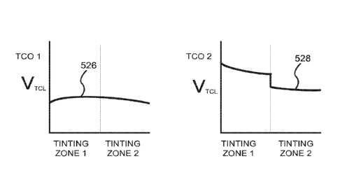
5E includes two graphs showing plots of the local voltage Via in TCO 1 and TCO
2 of the
EC lite, 510, of Figure 5D that drives transition. At the left, a graph shows
a curve 526 of the
local values of Via in the TCO 1. At the right, a graph shows a curve 528 of
the local values
of VTCL in the TCO 2. In this example, when the EC device is energized, the
bottom TCO 1
has a local voltage potential Vrry, across its span similar to that of a
typical transparent
conductor for an EC device. According to curve 526 of Via in TCO 1, the
voltage increases
slightly in the middle away from where bus bars 525(a) and 525(b) are disposed
on TCO 1
where voltage is applied due to the sheet resistance and current passing
through TCO 1. The
increase will be near bus bar 525(a) and bus bar 520 because of the higher
current in this area
due to higher voltage potential between bus bar 525(a) and bus bar 520. But
TCO 2, by
virtue of resistive zone 515, has a higher Tim, in tinting zone 1 than in
tinting zone 2.
According to curve 528 Via in TCO 2, the slight voltage drops between the left
hand side
where bus bar 520 is disposed on TCO 2 and the resistive zone due to sheet
resistance and
current passing through TCO 2. At the resistive zone 515, the voltage sharply
drops. The
voltage slightly drops between the resistive zone 515 and the right hand side
due to sheet
resistance and current passing through TCO 2. The value of Veff at any
location between the
CA 02890749 2015-05-05
WO 2014/078429 PCT/US2013/069913
bus bars is the difference in values of curves 130 and 125 at that position on
the x-axis
corresponding to the location of interest. The result is that tinting zone 1
has a higher Veff
than tinting zone 2 and thus tinting zone 1 colors more darkly than tinting
zone 2. This is
represented in Figure 5F. Of course, the two tinting zones can be configured
as upper and
lower portions when installed in a building, and they need not be side by side
as depicted.
100691 Figure 5G depicts an EC lite, 530, configured with a resistive zone
created by
inhibiting the electrical conductivity of only one of the transparent
conducting oxides. The
EC lite is much like the one described in relation to Figure 5E, but in this
embodiment one of
the TCOs is cut through along the resistive zone (cut 550), while the other
TCO is left intact.
The EC device stack is unchanged in the resistive zone, only the top TCO is
cut. The EC lite
530 has two sets of bus bars, 535 and 540. Bus bar set 535 powers the lower
TCO 1, while
bus bar set 540 powers the top TCO 2. The lower portion of Figure 5G shows
cross section
Z-Z. The EC device will still at least partially color along the resistive
zone by virtue of one
of the TCOs being fully intact, monolithic, along with the EC stack. While
there is a narrow
region of the opposite TCO 2 missing, there is sufficient voltage potential
established
between the intact TCO 1 and the edge of the cut (opposing) TCO 2 along the
resistive zone
to allow coloration of the EC device in the resistive zone, albeit more slowly
than if both
TCOs were intact along the resistive zone. The resistive zone may color more
lightly when
only one of the tinting zones is powered, while with both tinting zones
powered, the resistive
zone may fully tint or approximate full tinting. Each portion of TCO 2 can be
powered
independently of TCO 1. In this way, separate zones, tinting zone 1 and
tinting zone 2, may,
e.g., be tinted more effectively. Since there is a cut through the TCO 2, if
only one zone is
powered, Vra is only established in that tinting zone. The cut in TCO 2 aids
in establishing
and maintaining a uniform tinting front. In this example, since the TCOs are a
type of
moisture barrier, EC lite 530 may be incorporated into an KiU where the EC
device is
hermetically sealed within the volume of the 1GU, and/or a top coat may be
used to
hermetically seal the device, with our without lamination to a substrate. A
top coat would fill
the open trench cut through TCO 2.
[0070] In certain embodiments, it may be more desirable to cut the bottom TCO
I rather than
the top TCO 2. Figure 5H shows EC lite, 530a, where the cut, 550a, is made
only through the
bottom TCO 1. In this example, the top TCO 2 may maintain its hermeticity by
virtue of an
intact top transparent conductor layer. The EC material may fill in the trench
made by cut
21
CA 02890749 2015-05-05
WO 2014/078429 PCT/US2013/069913
550a, and thus tint along with the trench in TCO 1 that it fills, providing an
area of inhibited
coloration rate such as a resistive zone.
[0071] In certain embodiments, it may more desirable to cut the top TCO 2
rather than the
bottom TCO 1. Figure 5G shows EC lite, 530, where the cut, 550, is made only
through the
top TCO 2. An advantage of this embodiment may be that the cut can be made
after the EC
device is fabricated, for example, by laser processing performed after sputter
coating.
[0072] The busbars 535 and 540 depicted in Figures 5G and 5H need not be
parallel, e.g. the
bus bars powering each TCO can be orthogonal to each other. Also, the single
monolithic
TCO need not have two bus bars, but it is desirable so as to have more control
over tinting of
.. the individual tinting zones. Bleaching function would work the same way
but in reverse
polarity to bleach the tinting zones.
[0073] Resistive zones need not be linear as depicted, but rather may be of
any shape. For
example, for desired effects, one might choose a resistive zone that is
zigzagged, curved or
irregularly shaped along adjacent tinting 7ones
[0074] In certain embodiments, resistive zones are used to define a perimeter,
closed or open,
of a region of an EC window. For example, these resistive zones can be used to
highlight
particular symbols or shapes in the viewable region of the EC window. One
embodiment
with such a resistive zone is illustrated in Figures 6A and 6B. For example,
an end user may
wish to have an area of the EC window that does not tint, or that becomes
tinted more slowly,
than the remainder of the Linable EC window.
[0075] Figure 6A depicts an EC lite, 600, which includes a single pair of bus
bars, 105, as
well as a resistive zone, 605. In this example, the resistive zone is in the
shape of a closed
rectangle (as indicated by the dotted line). Resistive zone 605 may not be
visually discernible
to the naked eye. In one embodiment, resistive zone 605 is configured such
that the portions
of the TCOs of the EC device in the resistive zone (as indicated by the dotted
line) have a
higher electrical resistance than the portions of the TCOs in the remainder of
the EC device
on either side of the resistive zone (in this example both outside and inside
the rectangular
perimeter zone), but the resistive zone still passes charge. In this
embodiment, when the EC
device is tinted, the area around the resistive zone 605 tints first, the
tinting front slowing
when it reaches the rectangular closed resistive zone 605. This momentarily,
e.g. for a period
of minutes, gives the effect of a small untinted view port in a larger tinted
window. As the
22
CA 02890749 2015-05-05
WO 2014/078429 PCT/US2013/069913
charge bleeds beyond the resistive zone and into the untinted rectangular
region within the
zone, this gives the effect of the small untinted view port closing as it
tints. In another
embodiment, resistive zone 605 is configured such that the portions of the
TCOs of the EC
device in the resistive zone (as indicated by the dotted line) have a very
high resistance to
electrical charge as compared to the portions of the TCOs in the remainder of
the EC device
on either side of the resistive zone (in this example both outside and inside
the rectangular
perimeter zone), that is, the resistive zone effectively blocks electrical
charge. In this
embodiment, when the area outside the zone is tinted, the area inside the zone
may never tint
because the charge may not be able to pass the resistive barrier 605. This
gives the effect of a
small untintcd view port in a larger tinted window, so long as the EC device
is tinted. In
another embodiment, resistive zone 605 is configured such that the portions of
the TCOs of
the EC device in the resistive zone (as indicated by the dotted line) and in
the region within
the resistive zone have a very high resistance to electrical charge as
compared to the portions
of the TCOs in the remainder of the EC device on the outside of the resistive
zone.
[0076] Figure 6B shows a similar EC lite, 610, having a resistive zone, 615,
which is "open"
by virtue of a gap, 620, in the perimeter. In this example, the resistive zone
615 is configured
to block electrical charge. When the EC device is tinted, the area around the
resistive zone
615 tints first, the tinting front slowing when it reaches the rectangular
closed resistive zone
615, except at the open portion 620, where the tinting front gives the effect
of "pouring in" or
"filling in" (as indicated by the two dotted arrows) the rectangular region
within resistive
zone 615. Eventually, when the area inside resistive zone 615 is tinted,
resistive zone 615
may no longer be discernible to the naked eye, as the EC device colors under
the zone, as
described above. Configuring resistive zones in such a way can be used to
achieve
permanent or transient tinting effects on EC windows, e.g., to display a logo
or words in a
transient manner for presentation during marketing purposes, or to achieve
tinted and non-
tinting zones on an EC lite. EC lites so configured can be incorporated into
1GUs as describe
and/or laminated with mate lites.
[0077] One of ordinary skill in the art, armed with this disclosure, would
appreciate that tint
gradient zones can be used with resistive zones and this combination is within
the scope of
.. the embodiments described herein.
[0078] Although the foregoing embodiments have been described in some detail
to facilitate
understanding, the described embodiments are to be considered illustrative and
not limiting.
23
CA 02890749 2015-05-05
WO 2014/078429
PCT/US2013/069913
It will be apparent to one of ordinary skill in the art that certain changes
and modifications
can be practiced within the scope of the above description and the appended
claims.
24