Note: Descriptions are shown in the official language in which they were submitted.
CA 02891313 2015-05-12
WO 2014/062933 PCT/US2013/065468
TITLE
NETWORK INTERFACE DEVICE AND METHOD
HAVING PASSIVE OPERATION MODE AND NOISE MANAGEMENT
PRIORITY CLAIM
[0001] This application is a non-provisional of, and claims the
benefit and
priority of, U.S. Provisional Patent Application Serial No. 61/714,930, filed
on October
17, 2012.
INCORPORATION BY REFERENCE
[0002] The entire contents of the following applications are hereby
incorporated
by reference: (a) U.S. Provisional Patent Application Serial No. 61/714,930,
filed on
October 17, 2012; (b) U.S. Patent Application Serial No. 13/969,064, filed on
August 16,
2013; (c) U.S. Patent Application Serial No. 13/669,805, filed on November 6,
2012; and
(d) U.S. Provisional Patent Application Serial No. 61/559,598, filed on
November 14,
2011.
CROSS REFERENCE TO RELATED APPLICATIONS
[0003] This application is related to the following commonly-owned, co-pending
patent applications: (a) U.S. Patent Application Serial No. 13/969,064, filed
on August
16, 2013; (b) U.S. Patent Application Serial No. 13/669,805, filed on November
6, 2012;
and (c) U.S. Provisional Patent Application Serial No. 61/559,598, filed on
November
14, 2011.
COPYRIGHT NOTICE
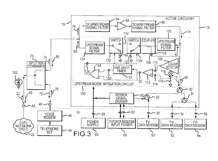
[0004] A portion of the disclosure of this patent document contains
or may
contain material which is subject to copyright protection. The copyright owner
has no
objection to the photocopy reproduction by anyone of the patent document or
the patent
1
CA 02891313 2015-05-12
WO 2014/062933 PCT/US2013/065468
disclosure in exactly the form it appears in the Patent and Trademark Office
patent file
or records, but otherwise reserves all copyrights whatsoever.
BACKGROUND
[0005] Cable television (CATV) networks supply high frequency
"downstream" signals from a main signal distribution facility, known as a
"headend,"
through the CATV network infrastructure, to the homes and offices of
subscribers The
downstream signals are supplied to the subscriber equipment, such as
television sets,
telephone sets and computers, to enable them to operate.
[0006] In addition, most CATV networks also transmit "upstream"
signals
from the subscriber equipment back to the headend of the CATV network. For
example,
a set top box enables the subscriber to select a TV program for display on the
television
set by transmitting the program selection to the CATV provider. Upstream
signals are
sent from the set top box to the headend signal-delivering equipment. This
equipment
responds by transmitting the selected downstream signal to the subscriber. As
another
example, two-way communication occurs when using a personal computer connected
through the CATV infrastructure to the public Internet. As a further example,
voice over
Internet protocol (VOIP) telephone enabled devices use the CATV infrastructure
and the
public Internet as the medium for transmitting two-way telephone
conversations. Such
two-way signal transmission (upstream and downstream) is therefore an
important
feature for modern CATV networks.
[0007] Passive-active network interface devices have been developed
to
provide both passive and active, i.e. amplified, signals at the subscriber
premises for the
two different types of subscriber devices which operate from passive and
active signals.
Such passive-active network interface devices include a signal splitter which
essentially
divides or branches the incoming, or "downstream," signals from the cable
network into
passive and active branches. The passive branch downstream signals are
conducted
through a passive branch of the network interface device without amplification
or
modification and applied to those subscriber devices which require passive
signals for
operation, such as, for example, a voice modem for a telephone set. The active
branch
2
CA 02891313 2015-05-12
WO 2014/062933 PCT/US2013/065468
downstream signals are conducted to an active signal conditioner, such as an
amplifier,
of an active branch of the network interface device. The active signal
conditioner
amplifies the strength of the signals or modifies some characteristic of the
signals
before the amplified, or conditioned, signals are delivered to one or more
subscriber
devices. The amplified signals are applied to those subscriber devices that
benefit from
the amplified signals, such as a television sets and computers.
[0008] The known passive-active interface devices have several
disadvantages. They include electromechanical, moving parts. The moving parts
can
cause higher instances of failure or require undesirable levels of repair and
maintenance. Also, the complexity of the known passive-active interface
devices is
associated with a relatively high manufacturing cost which, in turn, leads to
a higher
price passed along to the users of cable network services.
[0009] The high-frequency signals conducted through the cable
network
are susceptible to distortion from a number of sources. It is for this reason
that coaxial
cables are widely used to shield the high-frequency signals from degrading
influences of
the ambient environment. One requirement for maintaining high-quality signal
conduction in a coaxial cable is properly terminating the coaxial cable. An
improper
termination causes reflections of the incident signals back into the
transmission path.
The reflections cause degradation of the desired incident signals received by
the
subscriber. The degradations are exemplified by amplitude ripple, group delay
ripple,
latency, and other similar effects which distort or reduce the incident
signals. The signal
reflections cause the subscriber to experience a degraded quality of service,
or in some
cases the level of degradation may prevent the subscriber from receiving
meaningful
service.
[0010] Therefore, there is a need to overcome, or otherwise lessen
the
effects of, the disadvantages and shortcomings described above.
3
CA 02891313 2015-05-12
WO 2014/062933 PCT/US2013/065468
SUMMARY
[0011] The network interface device (NID), in one embodiment, is
operable
to connect subscriber equipment to a CATV network over which downstream
signals in
a first frequency band from a headend of the CATV network, are transmitted to
the
subscriber equipment. Valid upstream signals in a second different frequency
band are
transmitted from the subscriber equipment to the headend. The network
interface
device has an upstream noise mitigation circuit which mitigates ingress noise
into the
CATV network in the second frequency band. The network interface device also
has a
bypass circuit for lifeline preservation, including an upstream filter which
filters upstream
signals before delivery to the CATV network, and a bypass circuit is connected
to the
noise mitigation circuit. The bypass circuit includes a lifeline signal path,
and the bypass
circuit includes a relay. The relay switches the signal path between the noise
mitigation
circuit and the lifeline path. The relay switches to the lifeline path during
a power-off
condition.
[0012] In one embodiment, the NID includes a signal splitter that
is
operable to separate a downstream signal into a passive branch signal and/or
an active
branch signal. An active branch circuit transmits the active branch signal to
an active
subscriber device. An active branch circuit noise manager detects an upstream
signal
transmitted from the least one active subscriber device and establishes a
signal path for
the detected upstream signal through the active branch circuit. The NID also
includes a
passive branch circuit to transmit the passive branch signal to a passive
subscriber
device.
[0013] In another embodiment, an NID includes a signal splitter
that
separates a downstream signal into a passive branch signal and/or an active
branch
signal. An active branch circuit transmits the active branch signal to/from an
active
subscriber device. An active branch circuit noise manager detects an upstream
signal
transmitted from the least one active subscriber device and establishes a
signal path for
the detected upstream signal through the active branch circuit. A passive
branch circuit
transmits the passive branch signal to/from passive subscriber device. The NID
also
4
CA 02891313 2015-05-12
WO 2014/062933 PCT/US2013/065468
includes a switch (or bypass relay) operable to control transmission of
signals to/from
the active subscriber device.
[0014] In a further embodiment, an NID includes an input port used
to
communicate with a CATV network. A signal splitter separates a downstream
signal into
a passive branch signal and/or an active branch signal. The NID includes a gas
tube
surge protector located on a connection between the input port and the signal
splitter.
An active branch circuit transmits the active branch signal to/from an active
subscriber
device. An active branch circuit noise manager (or noise mitigation circuit)
detects an
upstream signal transmitted from the least one active subscriber device and
establishes
a signal path for the detected upstream signal through the active branch
circuit. A
passive branch circuit transmits the passive branch signal to/from passive
subscriber
device. A bypass circuit bypasses the signal path through the active branch
circuit
during a power-off condition.
[0015] In another embodiment, a noise mitigation circuit detects an
upstream signal transmitted from an active subscriber device and establishes a
signal
path for the detected upstream signal through the active branch circuit.
[0016] Additional features and advantages of the present disclosure
are
described in, and will be apparent from, the following Brief Description of
the Drawings
and Detailed Description.
CA 02891313 2015-05-12
WO 2014/062933 PCT/US2013/065468
BRIEF DESCRIPTION OF THE DRAWINGS
[0017] Fig. 1 is a perspective view of a network interface device
which
incorporates an embodiment and a block diagram of subscriber equipment shown
connected to a CATV network through the network interface device located at a
subscriber's premises.
[0018] Fig. 2 is a block diagram of portions of a typical CATV
network, with
multiple network interface devices of the type shown in Fig. 1 connected by
drop cables
to cable taps, as well as other aspects of the CATV network.
[0019] Fig. 3 is a block diagram of basic functional components
within the
network interface device shown in Fig. 1.
[0020] Figs. 4, 5 and 6 contain multiple waveform diagrams on a
common
time axis, illustrating the functional features of an upstream noise
mitigation circuit of the
network interface device shown in Fig. 3.
[0021] Fig. 7 is a block diagram of basic functional components of
an
upstream noise mitigation circuit which is an alternative to that shown in
Fig. 3.
[0022] Fig. 8, 9 and 10 contain multiple waveform diagrams on a
common
time axis, illustrating the functional features of the upstream noise
mitigation circuit
shown in Fig. 7.
[0023] Fig. 11 depicts a block diagram of an embodiment of a power
loss
bypass circuit.
[0024] Fig. 12 depicts a circuit layout of the power loss bypass
circuit
shown in Fig. 11.
[0025] Fig. 13 depicts a block diagram of an embodiment of basic
functional components within a network interface device.
[0026] Fig. 14 depicts a block diagram of another embodiment of
basic
functional components within a network interface device.
6
CA 02891313 2015-05-12
WO 2014/062933 PCT/US2013/065468
DETAILED DESCRIPTION
Part I
[0027] The infrastructure of a CATV network may include
interconnected
coaxial cables, signal splitters and combiners, repeating amplifiers, filters,
trunk lines,
cable taps, drop lines and other signal-conducting devices. The CATV network
may be
connected to a subscriber's home via a network interface device. This enables
the
subscriber's devices to communicate with the CATV network.
[0028] An NID or network interface device 10, which incorporates an
embodiment, is shown in Fig. 1. The network interface device 10 includes a
housing 12
which encloses internal electronic circuit components (such as shown in Figs.
3 and 7).
A mounting flange 14 surrounds the housing 12, and holes 16 in the flange 14
allow
attachment of the interface device 10 to a support structure at a subscriber's
premises
18.
[0029] The interface device 10 is connected to a CATV network 20,
which
is shown in a typical topology in Fig. 2. Downstream signals 22 originate from
programming sources at a headend 24 of the CATV network 20, and are conducted
to
the interface device 10 in a sequential path through a main trunk cable 26, a
signal
splitter/combiner 28, secondary trunk cables 30, another signal
splitter/combiner 32,
distribution cable branches 34, cable taps 36, and drop cables 38. Upstream
signals 40
are delivered from the network interface device 10 to the CATV network 20, and
are
conducted to the headend 24 in a reverse sequential path. Interspersed at
appropriate
locations within the topology of the CATV network 20 are conventional repeater
amplifiers 42, which amplify both the downstream signals 22 and the upstream
signals
40. Conventional repeater amplifiers may also be included in the cable taps
36. The
cable taps 36 and signal splitter/combiners 28 and 32 divide a single input
downstream
signal into separate downstream signals, and combine multiple upstream signals
into a
single upstream signal.
[0030] The network interface device 10 receives the downstream
signals
22 from the CATV network 20 at a network connection port 44. The downstream
signals
22 are either passive or active. Passive downstream signals are those signals
which are
7
CA 02891313 2015-05-12
WO 2014/062933 PCT/US2013/065468
conducted through the interface device 10 without amplification, enhancement,
modification or other substantial conditioning. The passive downstream signals
are
delivered from a passive port 45 to passive subscriber equipment, such as a
voice
modem 46 connected to a telephone set 48, or an embedded multimedia network
interface device (EMTA, not shown), located at the subscriber premises 18.
Active
downstream signals are those signals which are amplified, filtered, modified,
enhanced
or otherwise conditioned by power-consuming active electronic circuit
components
within the interface device 10. The conditioned active downstream signals are
divided
into multiple copies and delivered from a plurality of active ports 50, 52, 54
and 56 to
active subscriber equipment located at the subscriber premises 18, such as
television
(TV) sets and/or data modems 58, 60, 62 and 64. Other subscriber equipment,
such as
data processing devices or computers, is connected to the data modems.
[0031] The equipment at the subscriber premises 18 typically
generates
upstream signals 40 (Fig. 2) to the network interface device 10 for delivery
to the CATV
network 20. The upstream signals 40 may be either active or passive upstream
signals
generated by the subscriber equipment connected to the active and passive
ports 45,
50, 52, 54 and 56. For example, one or more of the TV sets 58, 60, 62 and 64
may have
conventional set top boxes (not shown) associated with them to allow the
subscriber/viewer to make programming and viewing selections. Of course, any
computers (not shown) connected to the data modems 58, 60, 62 and 64 typically
communicate upstream signals. The telephone set 48 and the voice modem 46, or
the
EMTA (not shown); also generate upstream signals as a part of their typical
functionality.
[0032] Electrical power for the network interface device 10 is
supplied from
a conventional DC power supply 66 connected to a dedicated power input port
68.
Alternatively, electrical power can be supplied through a conventional power
inserter
(also shown at 58) that is connected to the port 50. The power inserter allows
relatively
low voltage DC power to be conducted through the same port 50 that also
conducts
high-frequency signals. Use of a conventional power inserter connected to one
of the
ports, e.g. port 50, eliminates the need for a separate dedicated power supply
port 68,
8
CA 02891313 2015-05-12
WO 2014/062933 PCT/US2013/065468
or provides an alternative port through which electrical power can also be
applied. The
power supply 66 or the power supplied from the port 50 is typically derived
from a
conventional wall outlet (not shown) within the subscriber premises 18.
[0033] The ports 44, 45, 50, 52, 54, 56 and 68 may be conventional
female coaxial cable connectors which are mechanically connected to the
housing 12
and which are electrically connected to internal components of the interface
device 10.
Coaxial cables from the subscriber equipment and the drop cables 38 (Fig. 2)
are
connected to the interface device 10 by mechanically connecting the
corresponding
mating male coaxial cable connector (not shown) on these coaxial cables to the
female
coaxial cable connectors forming the ports 44, 45, 50, 52, 54, 56 and 68.
[0034] The internal circuit components of one embodiment of the
network
interface device 10 are shown in Fig. 3. Those internal circuit components
include a
conventional bi-directional signal splitter/combiner 70 which separates the
input
downstream signals 22 from the CATV network 20 at the cable port 44 into
passive
downstream signals 72 and active downstream signals 74 within the network
interface
device 10. The passive downstream signals 72 are conducted directly through
the
passive port 45 to the passive subscriber equipment 46 and 48. Passive
upstream
signals 76 created by the passive subscriber equipment 46 and 48 are conducted
through the passive port 45 directly to the signal splitter/combiner 70 to
become
upstream signals 40 in the CATV network 20. The direct signal conductivity
path for the
passive signals in the network interface device 10 avoids subjecting the
passive signals
to potentially adverse influences from electronic components that might fail
or
malfunction, thereby enhancing the reliability of the passive communications
without
increasing the risk of failure. Passive communications are intended to be as
reliable as
possible since they may be used in emergency and critical circumstances.
[0035] The active downstream signals 74 are conducted to active
circuitry
78, where the active downstream signals 74 are amplified, filtered, modified,
enhanced
or otherwise conditioned before delivery through the active ports 50, 52, 54
and 56 to
the subscriber equipment 58, 60, 62 and 64. Active upstream signals 80 are
created by
the subscriber equipment 58, 60, 62 and 64, and also pass through the active
circuitry
9
CA 02891313 2015-05-12
WO 2014/062933 PCT/US2013/065468
78, where those signals are also conditioned or otherwise modified or enhanced
before
being combined at the signal splitter/combiner 70 to become network upstream
signals
40 in the CATV network 20.
[0036] The circuit components of the active circuitry 78 receive
power from
the power supply 66 connected at port 68 or through the power inserter 58
(Fig. 1)
connected at port 50. A power-signal divider 82 separates the high-frequency
active
downstream and upstream signals 74 and 80 at port 50 from the DC power at port
50.
The divider 82 conducts the active signals 74 and 80 from and to high-
frequency signal
conductivity paths within the active circuitry 78, while simultaneously
conducting the DC
power to the active circuitry 78 for use by its electrical power consuming
components.
Electrical power from the dedicated power input port 68 is also conducted to
the power
consuming circuit components of the active circuitry 78.
[0037] The components of the active circuitry 78 which conduct the
downstream active signals 74 include first and second analog downstream
filters 84 and
86 that are connected in series by a linear amplifier 88. The downstream
filters 84 and
86 filter the downstream signals 74 in the downstream 54-1000 MHz frequency
band.
The linear amplifier 88 amplifies, modifies or enhances the downstream signals
74, and
in conjunction with the filters 84 and 86, conditions the downstream signals
74. The
downstream signals 74 are thereafter connected through conventional signal
splitter/combiners 90, 92 and 94 before those downstream signals 74 are
delivered
through the active ports 50, 52, 54 and 56 to the subscriber equipment 58, 60,
62 and
64.
[0038] The active upstream signals 80 created by the subscriber
equipment 58, 60, 62 and 64 are conducted through the active ports 50, 52, 54
and 56
to an upstream noise mitigating circuit 100. The upstream noise mitigation
circuit 100
transfers valid active upstream signals 80 from the subscriber equipment 58,
60, 62 and
64 through the network interface device 10 to the CATV network 20 as upstream
signals
40. These functions are accomplished as described below.
[0039] Valid upstream signals from the subscriber equipment 58, 60,
62
and 64 are conducted through the signal splitter/combiners 92, 94 and 90 to
become
CA 02891313 2015-05-12
WO 2014/062933 PCT/US2013/065468
active upstream signals 80. The upstream signals 80 are applied to a first
upstream
signal bandpass filter 102. Because the downstream signal filter 86 passes
signals only
in the 54-1000 MHz band, valid upstream signals 80 in the frequency band of 5-
42 MHz
are blocked by the downstream signal filter 86 and diverted through the
upstream signal
filter 102. The first upstream signal filter 102 preferably passes signals in
the valid
upstream signal frequency range of 5-42 MHz. Typical ingress noise falls
within most
intensely within the frequency range of 0-15 MHz, so the first upstream filter
102 has the
capability of removing ingress noise at the low frequencies in the range of 0-
5 MHz.
However, ingress noise in the range of 5-15 MHz will be conducted by the
upstream
signal filter 102.
[0040] To mitigate or prevent ingress noise upstream signals from
entering
the CATV network 20 from the network interface device 10, ingress noise
signals
conducted through the first upstream filter 102 are isolated by a first radio
frequency
(RF) single pole double throw (SPDT) electronic switch 104 and terminated to
ground
through a termination resistor 103. The termination resistor 103 is connected
to one
terminal of the first electronic switch 104. Signals from the first upstream
signal filter 102
are conducted through a conventional directional coupler 105 to and through
the switch
104 to the termination resistor 103 while the first electronic switch 104 is
in a normal
position, shown in Fig. 3. All signals conducted through the first upstream
signal filter
102 are terminated through the termination resistor 103, and are thereby
prevented
from entering the CATV network 20, while the first switch 104 is in its normal
position.
[0041] The first electronic switch 104 changes to an alternate
activated
position (not shown in Fig. 3) upon the instantaneous power of the signals
conducted
through the filter 102 reaching a magnitude indicative of a valid upstream
signal from
the subscriber equipment 58, 60, 62 or 64. To distinguish relatively low power
ingress
noise from the relatively higher power of a valid upstream signal, the
instantaneous
magnitude of the power of the signals passing through the upstream filter 102
is
detected and evaluated. The coupler 105 delivers a signal 106 which is
typically 10dB
lower in power than the signal passing through the coupler 105 to the switch
104.
11
CA 02891313 2015-05-12
WO 2014/062933 PCT/US2013/065468
[0042] The signal 106 from the coupler 105 is conducted to an input terminal
of a
conventional log amplifier detector 108. The log amplifier detector 108
operates on an
inverse logarithmic basis to convert the instantaneous magnitude of power of
the signal
106 to a DC voltage output signal 110. By operating on an inverse logarithmic
basis, the
typical decibel power of the input signal 106 is converted into a linear DC
voltage output
signal 110 whose magnitude is inversely related to the instantaneous input
power. This
logarithmic conversion allows the log amplifier detector 108 to function as an
instantaneous demodulating power detector whose output DC voltage signal is
inversely
proportional to the logarithm of the input power. In one embodiment, the log
amp
detector 108 includes a commercially available component identified as part
number AD
8319 available from Analog Devices of Norwood Massachusetts, USA. The DC
voltage
output signal 110 therefore represents the inverse of the instantaneous power
of the
upstream signal 80 conducted through the directional coupler 105.
[0043] The DC voltage output signal 110 from the log amp detector
108 is
applied to a negative input terminal of a comparator 112. A threshold signal
114 is
applied to the positive input terminal of the comparator 112. The threshold
signal 114 is
derived from a resistor divider network such as a potentiometer 116 and a
resistor 118
connected in series, or from another voltage source. Adjustment of the value
of the
potentiometer 116 adjusts the magnitude of the threshold signal 114. The
adjustment of
the threshold signal 114 establishes the level where a trigger signal 120 from
the
comparator 112 switches from a logic low level to a logic high level.
[0044] The magnitude of the DC voltage output signal 110 from the
log
amp detector 108 is inversely related to the magnitude of the instantaneous
power of
the upstream signal represented by signal 106. That is, when the magnitude of
the
upstream signal 106 is relatively large, the DC voltage output signal 110 from
the log
amp detector 108 is relatively small, and vice versa. Because of this inverse
relationship, the DC voltage output signal 110 is applied to the negative
input terminal of
the comparator 112, and the threshold signal 114 is applied to the positive
input
terminal of the comparator 112. Applying the two input signals in this manner
causes
the comparator 112 to supply a logic high trigger signal 120 whenever the
magnitude of
12
CA 02891313 2015-05-12
WO 2014/062933 PCT/US2013/065468
the instantaneous power of the upstream signal exceeds a predetermined
threshold
power level representative of a valid upstream signal. Conversely, when the DC
voltage
output signal 110 is greater than the signal 114, the trigger signal 120 from
the
comparator 112 is at a logic low level. When the DC voltage output signal 110
is less
than the signal 114, the trigger signal 120 from the comparator is at a logic
high level.
The logic high level of the signal 120 therefore represents the condition
where the
instantaneous power of the upstream signal exceeds the predetermined threshold
power level established by the signal 114.
[0045] Upon sensing that the instantaneous power content of an
upstream
signal exceeds the level represented by the predetermined threshold power
level, the
upstream signal is automatically or immediately transmitted or passed to the
CATV
network 20 as a network upstream signal 40. Upstream signals which do not meet
the
threshold power level are considered ingress noise. Ingress noise signals are
isolated
from the CATV network 20 by the switches 104 and 130, while incident upstream
signals 80 are simultaneously terminated to ground through the termination
resistor 103.
The functions of passing upstream signals to the CATV network and terminating
upstream signals to ground are accomplished in response to the logic level of
the trigger
signal 120 from the comparator 112.
[0046] When instantaneous power content of an upstream signal
exceeds
the threshold power level, the resulting logic high signal 120 from the
comparator 112
triggers a one-shot timer 122. Simultaneously, the logic high signal 120 is
applied to an
input terminal of an OR gate 124. The OR gate 124 responds by applying a logic
high
control signal 126 to the control terminals of the first SPDT RF electronic
switch 104 and
a second SPDT RF electronic switch 130. The electronic switches 104 and 130
normally occupy the positions shown in Fig. 3. Upon the assertion of logic
high control
signal 126, the switches 104 and 130 immediately change from their normal
positions
(shown in Fig. 3) to their opposite activated positions (not shown). The
activated
positions of the switches 104 and 130 establish a direct connection over
conductor 132
between the switches 104 and 130. Since the electronic switches 104 and 130
switch
13
CA 02891313 2015-05-12
WO 2014/062933 PCT/US2013/065468
with radio frequency speed, the switches 104 and 130 assume the activated
position
almost instantaneously in response to the assertion of the control signal 126.
[0047] The activated positions of the switches 104 and 130 conduct
the
upstream signal 80 from the first upstream signal filter 102 through the
conductor 132 to
a second upstream signal filter 134. Both filters 102 and 134 suppress
frequencies other
than those in the frequency band of 5-42 MHz. The valid upstream signal flows
from the
second upstream filter 134 through the signal splitter/combiner 70 into the
cable
network 20 as the network upstream signal 40. Terminating resistors 103 and
190 are
connected to the filters 102 and 134 when the switches 104 and 130 are in
their normal
positions, and the filters 102 and 134 are connected together over the
conductor 132
when the switches 104 and 130 are in their activated positions.
[0048] Valid upstream signals are conducted to the CATV network
almost
instantaneously when the instantaneous power level of the upstream signals
exceeds
the threshold power level. By responding almost instantaneously when the
threshold
power level is exceeded, the chances are minimized that the information
contained in
the valid upstream signal will be lost, as might be the case if the power of
the upstream
signal had to be integrated over a time period before a determination of a
valid
upstream signal could be made on the basis of energy content. Such integration
raises
the possibility that some of the information of the upstream signal will be
lost and not
transferred upstream. In contrast, no integration of the power of the upstream
signal
over a selected time period is required in the upstream noise mitigation
circuit 100. By
almost instantaneously transmitting upstream signals which have a power
content that
exceeds the predetermined threshold power level, the integrity of the
information
contained in the upstream signal is better preserved.
[0049] Once the switches 104 and 130 have been moved to the
activated
position which directly connects the first and second upstream signal filters
102 and 134
through the conductor 132, the switches 104 and 130 are maintained in this
activated
position for a time determined by the one-shot timer 122. When triggered by
the logic
high signal 120, the one-shot timer 122 immediately supplies a logic high
output signal
136 to the OR gate 124. Either logic high signal 120 or 136 causes the OR gate
124 to
14
CA 02891313 2015-05-12
WO 2014/062933 PCT/US2013/065468
supply the logic high control signal 126. If the power level of the upstream
signal falls
below the level of the threshold signal 114, the signal 120 immediately
assumes a logic
low level. However, the one-shot timer 122 will continue to deliver the logic
high output
signal 136 for the time duration of its internal time constant.
[0050] The internal time constant of the one-shot timer 122 is
equal to the
amount of time to transmit a single valid upstream signal packet of the
maximum time
duration permitted by the signaling protocol, plus a slight additional amount
of time to
account for inherent tolerances in the components and the timing of the one-
shot timer
122. In this manner, the one-shot timer 122 ensures that the switches 104 and
130
assume their activated positions for a long enough time to conduct all single
valid
upstream signals, including a maximum-length valid upstream signal or packet.
[0051] The situation just described is illustrated by the waveform
diagrams
shown in Fig. 4, taken in connection with Fig. 3. The signal 106 represents a
single valid
upstream packet of the permitted maximum time duration whose detection by the
log
amp detector 108 produces the logic high trigger signal 120. The signal 120
assumes
the logic high level at time point 138, triggering the one-shot timer 122 and
causing the
output signal 136 to be asserted at the same time point 138. The control
signal 126 from
the OR gate 124 immediately assumes a logic high level at time point 138. The
electronic switches 104 and 130 assume their activated positions for the
duration of the
logic high control signal 126. At time point 139, the maximum time duration of
a single
valid upstream packet or signal ends, and the instantaneous power represented
by that
signal falls below the threshold power level represented by the threshold
signal 114.
The signal 120 assumes a logic low level. Since the time constant of one-shot
timer 122
is established to slightly exceed the maximum time duration of a single valid
upstream
packet or signal, the logic high signal 136 will continue to time point 140.
When the
signal 136 assumes a logic low level after the one-shot timer 122 times out at
time point
140, the control signal 126 from the OR gate 124 simultaneously assumes a
logic low
level. As a result, the control signal 126 is longer in duration than signal
120. When the
control signal 126 assumes the low logic level at time point 140, the
electronic switches
104 and 130 assume their normal positions to conduct any upstream signals to
the
CA 02891313 2015-05-12
WO 2014/062933 PCT/US2013/065468
termination resistor 103, thereby terminating those signals to ground and
preventing the
further upstream signals from reaching the CATV network.
[0052] For multiple valid upstream signal packets which are
consecutively
transmitted without a substantial time interval separating the multiple
sequential
upstream packets, the one-shot timer 122 will time out before the valid
upstream signal
transmission terminates. However, the continuous instantaneous power of the
multiple
sequential valid upstream signal packets will continue to exceed the threshold
power
level for the duration of the multiple sequential signal packets, thereby
causing the
comparator 112 to continue to assert the logic high trigger signal 120 to the
OR gate
124 for the duration of the multiple sequential signal packets. The continued
application
of the logic high signal 120 causes the OR gate 124 to assert the logic high
control
signal 126 beyond the time when the one-shot timer 122 times out. The two
upstream
signal filters 102 and 134 remain connected by the switches 104 and 130 in
their
activated positions, and thereby conduct the multiple sequential upstream
signal
packets to assure that the full information represented by the multiple
sequential signal
packets is not truncated or lost by premature termination of those signals. At
the
termination of such multiple upstream signal packets, the signal power no
longer
exceeds the threshold signal 114, and the switches 104 and 130 immediately
assume
their normal positions, thereby preventing any ingress noise from entering the
CATV
network 20 after the longer or multiple sequential valid upstream packets have
been
transmitted.
[0053] The situation just described is illustrated by the waveform
diagrams
shown in Fig. 5, taken in conjunction with Fig. 3. The signal 106 represents
three, for
example, sequential valid upstream packets or signals. The trigger signal 120
assumes
the logic high level at time point 142 in response to recognizing the first of
the
sequential valid upstream packets. The one-shot timer 122 is triggered and
causes the
output signal 136 to be asserted at time point 142. The control signal 126
from the OR
gate 124 also assumes a logic high level at time point 142 in response to the
assertion
of the control signal 136. The electronic switches 104 and 130 assume their
activated
positions in response to the logic high control signal 126. At time point 140,
the one-shot
16
CA 02891313 2015-05-12
WO 2014/062933 PCT/US2013/065468
timer 122 times out, causing its output signal 136 to assume a logic low
level. However,
the instantaneous power level from the multiple sequential upstream signal
packets
continues to exceed the threshold power level, until the sequence of multiple
upstream
signal packets terminates at time point 146. So long as the signal 120 is at a
logic high
level, the control signal 126 from the OR gate 124 causes the electronic
switches 104
and 130 to remain in the activated position, conducting the multiple
sequential valid
upstream signal packets to the CATV network 20. Once the sequence of multiple
valid
upstream signal packets has been transmitted, which occurs at time point 146,
the
absence of any further valid upstream signal causes the instantaneous power
level to
fall below the threshold power level, and the signals 120 and 126 assume a
logic low
level. The electronic switches 104 and 130 respond by assuming their normal
positions
to prevent the further transmission of upstream signals to the CATV network.
[0054] If the instantaneous power of ingress noise exceeds the
threshold
power level, the electronic switches 104 and 130 assume their activated
positions, as
can be understood from Fig. 3. An unusually high and short duration power
level of
ingress noise can cause this situation. Under that circumstance, the trigger
signal 120
assumes a logic high level, and the one-shot timer 136 is triggered and
asserts the
output signal 136. The electronic switches 104 and 130 assume their activated
positions, allowing the ingress noise to pass through the upstream filters 102
and 134.
Until the one-shot timer 122 times out, ingress noise will be allowed to enter
the CATV
network 20. The effect of this ingress noise is minimized by the time constant
of the
one-shot timer 122 extending only for the maximum time duration of the longest
single
valid upstream signal packet permitted under the communication protocol.
[0055] The response to ingress noise having instantaneous power
that
exceeds the threshold is illustrated by the waveform diagrams shown in Fig. 6,
taken in
connection with Fig. 3. The ingress noise signal is shown at 106. Because the
instantaneous power of the ingress noise exceeds the threshold, a logic high
trigger
signal 120 is asserted from the comparator 112 at time point 148, thereby
triggering the
one-shot timer 122 and causing the signal 136 to be asserted at the same time
point
148. The logic high signal 136 causes the OR gate 124 to assert the logic high
control
17
CA 02891313 2015-05-12
WO 2014/062933 PCT/US2013/065468
signal 126 at time point 148. The electronic switches 104 and 130 assume their
activated positions for the duration of the high level of the control signal
126. At time
point 150, the instantaneous power from the ingress noise falls below the
threshold
power level, causing the comparator 112 to assert a logic low trigger signal
120.
However, the one-shot timer 122 has not timed out and continues to deliver the
logic
high signal 136 for the time duration of its time constant, until time point
140. The
control signal 126 from the OR gate 124 transitions to a logic low level at
time point 140
when the one-shot timer 122 times out, causing the electronic switches 104 and
130
(Fig. 3) to assume their normal positions. The electronic switch 104 connects
the
termination resistor 103 to terminate any further upstream signals to ground
and thereby
prevent any further transfer of upstream signals to the CATV network.
[0056] An alternative form 160 of the upstream noise mitigation
circuit,
shown in Fig. 7, reduces the amount of time that ingress noise may be
conducted to the
CATV network 20 after the initial instantaneous power of the ingress noise is
sufficient
to exceed the threshold power level, compared to the response of the circuit
100 (Fig.
3). The upstream noise mitigation circuit 160 shown in Fig. 7 includes many of
the same
components as the upstream noise mitigation circuit 100 (Fig. 3), and those
same
components function in the manner previously described.
[0057] In response to the instantaneous power of the ingress noise
exceeding the threshold power level, represented by signal 114, the comparator
112
supplies the logic high trigger signal 120, in the manner previously
described. The logic
high trigger signal 120 is applied to a one-shot timer 162, to the input
terminal of a
SPDT RF electronic switch 164, to a second one-shot timer 168, and to the set
terminal
of a set-reset latch 172. In response to the logic high signal 120, the first
one-shot timer
162 triggers and supplies an output signal 166. Simultaneously, the second one-
shot
timer 168 is triggered and supplies a signal 170. The latch 172 is immediately
set in
response to the logic high trigger signal 120 and supplies the control signal
126 to the
RF electronic switches 104 and 130, causing them to switch to their activated
positions
and establish the upstream signal communication path for conducting upstream
signals
through the upstream signal filters 102 and 134. In this manner, the noise
mitigation
18
CA 02891313 2015-05-12
WO 2014/062933 PCT/US2013/065468
circuit 160 responds almost instantaneously to the instantaneous power of the
upstream
signal exceeding the threshold to immediately conduct the upstream signal to
the CATV
network without delay and without the risk of diminishing or losing some of
the
information contained in the upstream signal. In this regard, the upstream
noise
mitigation circuit 160 (Fig. 7) is similar in initial response to the upstream
noise
mitigation circuit 100 (Fig. 3). However, the upstream noise mitigation
circuit 160 has
the capability of more quickly closing the upstream communication path through
the
switches 104 and 130 when the upstream communication path was initially
established
in response to ingress noise.
[0058] The rapid closure of the upstream communication path in
response
to ingress noise is accomplished by integrating the signal 120 for a
predetermined time
established by the time constant of the one-shot timer 162. The logic high
trigger signal
120 represents the power of the ingress noise exceeding the predetermined
threshold
power level. Integrating the logic high trigger signal 120 results in a value
which
represents energy above the threshold power level for the time duration of
integration.
Integration occurs over the time that the signal 166 is asserted by the one-
shot timer
162. If the amount of power integrated during this time, i.e. energy, is not
sufficient to
confirm a valid upstream signal with continuous sustained instantaneous power,
the
switches 104 and 130 are moved to their normal positions, thereby terminating
the
upstream communication path. Since ingress noise generally does not contain
significant sustained energy even though an initial burst of the ingress noise
may have
sufficient instantaneous power to exceed the threshold, the upstream
communication
path is quickly closed in a typical ingress noise situation.
[0059] Integrating the power represented by the threshold power
level is
accomplished by an integration circuit 179. The integration circuit 179
includes an
operational amplifier 176. The positive input terminal of the operational
amplifier 176 is
connected to ground reference. A capacitor 178 is connected between the
negative
input terminal and the output terminal of the operational amplifier 176. The
negative
input terminal of the operational amplifier 176 is the input point for signals
to the
integration circuit 179.
19
CA 02891313 2015-05-12
WO 2014/062933 PCT/US2013/065468
[0060] Prior to commencement of integration, the switch 164 is in
its
normal position shown in Fig. 7. In the normal position of the switch 164, a
positive
voltage signal 171 is conducted from a power supply source 175 to a resistor
174 which
is connected to the negative input terminal of an operational amplifier 176.
Applying the
positive voltage to the negative input terminal of the operational amplifier
176 has the
effect of causing integration across the capacitor 178 to establish an output
signal 180
at a voltage level near the ground reference. A voltage level near the ground
reference
constitutes a logic low signal. Thus, in the normal position of the switch
164, the output
signal 180 from the integrator circuit 179 is at a logic low level.
[0061] In response to the control signal 166 moving the switch 164
from its
normal position shown in Fig. 7 to its activated position which is the
alternate of that
position shown in Fig. 7, the logic high trigger signal 120 is applied through
the resistor
174 to the negative input terminal of the operational amplifier 176. So long
as the trigger
signal 120 is at the logic high level, the output signal 180 from the
operational amplifier
176 remains at a logic low level. However, because ingress noise typically has
the
effect of rapidly subsiding in instantaneous power, the instantaneous power
will usually
not exceed the threshold for a significant sustained amount of time, thereby
causing the
signal 120 to assume a logic low level during the time that the one-shot timer
162
supplies the control signal 166. Consequently, with the switch 164 in the
activated
position and the signal 120 at a logic low level, the operational amplifier
176 integrates
this change of input signal level across the capacitor 178, which causes the
output
signal 180 to start increasing from the ground reference level. If the
instantaneous
power of the ingress noise remains low for a significant portion of the time
that the one-
shot timer 162 asserts the control signal 166, as is typical with ingress
noise having an
initial momentarily-high instantaneous power burst, the voltage across the
capacitor 178
will increase to a level which corresponds to a logic high level of the signal
180.
[0062] The logic high output signal 180 is applied to one input
terminal of
an AND gate 167. The control signal 166 is applied to another input terminal
of the AND
gate 167. The input terminal to which the control signal 166 is applied is an
inverting
input terminal, thereby causing the AND gate 167 to respond to the inverted
logic level
CA 02891313 2015-05-12
WO 2014/062933 PCT/US2013/065468
of the control signal 166. The signal 180 remains at a logic high level for a
time period
after integration ceases from the integration circuit 179, and the control
signal 166
assumes the logic low level at the end of the integration time established by
the one-
shot timer 162. At that point, the AND gate 167 responds to two logic high
signals (the
logic low signal 166 is inverted at the input terminal), resulting in a logic
high level signal
169 applied to an OR gate 182. The OR gate 182 supplies a logic high level
signal 184
to a reset terminal of the latch 176. The latch 176 resets, and de-asserts the
control
signal 126 to the switches 104 and 130, thereby closing the upstream
communication
path through the upstream filters 102 and 134. Thus, soon after the initial
instantaneous
power of the ingress signal diminishes and the integration time set by the one-
shot timer
162 expires, the upstream communication path is closed to the further
conduction of
upstream signals, thereby preventing any further ingress noise from entering
the CATV
network.
[0063] During the time and situation just described, another AND
gate 185
has no effect on the functionality. The signal 170 supplied by the one-shot
timer 168 is
asserted for a considerably longer period of time than the one-shot timer 162
asserts
the control signal 166. The time of assertion of the signal 170 is the length
of time, plus
a margin for component tolerances, of the longest single valid upstream packet
or signal
permitted under the signal communication protocol. The time of integration
represented
by the assertion of the control signal 166 is considerably less than the
longest single
valid upstream packet. During the integration of the instantaneous power of
the ingress
noise over the time duration of the control signal 166, the output signal 170
is at a logic
high level, the control signal 126 is at a logic high level because the latch
172 will have
been set by the trigger signal 120, before the signal 120 assumes a logic low
level after
the initial high instantaneous power of the ingress noise has dissipated. The
input
terminals of the AND gate 185 to which the signals 120 and 170 are applied are
inverting. Thus, under these conditions, the AND gate 185 supplies an output
signal 187
at a logic low level.
[0064] The situation of terminating the upstream communication path
created by a burst of ingress noise before expiration of the time duration of
a maximum-
21
CA 02891313 2015-05-12
WO 2014/062933 PCT/US2013/065468
length valid upstream signal or packet is illustrated by the waveform diagrams
shown in
Fig. 8, taken in connection with Fig. 7. The ingress noise signal is shown at
106. The
instantaneous power of the ingress noise exceeds the threshold power level and
causes
a logic high trigger signal 120 from the comparator 112 at time point 148,
thereby
triggering the one-shot timers 162 and 168 and causing the control signals 166
and 170
to be asserted at the time point 148. The control signal 126 from the latch
172 also
assumes a logic high level at time point 148 because the logic high trigger
signal 120
sets the latch 172. The electronic switches 104 and 130 assume their activated
positions for the duration of the logic high control signal 126 to maintain
the upstream
communication path. At time point 150, the instantaneous power of the ingress
noise
falls below the threshold power level, and the trigger signal 120 assumes a
logic low
level. However, the first one-shot timer 162 has not timed out and continues
to deliver
the control signal 166 until it times out at time point 188. The time duration
between time
points 148 and 188 is the time constant of the one-shot timer 162 which
establishes the
time duration of integration. The time for integrating a valid upstream signal
is the time
between time points 148 and 188.
[0065] If the integrated value indicates an upstream signal of
unsustained
instantaneous power, consistent with ingress noise that rapidly dissipates,
the resulting
logic high signal 180 from the integrator 179 is applied to the OR gate 182.
The OR gate
182 supplies the logic high signal 180 at time point 188 which, when logically
AND-ed
with the logical inversion of signal 166, causes the AND gate 167 to assert
the signal
169. The OR gate 182 responds by asserting a logic high signal 184, which
resets the
latch 172, thereby de-asserting the control signal 126. The upstream
communication
path is terminated when the switches 104 and 130 assume their normal
positions.
[0066] As is understood from Fig. 8, the upstream communication
path
remains open from time point 148 to time point 188. This time is considerably
less than
the maximum time length of a single valid upstream packet or signal,
represented by the
time between points 148 and 189, or between time points 148 and 150 (Fig. 6).
Consequently, even though the upstream communication path is immediately
established to allow upstream signal communication whenever the instantaneous
power
22
CA 02891313 2015-05-12
WO 2014/062933 PCT/US2013/065468
exceeds the threshold, that upstream communication path is closed to further
upstream
communication very rapidly thereafter if spurious ingress noise established
that
communication path.
[0067] Whenever an upstream signal has sustained instantaneous
power,
the noise mitigation circuit 160 assures that the upstream signal will be
conducted to the
CATV network. Such circumstances indicate a valid upstream signal. As
understood
from Fig. 7, the trigger signal 120 is asserted at a logic high level when the
valid
upstream signal exceeds the threshold. The latch 172 is set and asserts the
logic high
control signal 126 which moves the switches 104 and 132 their activated
positions to
establish the upstream communication path. The timers 162 and 168 are
triggered, and
the one-shot timer 162 moves the switch 164 to its activated position. The
output signal
180 remains at a logic low level during the time of a valid upstream signal
while the one-
shot timer 162 asserts the control signal 166 and while the logic high trigger
signal 120
remains at a logic high level due to the sustained instantaneous power of the
valid
upstream signal exceeding the threshold. The logic low signal 180 and the
inversion of
the logic high signal 166 at the input terminal of the AND gate 167 causes the
AND gate
167 to assert a logic low signal 169, which has no effect on the OR gate 182
or the latch
172. Thus, during the transmission of a valid upstream signal, the AND gate
167 has no
effect on the status of the latch 172.
[0068] On the other hand, the time constant of the one-shot timer
168 is
considerably longer than the time constant of the one-shot timer 162. The
signal 170
from the timer 168 is asserted for the time duration of a single valid maximum-
length
upstream packet or signal. The logic high level of the signal 170 is inverted
at the input
terminal of the AND gate 185. At this time, the control signal 126 is at a
logic high level
because the latch 172 has been set. The continuous instantaneous power of the
valid
upstream signal is represented by a logic high level of the trigger signal
120. The logic
high level of the signal 120 is inverted at the AND gate 185. The logic level
of the
signals applied to the AND gate 185 causes it to supply a logic low signal
187, which
has no effect on the latch 172 during conditions of sustained instantaneous
power from
the valid upstream signal.
23
CA 02891313 2015-05-12
WO 2014/062933 PCT/US2013/065468
[0069] When the valid upstream signal terminates, the logic high
level of
the signal 120 changes to a logic low level. The logic low level signal 120 is
inverted at
its input terminal to the AND gate 185. The logic high signal 170 is still
asserted by the
one-shot timer 168, because the timer 168 times the duration of a single valid
maximum-length upstream signal. Until the one-shot timer 168 de-asserts the
signal
170, the AND gate 185 will not assert a logic high signal 187. However, when
the signal
170 is de-asserted, the AND gate 185 applies the logic high signal 187 to the
OR gate
182. The OR gate 182 asserts the signal 184 to reset the latch 172, and the
control
signal 126 is de-asserted. The switches 104 and 132 move to their normal
positions and
terminate the upstream communication path through the filters 102 and 134.
[0070] In response to sustained instantaneous power representative
of a
valid upstream signal, the noise mitigation circuit 160 assures that an
upstream
communication path will be established for the maximum time duration of a
single valid
upstream signal, provided that there is sufficient instantaneous energy in the
upstream
signal during the integration time established by the signal 166. In this
manner, the
circuit 160 is similar to the circuit 100 (Fig. 3) which assures that the
upstream
communication path remains established for the time duration of a single valid
maximum-length upstream signal or packet. However, unlike the circuit 100
(Fig. 3) the
circuit 160 discriminates between short-duration high instantaneous power
ingress
noise and continuous-duration high instantaneous power upstream signals and
rapidly
terminates the upstream communication path in response to the former.
[0071] The situation of maintaining the upstream communication path
in
response to sustained instantaneous energy of an upstream signal during the
integration time established by the time constant of the one-shot timer 162,
to allow
adequate time for a single valid upstream packet of maximum duration to be
transmitted, is illustrated by the waveform diagrams shown in Fig. 9, taken in
connection
with Fig. 7. The upstream signal is represented by a packet having a time
duration less
than the maximum allowed time duration for single valid upstream packet as
shown at
106. The instantaneous power of the upstream packet 106 exceeds the threshold
power
level and causes a logic high trigger signal 120 from the comparator 112 at
time point
24
CA 02891313 2015-05-12
WO 2014/062933 PCT/US2013/065468
148, thereby triggering the one-shot timers 162 and 168 and causing the
control signals
166 and 170 to be asserted at the same time point 148. The control signal 126
from the
latch 172 also assumes a logic high level at time point 148 due to the
assertion of the
logic high signal 120. The electronic switches 104 and 130 assume their
activated
positions for the duration of the logic high signal 126 and establish the
upstream
communication path. At time point 188, the first one-shot timer 162 times out
and de-
asserts the control signal 166. The time duration between time points 148 and
188
establishes the time duration of integration.
[0072] During the time of integration, the instantaneous power of
the single
packet 106 continuously exceeds the threshold level. Consequently, the output
signal
180 from the integration circuit 179 remains at a logic low level, and the
inversion of the
control signal 166 at the AND gate 167 maintains the output signal 169 in a
logic low
level. At time point 188 when the one-shot timer 162 times out, the control
signal 166
assumes a logic low level, but the inversion of that logic low level at the
input terminal to
the AND gate 167, coupled with the continuous logic low level signal 180
continues to
maintain the output signal 169 at a logic low level. The logic low signal 169
does not
change for the duration of the situation shown in Fig. 9. As a result, the AND
gate 167
has no effect on resetting the latch 172 in this situation.
[0073] During the time between points 148 and 188, the logic high
control
signal 126, the logic high trigger signal 120, which is inverted at its input
terminal to the
AND gate 185, and the logic high control signal 170, which is also inverted at
its input
terminal to the AND gate 185, cause the output signal 187 from the AND gate
185 to
remain at a logic low level. Therefore, during this time between points 148
and 188, the
signal 187 from the AND gate 185 has no effect on resetting the latch 172.
[0074] At time point 190 the packet 106 terminates. The
instantaneous
power associated with the packet 106 also terminates, causing the trigger
signal 120 to
achieve a logic low level. However, the one-shot timer 168 has not yet timed
out, so its
output signal 170 remains at a logic high level until time point 189. The
logic low level
trigger signal 120 does not change the state of the AND gate 185.
Consequently, the
latch with 172 remains set at time point 190.
CA 02891313 2015-05-12
WO 2014/062933 PCT/US2013/065468
[0075] When the one-shot timer 168 times out, at point 189, the
control
signal 170 assumes a low logic level. The low logic signal 170 is inverted at
its input
terminal to the AND gate 185. The trigger signal 120 previously assumed a
logic low
level at time point 190. The inversion of the signals 120 and 170 at the input
terminals to
the AND gate 185 results in three logic high input signals to the AND gate
185, causing
the output signal 187 to assume a logic high level. The logic high signal 187
is applied
to the OR gate 182, and the output signal 184 from the OR gate resets the
latch 172.
Upon reset, the latch 172 de-asserts the control signal 126 at time point 189,
thereby
closing the upstream communication path through the filters 102 and 134 as a
result of
the switches 104 and 130 assuming their normal positions.
[0076] Thus, as is understood from Fig. 9, a valid upstream signal
of any
duration will exceed the minimum power threshold measured during the
integration time
established by the one-shot timer 162, and as a consequence, the latch 172
will
continue to assert the control signal 126 and maintain the upstream
communication
path through the filters 102 and 104. The upstream communication path will be
maintained for the duration of the time constant of the one-shot timer 168,
during which
its output signal 170 is asserted at a logic high level. By maintaining the
upstream
communication path during the time that the one-shot timer 168 asserts the
control
signal 170, it is assured that all valid upstream signals having a time length
at least
equal to the maximum length of a single valid upstream signal will pass
through the
upstream communication path. Consequently, none of the information contained
in a
single valid upstream packet will be lost or truncated.
[0077] The upstream signal communication path remains established
during the time between the actual end of the valid upstream packet and the
end of a
maximum-length valid upstream packet, represented by the difference in time
between
points 190 and 189, but that amount of time is relatively short and
maintenance of the
upstream communication path during this time assures that a valid upstream
signal
packet of any length up to the maximum length will be transmitted without loss
or
truncation of any of its information.
26
CA 02891313 2015-05-12
WO 2014/062933 PCT/US2013/065468
[0078] In addition to the previously described advantages of
quickly
closing the upstream communication path after it was established by ingress
noise and
of establishing the upstream communication path for the maximum length of a
valid
upstream signal, the noise mitigation circuit 160 also has the capability of
transmitting
multiple sequential valid data packets, without loss or truncation of
information. This
situation can be understood by reference to Fig. 10, taken in conjunction with
Fig. 7.
[0079] The first valid upstream packet of the sequence of multiple
valid
upstream packets, shown at 106 in Fig. 10, establishes the upstream
communication
path due to its sustained instantaneous energy. This energy is sustained
during the
integration time established by the one-shot timer 162. The control signal 166
is
asserted at a high logic level until time point 188, and the control signal
170 is asserted
at a high logic level until time point 189.
[0080] The instantaneous power of the sequence of multiple valid
upstream packets remains above the threshold level and the trigger signal 120
remains
asserted at a logic high level for the duration of that sequence of packets
until time point
193, when the instantaneous power of the multiple sequential upstream packets
terminates. The one-shot timer 168 does not time out until time point 189, at
which point
its output signal 170 assumes a logic low level at time point 189. The low
logic level of
the control signal 170 is inverted at its input terminal to the AND gate 185.
However, at
time point 189, the states of the input signals to the AND gate 185 result in
the AND
gate 185 supplying a logic low output signal 187. The logic low output signal
187 has no
effect on the OR gate 182 and the latch 172 remains set.
[0081] At time point 193, the instantaneous power of the sequence
of
multiple valid upstream packets 106 falls below the threshold, causing the
trigger signal
120 to assume a logic low level. The logic low level of the signal 120 at time
point 193 is
inverted at its input terminal to the AND gate 185, causing the AND gate to
assert a
logic high output signal 187. The logic high signal 187 causes the OR gate 182
to assert
the signal 184, thereby resetting the latch 172 and de-asserting the signal
126. The
switches 104 and 130 assume their normal positions, thereby terminating the
communication path through the upstream signal filters 102 and 134.
27
CA 02891313 2015-05-12
WO 2014/062933 PCT/US2013/065468
[0082] In this manner, the upstream communication path is
maintained for
the duration of the multiple sequential packets, represented by the time
between points
148 and 193. However, after the last packet in the multiple sequential series
of valid
upstream packets ends, the upstream communication path is closed to the
further
transmission of upstream signals, thereby preventing ingress noise from
entering the
CATV network.
[0083] As has been described in conjunction with Figs. 7-10, any
upstream
signal, whether a valid upstream signal or ingress noise, which has sufficient
instantaneous power to exceed the threshold will immediately open the upstream
communication path through the filters 102 and 134. In this sense, the noise
mitigation
circuit 160 does not distinguish between a valid upstream signals and invalid
ingress
noise which may have sufficient energy to exceed the threshold. Not
distinguishing
between these signals assures that there is no delay in transmitting valid
upstream
signals. A delay in transmitting valid upstream signals could lose or truncate
part of the
information contained in those valid signals. However, once the upstream
communication path has been established, the sustained instantaneous power of
the
upstream signal is integrated during the integration time established by the
one-shot
timer 162, between time points 148 and 188. If the instantaneous power of the
upstream
signal is not sustained, as is the typical case with ingress noise, the
upstream
communication path is terminated thereafter at time point 188.
[0084] On the other hand, if the instantaneous power of the
upstream
signal is sustained during the integration time, as may be the case with a
valid upstream
signal of any duration, the upstream communication path is maintained for the
maximum duration of a single valid upstream signal or packet, represented by
the time
between points 148 and 189. In this manner, an upstream communication path is
assured for the time duration necessary to transmit a single valid upstream
packet of
maximum time duration established by the communication protocol. Again, no
loss or
truncation of information of any valid upstream packet is assured. Similarly,
there is no
loss or truncation of the information contained in a sequence of multiple
valid upstream
packets, even when the multiple sequential upstream packets have a time
duration
28
CA 02891313 2015-05-12
WO 2014/062933 PCT/US2013/065468
which exceeds the maximum time duration of a single valid upstream packet. The
upstream communication path remains open for the duration of the multiple
sequential
upstream packets, represented by the time between points 148 and 193. However
as
soon as the instantaneous power represented by the multiple upstream
sequential
packets falls below the threshold, at time point 193, the upstream
communication path
is terminated to prevent any ingress noise from entering the CATV network at
the
conclusion of the multiple sequential upstream packets.
[0085] Now referring to Fig. 11, the CATV network interface device
10 may
include a bypass circuit 200 to create a passive closed circuit during power
loss
conditions where the noise mitigation circuit 100, 160, having active
circuitry, may
create an open. The bypass circuit 200 provides for continuous and reliable
use in
emergency and critical circumstances, also known as lifeline preservation.
During power
loss conditions, use of cable modems, VolP adapters, and E-MTAs may be
unavailable
where transmission of signal must pass through active circuitry. A bypass
circuit 200
switches the signal path to pass only through passive circuitry.
[0086] With continued reference to the figures, Fig. 12 illustrates
one
embodiment of the bypass circuit 200 as it may be integrated within a CATV
network
interface device 10. The bypass circuit 200 may include an electro-mechanical
double-
pole double-throw (EM DPDT) relay 210. The EM DPDT relay 210 switches between
two signal paths, the noise mitigation path 204 and the lifeline path 202. The
noise
mitigation path 204 is described in detail with reference to FIGS 1-10. The
lifeline path
202 bypasses the noise mitigation path 204 to exclude active circuitry from
the signal
path, whether downstream signals 74 or upstream signals 80.
[0087] The EM DPDT relay 210 includes a control circuit 212. The
control
circuit 212 switches the signal paths between the lifeline path 202 and the
noise
mitigation path 204 depending on whether the EM DPDT relay 210 is energized or
de-
energized. For example, during power off conditions, the EM DPDT relay 210 is
in the
de-energized state, so the control circuit 212 switches the signal path to the
lifeline path
202, as shown in Fig. 12. During the energized state, when power is on, the
control
circuit 212 switches the signal path to the noise mitigation path 204.
29
CA 02891313 2015-05-12
WO 2014/062933 PCT/US2013/065468
[0088] In the illustrated embodiment, the EM DPDT relay 210 is an 8-
pin
relay. The 8-pins are arranged in such a way that during the power-off
condition, pins 2,
3, 6, and 7 have continuity, activating the lifeline path 202. In the power-on
condition,
pins 3, 4, 5, and 6 have continuity, activating the noise mitigation path 204.
[0089] The benefit of the termination resistors 103 and 190 is
their ability
to avoid signal reflections, as understood from Figs. 3 and 7. The proclivity
for high-
frequency signals to reflect is related to the impedance characteristic of the
termination
of the conductor which conducts those signals and to the frequency of those
signals, as
is well known. For this reason, coaxial cables are typically terminated by
connecting a
terminating impedance between the signal-carrying center conductor and the
surrounding reference plane shielding. The terminating impedance value should
have a
value equal to a characteristic impedance between the signal-carrying
conductor and
the reference plane shielding, to minimize signal reflections.
[0090] The values of the termination resistors 103 and 190 are
selected to
equal the characteristic impedance of the coaxial cables which form the drop
cables 38
(Fig. 2), and that value is typically 75 ohms. Matching the value of the
termination
resistors 103 and 190 to the characteristic impedance of the coaxial cables
minimizes
the amount of signal reflection. Reflected signals combine with the incident
downstream
signals and cancel or degrade the downstream signals. Minimizing the signal
reflection
maximizes the quality and fidelity of the downstream signals and enhances the
quality
of service provided from the CATV network.
[0091] A further feature is the incorporation of a gas tube surge
protection
device 192 in the network interface device 10, as shown in Fig. 3. The gas
tube surge
protection device 192 (Fig. 3) is an integral component and is permanently
enclosed
within the housing 12 (Fig. 1). The gas tube surge protection device 192
provides
protection against destruction of and damage to the components of the
interface device
which typically might arise from lightning strikes to the CATV network 20 or
from
other unanticipated high voltage and high current applications to the CATV
network.
Because the infrastructure of the CATV network extends over a considerable
geographical area, a lightning strike or other unexpected high voltage, high
current
CA 02891313 2015-05-12
WO 2014/062933 PCT/US2013/065468
application may adversely affect or destroy electronic components in the CATV
network
infrastructure, including the interface devices 10. For this reason, industry
standards
recommend some form of surge protection.
[0092] The typical previous types of surge protectors are inductor-
capacitor circuits, metal oxide varistors, and avalanche diodes. These devices
may be
made a part of a network interface device, or these devices are included in
cable taps
36 (Fig. 2). Inductor-capacitor circuits, metal oxide varistors and avalanche
diodes only
offer effective protection against relatively lower voltage and lower current
surges.
Inductor-capacitor circuits, metal oxide varistors and avalanche diodes are
susceptible
to failure in response to higher voltage and higher current surges, such as
those arising
from lightning strikes. Of course, the failure of such devices eliminates any
protection
and usually leads to failure of the components within the CATV network and
within the
network interface device. The CATV service provider may replace failed network
interface devices, but a failed surge protector may not be recognized until
after the
destruction of other components has occurred.
[0093] Grounding blocks are another previous form of surge
protection.
Grounding blocks are devices used in cable taps 36 (Fig. 2), and include
conductors
which provide a common ground reference among the various devices within the
cable
taps 36. Grounding blocks may also be used in connection with a gas tube surge
protection device within the cable taps 36, but gas tube surge protection
devices are not
commonly used with grounding blocks because of the relative expense associated
with
such devices and the perceived satisfactory protection available from the
common
grounding connection. Another disadvantage of using a gas tube surge
protection
device with a grounding block is that the arrangement is not fully effective.
The gas tube
surge protection device may be located at the cable taps 36 (Fig. 2), but the
cable taps
36 are separated by drop cables 38 from the network interface devices 10. A
lightning
strike or other surge condition unexpectedly applied to one of the drop cables
38 will be
conducted directly to the interface device 10 which may have no surge
protection, as
well as to the cable tap 36. Any protection provided by the grounding block,
whether or
not it includes a gas tube surge protection device, is assuredly not available
to the
31
CA 02891313 2015-05-12
WO 2014/062933 PCT/US2013/065468
network interface device 10, because the adverse surge can be conducted
directly to
the network interface device 10 and avoid the gas tube surge protection device
in the
cable tap 36.
[0094] Incorporating the gas tube surge protection device 192 in
the
network interface device 10, as shown in Fig. 3, offers a greater capability
to protect
against higher voltage and higher current surges and against repeated surges.
The gas
tube surge protection device 192 remains functional in response to higher
voltage and
higher current surges than can be responded to by inductor-capacitor circuits,
metal
oxide varistors and avalanche diodes. The gas tube surge protection device 192
also
offers a capability to resist a greater number of multiple surges compared to
other
known previous devices. While the previous devices may respond to a moderate
number of moderate level surges, the number of such responses is limited.
After that
number is exceeded, such previous devices tend to fail even in response to
moderate
surge conditions.
[0095] Locating the gas tube surge protection device 192 in the
network
interface device 10 provides the best level of protection against high voltage
and high
current surges arising within the CATV network infrastructure and arising from
active
and passive subscriber equipment connected to the network interface device 10.
Downstream surges will be suppressed as they enter the network interface
device 10
from the CATV network infrastructure. Even though it is unlikely that a surge
condition
will originate at the subscriber equipment connected to the interface device
10, the gas
tube surge protection device 192 will provide protection for the other
components within
the CATV network 20 from upstream surges.
[0096] Incorporating the gas tube surge protection device 192 in
the
network interface device 10 also offers economic advantages, which are
translated into
a lower cost to the CATV service provider. The increased cost arising from
incorporating
the gas tube surge protection device 192 in the network interface device 10 is
more
than offset by avoiding the necessity to occasionally replace entire failed
network
interface devices and/or other components within the CATV network
infrastructure.
32
CA 02891313 2015-05-12
WO 2014/062933 PCT/US2013/065468
[0097] As described above, there are numerous advantages and
improvements available from an embodiment. The upstream noise mitigation
circuits
(100 and 160, Figs. 3 and 7) respond to the instantaneous power of upstream
signals.
When the instantaneous power exceeds a predetermined threshold, a signal path
for
conducting the upstream signal to the CATV network is immediately established.
Establishing the upstream communication path immediately when the
instantaneous
power of the upstream signal exceeds the threshold substantially reduces or
diminishes
the risk that information contained in the upstream signal will be lost,
truncated or
diminished. The risk of truncating or losing information in the upstream
signal is
considerably reduced or diminished compared to devices which integrate the
power of
the upstream signal over a time period before establishing the upstream
communication
path. By responding to the instantaneous power, the information in valid
upstream
signals is preserved. On the other hand, the upstream noise mitigation
circuits 100 and
160 (Figs. 3 and 7) offer the capability of quickly isolating and terminating
the upstream
communication path and thereby minimizing the ingress noise entering the CATV
network.
[0098] In addition, the incorporation of the gas tube surge
protection
device within the network interface device itself offers substantial
protective and
economic advantages over the previous known uses of surge protection devices
for
CATV networks.
Part II
[0099] Fig. 13 depicts a block diagram of an embodiment of basic
functional components within a network interface device or NID 1300. An input
1310
receives a signal which is sent to active device(s) 1350 via the active branch
circuit
1330 or to passive device(s) 1340 via passive branch circuit 1320. Within the
active
branch circuit 1330, the noise manager 1335 operates to mitigate ingress noise
by
selectively establishing an upstream path based on the detection and
evaluation of
upstream signals.
33
CA 02891313 2015-05-12
WO 2014/062933 PCT/US2013/065468
[00100] Fig. 14 depicts a block diagram of another embodiment of
basic
functional components within a network interface device or NID 1400. The
active branch
circuit 1430 is controlled by or coupled to a separate noise manager 1435.
[00101] In one embodiment, each of the noise managers or noise
management devices 1335 and1435 is a low loss, broadband CATV/MoCA compatible,
noise mitigation device. The NID having the noise manager may be used nearly
anywhere in the home cable network, for example, it may be installed at the
entry point
of the home for the CATV signals. The noise manager mitigates (for example, by
blocking) the in-band noise of the return (upstream) communication path when
there is
no active or valid communication transmitting. This noise reduction (such as,
by
isolation) translates to significantly greater nodal network signal to noise
ratios (SNR).
Additionally, the higher SNR may lead to a reduction in the transmitted power
requirement at the Cable Modem which further reduces circuit nonlinearities
such as;
harmonics, beats, and spurs generated by nonlinear passives and actives in the
network path. The result is an overall quality improvement for the end users
as well as a
reduction in maintenance or repair service calls.
[00102] Additionally, the use of a power loss bypass circuit with
the noise
manager 1335 or 1435 may be employed on the active branches of network
interface
devices where some means of power loss or return loss preservation may already
be
employed. In addition, a bypass may be employed for the sake of versatility of
use so
the noise manager 1335 or 1435 may instead be employed on the passive VOIP
branch. This can be useful for all-in-one gateway architecture master device
ports,
which have increased needs for noise reduction while continuing the need for
uninterrupted VOIP lifeline services.
[00103] In one embodiment, an NID, such as NID 1300 or 1400,
provides
upstream noise management or noise mitigation. The NID includes a signal
splitter that
is operable to separate a downstream signal into a passive branch signal
and/or an
active branch signal. An active branch circuit transmits the active branch
signal to an
active subscriber device. An active branch circuit noise manager detects an
upstream
signal transmitted from the least one active subscriber device and establishes
a signal
34
CA 02891313 2015-05-12
WO 2014/062933 PCT/US2013/065468
path for the detected upstream signal through the active branch circuit. The
NID also
includes a passive branch circuit to transmit the passive branch signal to a
passive
subscriber device.
[00104] In a further embodiment of the NID above, the active branch
circuit
noise manager detects an instantaneous power of the upstream signal and, based
on
the detection, establishes the signal path for the detected upstream signal
through the
active branch circuit. The active branch circuit noise manager can determine
whether
the instantaneous power of the upstream signal exceeds a threshold limit, and,
in
response to the determination, establish the signal path for the detected
upstream
signal through the active branch circuit. The active branch circuit noise
manager may
also determine whether an integration of the instantaneous power indicates
that the
upstream signal is of unsustained, fleeting power; and based on the
determination,
terminate the signal path for the detected upstream signal through the active
branch
circuit.
[00105] In another embodiment of any one of the NIDs above, the NID
includes a switch that controls transmission of the downstream signal to the
active
subscriber device. The switch can selectively either enable a transmission of
the
downstream signal to the active subscriber device or block the transmission of
the
downstream signal to the active subscriber device. The switch has a signal
flow mode
and a signal block mode. The switch enables transmission between a CATV
network
and the active subscriber device when in the signal flow mode and prevents the
transmission between the CATV network and the active subscriber device when in
the
signal block mode. The switch assumes the signal flow mode in response to a
normal
operation condition and assumes the signal block mode in response to a power-
off
condition. The switch may also maintain the signal flow mode during the normal
operation condition.
[00106] In a further embodiment of any one of the NIDs above, the
active
branch circuit noise manager includes an upstream noise mitigation circuit
that mitigates
ingress noise by enabling the signal path only for the upstream signals which
have a
power content that exceeds a predetermined threshold power level.
CA 02891313 2015-05-12
WO 2014/062933 PCT/US2013/065468
[00107] In another embodiment of any one of the NIDs above, the
active
branch circuit noise manager maintains the signal path until a designated
condition is
detected; and blocks the signal path after a designated condition is detected.
The
designated condition may be a predetermined amount of time. The predetermined
amount of time is based on an amount of time to transmit a single valid
upstream signal
packet of a maximum time duration permitted by a signaling protocol. The
designated
condition may also be based on an integration of the instantaneous power of a
detected
signal.
[00108] In a further embodiment of any one of the NIDs above, the
active
branch circuit includes the active branch circuit noise manager. Another
embodiment is
an NID that provides upstream noise mitigation. The NID includes a signal
splitter that
separates a downstream signal into a passive branch signal and/or an active
branch
signal. An active branch circuit transmits the active branch signal to/from an
active
subscriber device. An active branch circuit noise manager detects an upstream
signal
transmitted from the least one active subscriber device and establishes a
signal path for
the detected upstream signal through the active branch circuit. A passive
branch circuit
transmits the passive branch signal to/from passive subscriber device. The NID
also
includes a switch (or bypass relay) operable to control transmission of
signals to/from
the active subscriber device.
[00109] In a further embodiment of the NID above, the switch
selectively
establishes a connection with the active subscriber device and bypasses the
connection
with the active subscriber device. The switch has a signal flow mode and a
signal block
mode. In the signal flow mode the switch establishes the connection with the
active
subscriber device. In the signal block mode the switch prevents the connection
with the
active subscriber device (for example, by bypassing the active subscriber
device). The
switch assumes the signal flow mode in response to a normal operation
condition, and
assumes the signal block mode in response to a power-off condition.
[00110] In another embodiment of any one of the NIDs above, the
active
branch circuit noise manager detects an instantaneous power of the upstream
signal
36
CA 02891313 2015-05-12
WO 2014/062933 PCT/US2013/065468
and, based on the detection, establishes the signal path for the detected
upstream
signal through the active branch circuit.
[00111] A further embodiment is an NID that provides upstream noise
mitigation. The NID includes an input port used to communicate with a CATV
network. A
signal splitter separates a downstream signal into a passive branch signal
and/or an
active branch signal. The NID includes a gas tube surge protector located on a
connection between the input port and the signal splitter. An active branch
circuit
transmits the active branch signal to/from an active subscriber device. An
active branch
circuit noise manager (or noise mitigation circuit) detects an upstream signal
transmitted
from the least one active subscriber device and establishes a signal path for
the
detected upstream signal through the active branch circuit. A passive branch
circuit
transmits the passive branch signal to/from passive subscriber device. A
bypass circuit
bypasses the signal path through the active branch circuit during a power-off
condition.
[00112] In another embodiment of the NID above, the active branch
circuit
noise manager detects an instantaneous power of the upstream signal and, based
on
the detection, establishes the signal path for the detected upstream signal
through the
active branch circuit.
[00113] In a further embodiment of any one of the NIDs above, the
active
branch circuit noise manager, in response to establishing the signal path for
the
detected upstream signal, maintains the signal path for the detected upstream
signal for
a predetermined amount of time based on an amount of time to transmit a single
valid
upstream signal packet of a maximum time duration permitted by a signaling
protocol.
[00114] Another embodiment includes a noise mitigation or noise
management circuit that reduces or manages ingress noise. The noise management
circuit detects an upstream signal transmitted from an active subscriber
device and
establishes a signal path for the detected upstream signal through the active
branch
circuit.
[00115] In a further embodiment of an instantaneous power of the
upstream
signal and, based on the detection, establishes the signal path for the
detected
upstream signal through the active branch circuit. The noise manager or noise
37
CA 02891313 2015-05-12
WO 2014/062933 PCT/US2013/065468
management circuit can determine whether the instantaneous power of the
upstream
signal exceeds a threshold limit, and, in response to the determination,
establish the
signal path for the detected upstream signal through the active branch
circuit. The noise
manager or noise management circuit may also determine whether an integration
of the
instantaneous power indicates that the upstream signal is of unsustained,
fleeting
power; and based on the determination, terminate the signal path for the
detected
upstream signal through the active branch circuit.
[00116] In another embodiment of any one of the noise mitigation
circuits or
noise management circuits above, the noise management circuit mitigates
ingress noise
by enabling the signal path only for the upstream signals which have a power
content
that exceeds a predetermined threshold power level. Upstream signals which
have a
power content that does not exceed a predetermined threshold power level are
sent to
ground through a termination resistor.
[00117] In a further embodiment of any one of noise mitigation or
management circuits above, the noise management circuit maintains the signal
path
until a designated condition is detected; and blocks the signal path after a
designated
condition is detected. The designated condition may be a predetermined amount
of
time. The predetermined amount of time is based on an amount of time to
transmit a
single valid upstream signal packet of a maximum time duration permitted by a
signaling
protocol. The designated condition may also be based on an integration of the
instantaneous power of a detected signal.
[00118] Additional embodiments include any one of the embodiments
described above, where one or more of its components, functionalities or
structures is
interchanged with, replaced by or augmented by one or more of the components,
functionalities or structures of a different embodiment described above.
[00119] It should be understood that various changes and
modifications to
the embodiments described herein will be apparent to those skilled in the art.
Such
changes and modifications can be made without departing from the spirit and
scope of
the present disclosure and without diminishing its intended advantages. It is
therefore
intended that such changes and modifications be covered by the appended
claims.
38
CA 02891313 2015-05-12
WO 2014/062933 PCT/US2013/065468
[00120] Although several embodiments of the disclosure have been
disclosed in the foregoing specification, it is understood by those skilled in
the art that
many modifications and other embodiments of the disclosure will come to mind
to which
the disclosure pertains, having the benefit of the teaching presented in the
foregoing
description and associated drawings. It is thus understood that the disclosure
is not
limited to the specific embodiments disclosed herein above, and that many
modifications and other embodiments are intended to be included within the
scope of
the appended claims. Moreover, although specific terms are employed herein, as
well
as in the claims which follow, they are used only in a generic and descriptive
sense, and
not for the purposes of limiting the present disclosure, nor the claims which
follow.
39