Note: Descriptions are shown in the official language in which they were submitted.
CA 02891678 2015-05-13
WO 2014/082761
PCT/EP2013/063694
ELECTRICAL CONNECTION INTERFACE FOR CONNECTING ELECTRICAL LEADS
FOR HIGH SPEED DATA TRANSMISSION
The present invention relates to an electrical connection interface for
connecting electrical
leads for high speed data transmission. The present invention is in particular
focused on
board-to-board interconnects.
Due to the high data rates in recently developed communication systems having
data
transmission rates of e. g. 25 Gbps, signal integrity, such as for instance
the reduction of
cross-talk between signal lines, has become a major concern.
Ideally, an interconnection system will carry signals without distortion. One
type of
distortion is called cross-talk. Cross-talk occurs when one signal creates an
unwanted
signal on another signal line. Generally, cross-talk is caused by
electromagnetic coupling
between signal lines. Therefore, cross-talk is a particular problem for high-
speed, high-
density interconnection systems. Electromagnetic coupling increases when
signal lines
are closer together or when the signals they carry are of a higher frequency.
Both of these
conditions are present in a high-speed, high-density interconnection system.
Discontinuities in the connector often exacerbate any cross-talk problems. It
is known to
insert a shielding into the connectors in the connection system in order to
reduce the
impact of cross-talk.
Furthermore, it is known to use differential signals for transporting
information. One
differential signal is carried on two conductors, with the signal being
represented as the
difference in electrical levels between the conductors. A differential signal
is more
resistant to cross-talk than a single-ended signal, because any stray signals
impinging on
the conductors will generally change the level on both conductors, but do not
alter the
difference in levels.
Consequently, conventional high-speed transmission assemblies use circuit
boards as a
substrate to be connected to another board having a pair of wires for carrying
each
differential signal. A first printed circuit board has traces and pads on at
least one of its
surfaces, wherein particular contact pads are to be contacted by being
soldered to mating
CA 02891678 2015-05-13
WO 2014/082761
PCT/EP2013/063694
2
contact pads on a second printed circuit board. The traces transmit electrical
signals
across the respective first and second printed circuit boards.
The transition from the first printed circuit board to the second printed
circuit board of
course needs to be capable of handling the high data rates as well. Moreover,
due to the
small form factor of the interconnect, cross-talk between adjacent or even
further remote
pairs of lines is an important parameter. Ground plane layers are typically
used for
shielding the lines against signal distortions.
However, at the electrical connection interface where two printed circuit
boards are
soldered, impedance compensation has to be used in order avoid distortions of
the signal
due to signal reflection. Therefore, conventional electrical connection
interfaces dispense
with internal ground layers in the particular region where the conductive pads
of the traces
are soldered to each other. An electrical connection between the ground plane
layers of
the first and second printed circuit board is established by providing ground-
to-ground
interconnecting leads that extend over the ground plane free gap. The size of
such a
board-to-board interconnect can be rather significant, typically 1200 pm per
differential
pair of signals, considering current reflow soldering technology allowing
minimum 200 urn
spacing between solder balls and restricting solder ball width to 200 m.
Thereby, however, cross-talk between the signal lines and other effects
degrading the
signal integrity are no longer eliminated effectively enough.
The object underlying the present invention therefore is to improve a high-
speed board-to-
board connection interface with regard to signal integrity and cross-talk
reduction, at the
same time maintaining the small form factor and the cost-effective
construction. This
object is solved by the subject matter of the independent claims. Advantageous
developments of the inventive connection interface element are the subject
matter of the
dependent claims.
The invention is based on the finding that by arranging the ground plane
layers of two
circuit boards which have to be interconnected in a way that they at least
partially overlap
each other, in particular in the region of the electrical connection
interface, a smooth
transition of the differential pair of signals via a short strip line can be
achieved. The
CA 02891678 2015-05-13
WO 2014/082761
PCT/EP2013/063694
3
interconnect performance can be improved, and by allowing to reduce the number
of
ground-to-ground interconnects also the total interconnect size can be
reduced.
In particular, an electrical connection interface for connecting electrical
leads for high-
speed data transmission according to the present invention comprises a first
substrate
carrying at least one first electrically conductive lead having an interface
region connected
to at least one second electrically conductive lead. The first substrate
further comprises at
least one first ground plane layer. A second substrate carries the at least
one second
electrically conductive lead and at least one second ground plane layer.
The first and second electrically conductive leads are arranged on adjacent
surfaces of
the first and second substrates, respectively. The at least one first ground
plane layer is
arranged to be electrically insulated from the at least one first conductive
layer and the
second ground plane layer is electrically insulated from the at least one
second
conductive lead. The first and the second ground plane layers are arranged to
at least
partially overlap each other.
In the case of connecting so called E/O engine (electro-optical engine)
circuits to a further
circuit carrier, it was recognized by the inventors that only very specific
values for the
overlap between the printed circuit board and such an E/0 engine circuit
carrier lead to
satisfying results in all decisive characteristics. In particular, the signal
integrity
performance, that is, the differential and common mode return loss as well as
the
crosstalk and mode conversion, has to be sufficiently high. On the other hand,
there
should be left enough space for the E/0 engine, in particular for the IC and
the
optoelectronic components as well as the necessary thermally conductive
material. It
could be shown that an overlap distance d in a range between 0.5 and 0.8 mm
yields the
best results.
According to an advantageous embodiment, at least one of the first and second
ground
plane layers is provided with at least one clearance. By providing such a
clearance in a
region adjacent to the transition interface between the first and second
electrically
conductive leads on the two substrates, and thereby only leaving narrow strips
of
grounding layer in a peripheral region of same, cross-talk is reduced along
with mode
conversion level. At the same time, the differential impedance at the
interface is
influenced only to a negligible extent, so that the electrical performance of
the transition
between the two circuit boards are maintained.
CA 02891678 2015-05-13
WO 2014/082761
PCT/EP2013/063694
4
In particular, measured in a direction along the conductive leads, the
grounding strip at the
margin of at least one printed circuit board has a dimension of less than ten
percent of the
dimension of the interface region. This ensures a particularly small influence
on the
impedance matching between the first and second leads.
Furthermore, when providing a plurality of electrical leads and accordingly a
plurality of
clearances, same can be separated from each other by a grounding web. In order
to
further improve the common mode impedance and the mode conversion, a further
strip of
conducting line forming an additional grounding web can be introduced in the
clearance
overlying a pair of connected signal lines, so that individual leads of one
pair of electrical
leads are separated from each other.
By designing this separating grounding web to have a tapered region adjacent
to that area
of the conductive leads having a smaller width than in the region of their
pads, the self-
inductance can be reduced. On the other hand, of course the electrical leads
can also be
arranged to be in the vicinity of one common clearance per pair of conductive
leads.
The present invention can be advantageously employed for interconnecting all
sorts of
circuit carriers, such as printed circuit boards (PCB), flexible printed
circuits (FPC),
ceramic circuit carriers or any other suitable substrate. The first and second
substrates to
be connected may either be of the same kind or of a different kind. The ground
plane
layers can be formed by a structured copper layer within or on a surface of
these circuit
carriers.
According to the present invention, the first and second ground plane layers
are
electrically connected to each other by at least one contact point arranged in
the
overlapping area. This means that a direct contacting in the third dimension
is performed,
and no additional leads extending into the area of the signal leads have to be
provided.
This at least one contact point may either be located adjacent to the
interface regions or
also distanced from the interface region. The choice of the particular
location will be
guided by the restrictions that are imposed due to size or signal integrity.
For instance, in
systems where common mode impedance, mode conversion and cross-talk are very
critical, the contact points can be located between the contact pads of the
signal leads in a
way that a so-called GSSG configuration is formed meaning that always two
pairs of
81788162
signal lines are separated from the adjacent ones by a ground contact point.
In order to
meet more strict size constraints, however, also a GSSSSG configuration can be
provided.
According to an embodiment, there is provided electrical connection interface
for
5 connecting electrical leads for high speed data transmission, said
connection interface
comprising: a first substrate carrying at least one first electrically
conductive lead having
an interface region connected to at least one second electrically conductive
lead, and at
least one first ground plane layer, a second substrate carrying the at least
one second
electrically conductive lead having an interface region connected to the at
least one first
electrically conductive lead, and at least one second ground plane layer,
wherein at least
one of the first and second ground plane layers is provided with at least one
clearance,
wherein said first and second electrically conductive leads are arranged on
adjacent
surfaces of said first and second substrates, and wherein the at least one
first ground
plane layer is arranged to be electrically insulated from said at least one
first conductive
lead, and the at least one second ground plane layer is arranged to be
electrically
insulated from said at least one second conductive lead, wherein said first
and second
ground plane layers are arranged to at least partly overlap each other
proximate the
clearance.
The accompanying drawings are incorporated into and form a part of the
specification to
illustrate several embodiments of the present invention. These drawings
together with the
description, serve to explain the principles of the invention. The drawings
are merely for
the purpose of illustrating the preferred and alternative examples of how the
invention
can be made and used, and are not to be construed as limiting the invention to
only the
illustrated and described embodiments. Furthermore, several aspects of the
embodiments may form¨ individually or in different combination¨ solutions
according to
the present invention. Further features and advantages will become apparent
from the
following more particular description of the various embodiments of the
invention, as
illustrated in the accompanying drawings, in which like references refer to
like elements.
Fig. 1 shows a perspective view of a part of an electrical connection
interface
according to a first embodiment of the present invention;
CA 2891678 2017-07-10
81788162
5a
Fig. 2 shows a perspective view of a part of an electrical connection
interface
according to a second embodiment of the present invention;
Fig. 3 shows a perspective view of a part of an electrical connection
interface
according to a third embodiment of the present invention;
Fig. 4 shows the differential mode impedance profile from the side of the
first signal
leads with a 15 ps 20% to 80% rise time for the embodiment of Fig. 1 at a
nominal impedance of 90 0;
Fig. 5 shows the return loss corresponding to the impedance profile of Fig. 4;
Fig. 6 shows the common mode impedance profile from the side of the first
signal
leads with a 15 ps 20% to 80% rise time for the embodiment of Fig. 1 at a
nominal impedance of 22.5 0;
Fig. 7 shows the return loss corresponding to the impedance profile of Fig. 6;
Fig. 8 shows the near end cross-talk and the far end cross-talk for the
embodiment of
Fig. 1;
CA 2891678 2017-07-10
CA 02891678 2015-05-13
WO 2014/082761
PCT/EP2013/063694
6
Fig. 9 shows the mode conversion for the interconnect shown in Fig. 1;
Fig. 10 shows the differential mode impedance profile from the side of the
first signal
leads with a 15 ps 20% to 80% rise time at a nominal impedance of 90 0 for the
embodiment shown in Fig. 3;
Fig. 11 shows the return loss corresponding to the impedance profile of Fig.
10;
Fig. 12 shows the common mode impedance profile from the side of the first
signal
leads with a 15 Ps 20% to 80% rise time at a nominal impedance of 22.5 0 for
the embodiment of Fig. 3;
Fig. 13 shows the return loss corresponding to the impedance profile of Fig.
12;
Fig. 14 shows the near and far end cross-talk for the interconnect shown in
Fig. 3;
Fig. 15 shows the mode conversion for the interconnect shown in Fig. 3;
Fig. 16 shows a top view of an electrical connection interface according to a
further
advantageous embodiment;
Fig. 17 shows the differential mode impedance profile from the FPC side with a
15 ps
20% to 80% rise time and a nominal impedance of 90 0 for the embodiment
shown in Fig. 16;
Fig. 18 shows the return loss corresponding to the impedance profile of Fig.
17;
Fig. 19 shows the common mode impedance profile from the FPC side with a 15 Ps
20%
to 80% rise time and a nominal impedance of 22.5 0 for the embodiment shown
in Fig. 16;
Fig. 20 shows the return loss corresponding to the impedance profile of Fig.
19;
Fig. 21 shows the near end and far end cross talk for the interconnect shown
in Fig. 16;
Fig. 22 shows the mode conversion for the interconnect according to the
embodiment
shown in Fig. 16;
Fig. 23 is a layout diagram of an E/O engine chip in a GSSSG configuration;
Fig. 24 is a schematic detail of Fig. 23;
CA 02891678 2015-05-13
WO 2014/082761
PCT/EP2013/063694
7
Fig. 25 is a layout diagram of another E/O engine chip having a GSSG
configuration.
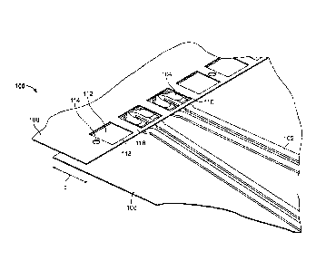
Referring now to FIG. 1, a first advantageous embodiment of an electrical
connection
interface 100 according to the present invention, is shown.
In Fig. 1, only the metallic parts, i. e. the signal leads and the ground
plane layers, are
shown in order to make clear the gist of the invention. However, of course,
also insulating
layers are present and furthermore, the shown metallic layers do not have to
be the only
electrically conductive layers. For instance, each printed circuit board may
contain
embedded active and passive components and, furthermore, also more than two
circuit
boards can be stacked, interconnecting same by means of more than one
electrical
connection interface 100.
According to a basic embodiment of the present invention as shown in Fig. 1,
the
electrical connection interface 100 is used for connecting two printed circuit
boards (PCB).
A first substrate (not shown in the figure) carries two pairs of first
electrically conductive
leads. On the substrate of a second PCB (not shown in the figure) second
electrically
conductive leads 104 are provided. The shown number of leads is of course only
intended
to give a particular example. Any other desired number of electrically
conductive leads is
of course also possible.
As shown in Fig. 1, on the first PCB there is arranged a first ground plane
layer 106. On
the opposing second PCB, there is provided a second ground plane layer 108.
Each of
these ground plane layers are either located within the printed circuit board
or situated on
a surface opposing to the one where the respective electrically conductive
leads 102, 104,
are arranged.
According to the present invention, the ground plane layers 106, 108 overlap
in the area
of the electrical connection interface 100, as indicated by the distance d.
The distance d
may have dimensions of about 1 mm, when assuming a solder ball size of 500
iirn x 200
urn x 80 urn. Each first electrically conductive lead 102 is connected to the
corresponding
second electrically conductive lead 104 by means of a solder ball 110.
However, when
providing an overlapping of the two ground plane layers 106, 108 according to
the present
invention, of course also other electrically conducting connection techniques,
such as
press fit pins can be used for connecting the signal leads. For establishing
the solder
CA 02891678 2015-05-13
WO 2014/082761
PCT/EP2013/063694
8
connection, each first and second electrically conductive lead 102, 104 has a
solder pad
structure in the interface region.
In the shown embodiment, adjacent to each differential pair of solder pads, a
clearance
112 is provided in the first ground plane layer 106. These clearances, which
sometimes
are also referred to as anti pads, are advantageously provided in order to
adjust the
differential impedance profile of the transmission lines. In Fig. 1, only two
pairs of first and
second electrically conductive leads 102, 104, are shown. However, there can
be of
course many more leads in parallel. In Fig. 1 an electrical connection between
the first
ground plane layer 106 and the second ground plane layer 108 is schematically
represented by the connection points 114. There may for instance be provided
solid
ground interconnects as connection points 114 between the first and second
ground plane
layers every forth differential pair of signal pads. The solder balls 110 may
have
dimensions of 500 pm x 200 pm x 80 pm.
Furthermore, the two leads of each pair of the first electrically conductive
leads 102 may
be distanced apart by 200 pm, whereas the adjacent pairs are distanced apart
for
instance by 350 pm. The first and second electrically conductive leads 102,
104, may
have a total length of for instance 11 mm and 3 mm, respectively.
As shown in Fig. 1, each of the clearances 112 is separated from an adjacent
one by
means of a grounding web 116 provided in the second ground plane layer 108.
Furthermore, a cross-talk suppression strip 118 is formed at the margin of the
second
ground plane layer 108. By using this particular design, a two-fold effect can
be achieved:
firstly a part of the second ground layer 108 is still present in the
interconnection area
providing an effect equal to an ESD shield. On the other hand, to achieve the
necessary
impedance match and therefore to avoid signal reflection, a cut-out is present
in a region
where the first and second electrically leads 102 and 104 are connected to
each other.
Therefore, cross-talk components can be blocked while still maintaining an
unaltered (or
only marginally different) differential impedance.
In Fig. 1, only the second ground plane layer 108 is provided with clearances
112.
However, of course additionally or alternatively such clearances can also be
provided in
the first ground plane layer 106.
Fig. 2 shows a second advantageous embodiment of the electrical connection
interface
100 according to the present invention. According to this embodiment, the
second ground
CA 02891678 2015-05-13
WO 2014/082761
PCT/EP2013/063694
9
plane layer 108 is modified in that each of the clearances 112 of Fig. 1 is
partitioned into
two clearances 112a and 112b by an additional grounding web 120. By
introducing such a
short strip of conducting line in the middle of the clearance 112 between the
two signal
pads, a further improvement to the common mode impedance and the mode
conversion
can be achieved. In particular, the additional grounding web 120 is widened in
the regions
of the traces 104, where they escape and diverge to the solder pads. Such a
tapered
region 122 reduces the self-inductance and thus improves the signal integrity.
With the arrangement of Fig. 2 the connection between the first ground plane
layer 106
and the second ground plane layer 108 may either be performed in a GSSSSG
configuration or a GSSG configuration. The first configuration with fewer
connection points
114 between the two ground plane layers has advantages in view of the
necessary space,
whereas providing more connection points is more advantageous in cases where
common
mode impedance, mode conversion and cross-talk are very critical.
In particular, Fig. 3 shows the more robust GSSG configuration with connection
points 114
provided between every second differential pair of signal pads.
Figs. 4 to 9 illustrate the actual performance of the arrangement according to
Fig. 1. In
particular, Fig. 4 shows a differential mode impedance profile from the side
of the first
electrically conductive leads 102 for a 15 ps 20% to 80% rise time at a
nominal
impedance of 90 O. The return loss corresponding to the impedance profile of
Fig. 4 is
shown in Fig. 5.
Return loss is a frequency domain parameter analogous to the time domain
impedance
profile. Return loss (RL) is defined as the amount of signal energy reflected
back towards
the source as a result of impedance mismatches in the transmission path.
Further, Fig. 6 shows the common mode impedance profile from the side of the
first signal
leads with a 15 ps 20% to 80% rise time for the embodiment of Fig. 1 at a
nominal
impedance of 22.5 O. Fig. 7 shows the return loss corresponding to the
impedance profile
of Fig. 6.
As already indicated above, cross-talk is often a critical parameter to
consider when
selecting an interconnect for a high speed application. Cross-talk can be
defined as noise
arising from unwanted coupling of nearby signal lines. It occurs when two
signals are
partially superimposed on each other by inductive and capacitive coupling
between the
CA 02891678 2015-05-13
WO 2014/082761
PCT/EP2013/063694
conductors carrying the signals. Cross-talk can result in distortion and
degradation of the
desired signals. There are two types of crosstalk of concern in high speed
systems, near
end (NEXT) and far end crosstalk (FEXT). NEXT is the measure of the level of
crosstalk
at the transmitting end of the signal path, while FEXT is the measure of
crosstalk at the
5 receiving end of the signal path.
Fig. 8 shows the near end cross-talk and the far end cross-talk for the
embodiment of Fig.
1 and Fig. 9 shows the mode conversion for the interconnect shown in Fig. 1.
In these
Figures, MS1 and MS2 signify the first and second electrically conductive
leads,
respectively. For the embodiment of Fig. 1, the insertion loss vs. cross-talk
ratio is about
10 47 dB at 14 GHz and 30 dB at 35 GHz. As this is known to a person
skilled in the art, a
value of 30 dB corresponds to the typical transceiver dynamic range.
The performance of the arrangement according to Fig. 3 is illustrated in the
measurement
curves of Figures 10 to 15. Specifically, Fig. 10 shows the differential mode
impedance
profile from the side of the first signal leads with a 15 ps 20% to 80% rise
time at a
nominal impedance of 90 C) for the embodiment shown in Fig. 32, and Fig. 11
shows the
return loss corresponding to the impedance profile of Fig. 10.
Further, Fig. 12 shows the common mode impedance profile from the side of the
first
signal leads with a 15 ps 20% to 80% rise time at a nominal impedance of 22.5
C) for the
embodiment of Fig. 3. and Fig. 13 shows the return loss corresponding to the
impedance
profile of Fig. 12.
Fig. 14 shows the near and far end cross-talk for the interconnect shown in
Fig. 3 and Fig.
15 shows the mode conversion for the interconnect shown in Fig. 3. For the
arrangement
according to Fig. 3, the insertion loss vs. cross-talk ratio is about 47 dB at
14 GHz and 30
dB for frequencies beyond 40 GHz.
Fig. 16 shows in a top view a further advantageous embodiment of the present
invention.
Again, a first printed circuit board is connected to a second substrate which
in contrast to
the previous embodiments of Figs. 1 to 3, however, is formed by a flexible
printed circuit
(FPC).
In Fig. 16 only the metallic parts are shown, in particular, the first ground
plane layer 106'
and the second ground plane layer 108' as well as the first and second
electrically
conductive leads 102' and 104', respectively. Similar to the embodiments shown
in Figs. 1
CA 02891678 2015-05-13
WO 2014/082761
PCT/EP2013/063694
11
to 3, clearances 112' are provided in the second ground plane layer 108' for
performing an
optimized impedance matching. In contrast to the previous embodiments,
however, the
connection points 114' between the first and second ground plane layers (106',
108') are
not arranged in close vicinity of the clearances, but at a remote location
formed by
protruding fingers 124. This design also implies a much larger overlap
distance d'.
The advantage of this particular embodiment can mainly been seen in the fact
that a much
more narrow design can be achieved. Furthermore, the mechanical stability of
the FPC
carrying the second ground plane layer 108' is enhanced thereby. The design
according
to Fig. 16 may advantageously be used for an FPC to PCB interconnect that is
able to
connect 12 channels transmitting data rates of 25 Gbps with a still
satisfactory signal
integrity.
The actual performance of the arrangement according to Fig. 16 is illustrated
in the
measurement curves of Figures 17 to 23. Specifically, Fig. 17 shows the
differential mode
impedance profile from the FPC side with a 15 Ps 20% to 80% rise time and a
nominal
impedance of 90 for the embodiment shown in Fig. 16, and Fig. 18 shows the
return
loss corresponding to the impedance profile of Fig. 17.
Fig. 19 shows the common mode impedance profile from the FPC side with a 15 ps
20%
to 80% rise time and a nominal impedance of 22.5 C) for the embodiment shown
in Fig.
16, and Fig. 20 shows the return loss corresponding to the impedance profile
of Fig. 19.
Fig. 21 shows the near end and far end cross talk for the interconnect shown
in Fig. 16,
and Fig. 22 shows the mode conversion for the interconnect according to the
embodiment
shown in Fig. 16. For the embodiment according to Fig. 16, the insertion loss
vs. cross-
talk ratio is about 49 dB at 14 GHz and 30 dB at 33 GHz.
The principles of the present invention can advantageously be employed with
electro-
optical engines (E/O engines), i. e. conversion components which transform
electrical
signals into optical signals and vice versa. Such E/O engines can be coupled
to optical
fibers on the one hand and electrical leads on the other hand and light
emitting as well as
light receiving elements for performing the desired conversion between the
electrical and
optical domain.
Intensive research has shown that only very specific values for the overlap
between the
printed circuit board and such an E/O engine circuit carrier lead to
satisfying results in all
CA 02891678 2015-05-13
WO 2014/082761
PCT/EP2013/063694
12
decisive characteristics. In particular, the signal integrity performance,
that is, the
differential and common mode return loss as well as the crosstalk and mode
conversion,
has to be sufficiently high. On the other hand, there should be left enough
space for the
E/O engine, in particular for the IC and the optoelectronic components as well
as the
necessary thermally conductive material. It could be shown that an overlap
distance d in a
range between 0.5 and 0.8 mm yields the best results.
Fig. 23 shows an example of a layout diagram of an E/O engine mounted to a
printed
circuit board. The E/O engine circuit carrier is mounted over a rectangular
cut out of a
printed circuit board and the edge 126 of the PCB is indicated by a broken
line in the
drawing. In the configuration of Fig. 23, a GSSSG configuration is chosen,
meaning that
always three pairs of differential signal lines are separated by one ground
line.
An important parameter to be considered is firstly the minimum distance
between the
differential signal pairs indicated by reference sign a. This distance has to
be at least 0.25
mm in order to ensure sufficient signal integrity. Furthermore, the distance b
between two
grounding points has to be less than 3.5 mm. Regarding the overlap distance d
it could be
shown that same should be within the range of 0.5 and 0.8 mm. These particular
distances are also highlighted in the schematic detail of Fig. 23 shown in
Fig. 24.
Fig. 25 shows a further embodiment of the present invention, in particular an
E/O engine,
where the signal pairs are arranged in a GSSG configuration, wherein always
two pairs of
signals are separated by one ground connection. As shown in Fig. 25, the E/0
engine
component 128 comprises an integrated circuit (IC) with drivers 130, an IC
comprising
vertical cavity surface emitting lasers (VSCEL) 132, and transimpedance
amplifiers (TIA)
134. Furthermore, optical receivers 136, in particular PIN optical receivers,
are provided
for the conversion of received optical signals into electric signals.
The transmitting differential front end lines 138 and the receiver
differential front end lines
140 are arranged in the already mentioned GSSG configuration. Furthermore,
vias 142
are provided to connect an additional metal layer. In this particular example,
the E/O
engine component 128 has for instance dimensions of 9 mm x 10 mm. For this
particular
application, the distance a between two differential signal pairs has to be at
least 0.2 mm.
Further, the distance b between two ground connections has to be at least 2.5
mm, as
indicated in Fig. 25.
CA 02891678 2015-05-13
WO 2014/082761 PCT/EP2013/063694
13
The use of the terms "a" and "an" and "the" and similar referents in the
context of
describing the invention (especially in the context of the following claims)
are to be
construed to cover both the singular and the plural, unless otherwise
indicated herein or
clearly contradicted by context. The terms "comprising," "having,"
"including," and
"containing" are to be construed as open-ended terms (i.e., meaning
"including, but not
limited to,") unless otherwise noted. Recitation of ranges of values herein
are merely
intended to serve as a shorthand method of referring individually to each
separate value
falling within the range, unless otherwise indicated herein, and each separate
value is
incorporated into the specification as if it were individually recited herein.
All methods
described herein can be performed in any suitable order unless otherwise
indicated herein
or otherwise clearly contradicted by context. The use of any and all examples,
or
exemplary language (e.g., "such as'') provided herein, is intended merely to
better
illuminate the invention and does not pose a limitation on the scope of the
invention
unless otherwise claimed. No language in the specification should be construed
as
indicating any non-claimed element as essential to the practice of the
invention.
CA 02891678 2015-05-13
WO 2014/082761
PCT/EP2013/063694
14
Reference Numerals
Reference Numerals Description
100, 100' electrical connection interface
102, 102' first electrically conductive lead
104, 104' second electrically conductive lead
106, 106' first ground plane layer
108, 108' second ground plane layer
110 solder ball
112, 112' clearance
114, 114' connection point
116 grounding web
118 grounding strip for cross-talk suppression
120 additional grounding web
122 tapered region of additional grounding
web
124 protruding contact finger
d, d' overlap distance
126 edge of PCB
a distance between two signal pairs
distance between two grounding points
128 E/O engine component
130 drivers
132 VCSELs
134 TIAs
136 PINs
138 Tx differential lines
140 Rx differential lines
142 vias