Note: Descriptions are shown in the official language in which they were submitted.
CA 02892385 2015-05-21
WO 2014/082092
PCT/US2013/072085
MULTI-PANE WINDOWS INCLUDING ELECTROCHROMIC
DEVICES AND ELECTROMECHANICAL SYSTEMS DEVICES
CROSS-REFERENCE TO RELATED APPLICATION
[0001] This is a non-provisional application of, and claims priority to, U.S.
Provisional
Patent Application No. 61/729,987 entitled "MULTI-PANE WINDOWS INCLUDING
ELECTROCHROMIC DEVICES AND ELECTROMECHANICAL SYSTEMS DEVICES,"
filed on 11/26/2012, which is hereby incorporated by reference in its entirety
for all purposes.
FIELD OF INVENTION
[0002] The invention relates generally to multi-pane windows, and more
particularly to
multi-pane windows including electrochromic devices and electromechanical
systems
devices.
BACKGROUND
[0003] Electrochromism is a phenomenon in which a material exhibits a
reversible
electrochemically-mediated change in an optical property when placed in a
different
electronic state, typically by being subjected to a voltage change. The
optical property is
typically one or more of color, transmittance, absorbance, and reflectance.
One well known
electrochromic material, for example, is tungsten oxide (W03). Tungsten oxide
is a cathodic
electrochromic material in which a coloration transition, transparent to blue,
occurs by
electrochemical reduction.
[0004] While electrochromism was discovered in the 1960s, electrochromic
devices still
unfortunately suffer various problems and have not begun to realize their full
commercial
potential. Electrochromic materials may be incorporated into, for example,
windows and
mirrors. The color, transmittance, absorbance, and/or reflectance of such
windows and
mirrors may be changed by inducing a change in the electrochromic material.
However,
advancements in electrochromic technology, apparatus, and related methods of
making
and/or using them, are needed because conventional electrochromic windows
suffer from, for
example, high defectivity, and low versatility.
1
CA 02892385 2015-05-21
WO 2014/082092
PCT/US2013/072085
BRIEF DESCRIPTION OF THE DRAWINGS
[0005] The following detailed description can be more fully understood when
considered in
conjunction with the drawings in which:
[0006] Figure 1 depicts a perspective exploded view of a multi-pane window
unit.
[0007] Figure 2A depicts a cross-section of a multi-pane window unit.
[0008] Figures 2B and 2C depict cross-sections of multi-pane window units
employing
laminate panes.
[0009] Figure 3A is a schematic cross-section of a multi-pane window unit.
[0010] Figure 3B is a partial cross section of an insulated glass unit showing
relative
configurations of substrates, electrochromic device, bus bar, spacer, primary
seal and the
secondary seal.
[0011] Figure 4 is a schematic cross-section of an electrochromic device.
[0012] Figure 5 is a schematic cross-section of an electrochromic device in a
bleached state.
[0013] Figure 6 is a schematic cross-section of an electrochromic device in a
colored state.
[0014] Figure 7 is a schematic cross-section of an electrochromic device
having an ion
conducting electronically insulating interfacial region rather than a distinct
ionically
conductive (also called "IC") layer.
SUMMARY
[0015] Multi-pane laminates having electrochromic devices and
electromechanical systems,
multi-pane window units having electrochromic devices and electromechanical
systems,
single panes having electrochromic devices and electromechanical systems, and
methods of
fabricating components thereof.
[0016] One embodiment is directed to a window unit having a first
substantially transparent
substrate having an electrochromic device disposed thereon, a second
substantially
transparent substrate having an array of electromechanical systems devices,
and a separator
between the first and second substantially transparent substrates. In one
case, the separator
2
CA 02892385 2015-05-21
WO 2014/082092
PCT/US2013/072085
includes a spacer and a seal between the spacer and each of the first and
second substantially
transparent substrates to seal an interior region.
[0017] One embodiment is directed to an insulating glass unit comprising a
first pane having
an electrochromic device disposed thereon, a second pane having an array of
electromechanical systems devices, and a sealing separator defining, together
with the first
and second panes, an interior region that is thermally insulating. In one
case, the insulating
glass unit further comprises a controller configured to control two or more
optical states of
the electrochromic device and/or to control the actuated and non-actuated
states of the array
of electromechanical systems devices.
[0018] One embodiment is directed to a method of changing between multiple
optical states
in a window unit including a first substantially transparent substrate having
an electrochromic
device disposed thereon and a second substantially transparent substrate
having an array of
electromechanical systems devices. The method comprises changing optical state
of the
electrochromic device without changing optical state of the array of
electromechanical
systems devices and changing optical state of the array of electromechanical
systems devices
without changing optical state of the electrochromic device.
[0019] One embodiment is directed to a method of fabricating a window unit.
The method
comprises arranging, substantially parallel to each other, a first
substantially transparent
substrate with an electrochromic device disposed thereon and a second
substantially
transparent substrate with an array of electromechanical systems devices. The
method further
comprises providing a sealing separator between the first and second
substantially transparent
substrate.
[0020] One embodiment is directed to a method of fabricating an insulating
glass unit. The
method comprises arranging a first pane of architectural glass and a second
pane of
architectural glass in a substantially parallel arrangement, wherein the first
pane includes an
electrochromic device disposed thereon, and the second pane includes an array
of
electromechanical systems devices, providing a sealing separator between the
first and
second panes, the sealing separator defining, together with the first and
second panes, a
thermally-insulating interior region between the first and second panes, and
charging the
thermally-insulating interior region with an inert gas.
3
CA 02892385 2015-05-21
WO 2014/082092
PCT/US2013/072085
[0021] One embodiment is directed to a multi-pane window unit comprising a
first pane, a
second pane, and an array of electromechanical systems devices disposed on the
second pane.
The second pane is laminated to the first pane. In one case, the multi-pane
window unit
further comprises a third pane and a separator between the third pane and the
laminated first
and second panes. In one case, the electrochromic device has at least two
optical states and
the array of electromechanical systems devices has two states.
[0022] One embodiment is directed to a multi-paned laminate comprising a first
pane, a
second pane laminated to the first pane, and an array of electromechanical
systems devices
disposed on an outward facing surface of the second pane. In one case, the
second pane is
laminated to the first pane with a lamination adhesive therebetween. In one
case, the multi-
paned laminate further comprises an electrochromic device disposed on the
second pane.
[0023] Certain embodiments are directed to a substantially transparent
substrate comprising a
first side, a second side opposing the first side, an electrochromic device
disposed on the first
side, and an array of electromechanical systems devices disposed on one of the
first and
second sides. In one case, the array of electromechanical systems devices is
disposed on the
same side as the electrochromic device. In certain cases, the array of
electromechanical
systems devices is disposed in tandem with the electrochromic device.
DETAILED DESCRIPTION
[0024] Herein are described window units (e.g. certain insulating glass units
also referred to
as IGUs) that have at least two panes, one pane having an electrochromic
device disposed
thereon and one pane having an array of microelectromechanical systems (MEMS)
devices or
other electromechanical systems (EMS) devices disposed thereon. These window
units may
have at least four optical states. For example, when each pane of the window
unit has two
optical states, then the window unit may have four optical states. In various
embodiments,
window units described herein allow the window user a greater choice of how
much light is
transmitted through the window, that is, the multi-pane window with EMS
devices allows a
gradation of transmission rather than the two optical states of a simple two-
state
electrochromic window. In certain embodiments, EMS devices are included with
electrochromic devices that can vary light transmission beyond two states. A
secondary
benefit is the improvement in defectivity due to non-aligned optical defects.
Another benefit
may be increased speed in transition. Other benefits of certain embodiments
are discussed
elsewhere in the disclosure.
4
CA 02892385 2015-05-21
WO 2014/082092
PCT/US2013/072085
[0025] Certain embodiments are described in relation to low-defectivity all
solid state and
inorganic electrochromic devices, however, the invention is not limited in
this way. Virtually
any electrochromic device or devices can be used in combination with virtually
any array of
MEMS devices or other EMS devices.
[0026] One of ordinary skill in the art would appreciate that the term "two-
state" in two-state
electrochromic device refers to the bleached state and the colored state, each
of which
requires an applied current and/or voltage. In actuality, a two-state
electrochromic device
will have three states: bleached, colored and neutral. "Neutral" describes the
'natural' state
of the window when no charge is applied to either bleach or color the device.
For example,
Figure 4 shows a two-state electrochromic device in a neutral state, while
Figures 5 and 6
show bleached and colored states, respectively. For the purposes of this
application, "states"
of an electrochromic device are assumed to be colored or bleached states
achieved by
application of current and/or voltage to the electrochromic device, although
neutral states are
inherent to electrochromic devices. Although certain embodiments describe two-
state
electrochromic devices, electrochromic devices with more than two states can
be used. For
example, electrochromic devices having four or more optical states can be
used, these optical
states can be distinct end states or the electrochromic device can have
variable-state
capability.
[0027] In certain embodiments, arrays of EMS devices have two states, an
actuated state and
an unactuated state. In some embodiments, the actuated state may render the
array of EMS
devices substantially opaque and the unactuated state may render the array of
EMS devices
substantially transparent, or vice versa. The actuated and unactuated states
may also switch
between substantially reflective (or absorptive) and substantially
transparent, for example.
Other states are also possible when the array of EMS devices is in an actuated
or unactuated
state. For example, microshutters, a type of MEMS device, may be fabricated
from a tinted
(but non-opaque) coating, which when shut provide a tinted pane, and when open
the tint is
substantially removed. Further, some arrays of EMS devices may have three,
four, or more
states that are able to be transitioned to. In some cases, the EMS devices can
modify visible
and/or infrared transmission. The EMS devices may reflect in some cases, may
be absorptive
in other cases, and in yet other embodiments may provide both reflective and
absorptive
properties. In certain embodiments, the EMS devices may be operated at
variable speeds,
e.g., to transition from a high transmission state to a low-transmission
state, or a no-
transmission state. In certain cases, the EMS devices may be used in
conjunction with an
5
CA 02892385 2015-05-21
WO 2014/082092
PCT/US2013/072085
electrochromic device as a temporary light blocking measure, e.g., to block
light until the
associated electrochromic device has transitioned to a lower transmissivity
state or a higher
transmissivity state.
[0028] Examples of arrays of EMS devices include microblinds and microshutters
arranged
in an array. Microblinds and microshutters and their methods of fabrication
are described
respectively in U.S. Patent No. 7,684,105 and U.S. Patent No. 5,579,149, both
of which are
hereby incorporated by reference in their entirety.
[0029] In some embodiments, each EMS device may include a portion attached to
the
substrate (e.g., a hinge or an anchor) and a mobile portion. When actuated by
electrostatic
forces, the mobile portion may move and obscure the substrate. In the
unactuated state, the
mobile portion may expose the substrate. In the example of some microblinds,
the mobile
portion may be an overhanging portion of a material layer that curls when
actuated by
electrostatic forces. In the example of some microshutters, the mobile portion
can rotate or
curl when actuated. In some cases, the EMS devices may be actuated and
controlled by
electrostatic control means. In the example of microshutters, the
electrostatic control means
may control the angle of rotation or curl to different states. The substrate
with the array of
EMS devices may also include a conductive layer. In the example of
microblinds, the
microblinds are fabricated using a thin layer(s) under controlled stress.
[0030] In certain embodiments, the EMS devices may have different power
requirements,
and in such cases a controller is configured to power and control the EMS
devices
independently from the electrochromic device. For example, one pane of a
window unit or
IGU has an electrochromic device coating thereon, and another pane of the same
window unit
or IGU has an EMS device system thereon. A controller is configured to deliver
the
powering needs of each lite independently of the other. An electrochromic
device may
require a few volts to operate, while an EMS device may in some instances
require larger
voltages in order to establish sufficient potential to physically move the EMS
device
feature(s) to operate it.
[0031] The array of EMS devices may be provided over any suitable portion of
the
substantially transparent substrate. In many embodiments, the array of EMS
devices is
provided over the portion of the substantially transparent substrate that
receives light.
6
CA 02892385 2015-05-21
WO 2014/082092
PCT/US2013/072085
[0032] Multi-pane electrochromic windows are described in U.S. Patent
Application serial
number 12/851,514 (now U.S. Patent No. 8,270,059), entitled "Multi-Pane
Electrochromic
Windows," filed on August 05, 2010 and naming Robin Friedman et al. as
inventors, which is
hereby incorporated by reference in its entirety. Aspects of the multi-pane
window units
disclosed herein, which include an electrochromic device and an array of EMS
devices may
be similar to the multi-pane electrochromic windows described in the
12/851,514 application.
MULTI-PANE WINDOWS
[0033] In certain embodiments, a "window unit" can refer to an assembly with
one or more
substantially transparent substrates (sometimes referred to herein as panes).
In one
embodiment, a window unit may include two substantially transparent substrates
(e.g., two
panes of glass) where a first substrate has at least one electrochromic device
disposed
thereon, and a second substrate has an array of EMS devices disposed thereon.
In another
embodiment, a window unit may include two substantially transparent substrates
where one
of the substrates has an electrochromic device disposed on one surface and an
array of EMS
devices disposed on an opposing surface. In another embodiment, a window unit
may
include a single substantially transparent substrate having an electrochromic
device disposed
on one surface and an array of EMS devices disposed on the same or an opposing
surface. In
yet another embodiment, a window unit may include three substantially
transparent
substrates. In this embodiment, one or more electrochromic devices may be
disposed on
surfaces of one or more of the substrates, and an array of EMS devices may be
disposed on
one or more of the other surfaces that do not have an electrochromic device
disposed thereon.
In embodiments of window units with multiple panes, certain embodiments may
have an
array of EMS devices on a surface facing the inside of the building or the
room, or facing the
interior region of an IGU, for example, in order to protect by the inert dry
environment.
[0034] In certain embodiments, the substantially transparent substrates of a
multi-pane
window unit have a separator (sometimes referred to herein as a "spacer")
disposed between
them. Since an IGU may include more than two substrates assembled into a unit,
and
electrochromic devices and arrays of EMS devices specifically may include
electrical leads
for connecting the devices to a voltage source, a current source, switches,
and the like, the
term "window unit" may be used herein to convey a more simple assembly. That
is, for the
purposes of this disclosure, an IGU of certain embodiments may include more
components
than a window unit. In certain embodiments, the most basic assembly of a
window unit
7
CA 02892385 2015-05-21
WO 2014/082092
PCT/US2013/072085
includes two substrates, each with an electrochromic device thereon, and a
sealing separator
in between and registered with the two substrates. In one embodiment, an all
solid state low-
defectivity electrochromic device on a first substrate of a multi-pane window
unit and an
array of EMS devices on a second substrate of a multi-pane window unit are
employed
opposing each other in an IGU.
[0035] One embodiment is directed to a window unit including: a first
substantially
transparent substrate and an electrochromic device disposed thereon; a second
substantially
transparent substrate and an array of EMS devices disposed thereon; and a
sealing separator
between the first and second substantially transparent substrates, which
sealing separator
defines, together with the first and second substantially transparent
substrates, an interior
region that may be thermally insulating. Figure 1 depicts a window unit, 100,
having a first
substantially transparent substrate, 105, a separator, 110, and a second
substantially
transparent substrate, 115. Substrate 105 has an electrochromic device
fabricated thereon.
Substrate 115 has an array of EMS devices fabricated thereon. When the three
components
are combined, where separator 110 is sandwiched in between and registered with
substrates
105 and 115, window unit 100 is formed. Window unit 100 has an associated
interior space
defined by the faces of the substrates in contact with the separator and the
interior surfaces of
the separator. Separator 110 is typically a sealing separator, that is, it
includes a spacer and a
seal between the spacer and each substrate where they adjoin in order to
hermetically seal the
interior region for protecting the interior region from moisture intrusion and
the like.
[0036] As a convention, for two-pane window units described herein, the four
viewable
surfaces of the two substrates may be referenced numerically. Surface 1 is the
surface of a
substrate that faces outside, for example, outside a room or a building having
such window
unit installed in a window in a wall thereof. Surface 2 is the opposing
surface of the substrate
that faces inside the interior space. Surface 3 is the surface of the second
substrate that faces
inside the interior space of the window unit. Surface 4 is the opposing
surface of the second
substrate that faces outside the interior space of the window unit but inside,
for example, the
aforementioned room or building. This convention does not negate using window
units
described herein for entirely interior spaces of buildings; however, there are
particular
advantages to using them on exterior walls of buildings because of their
optical as well as
thermally-insulating properties.
8
CA 02892385 2015-05-21
WO 2014/082092
PCT/US2013/072085
[0037] "Substantially transparent substrates" include those described herein
in relation to
substrates for electrochromic devices (e.g., solid-state inorganic
electrochromic devices) and
arrays of EMS devices. That is, they are substantially rigid substrates made
of substantially
transparent material such as, for example, glass or plexiglass. The
substantially transparent
substrates of a window unit need not be made of the same material, for
example, one
substrate may be plastic while the other may be glass. In another example, one
substrate may
be thinner than the other substrate, for example, the substrate that would
face the interior of a
structure, which is not exposed to the environment, may be thinner than the
substrate that
would face the exterior of the structure. In one embodiment, the
electrochromic device
proximate the exterior environment, for example, the exterior of a building,
may be better
able to withstand environmental degradation than the array of EMS devices,
which are
proximate the interior of the building. In one embodiment, at least one of the
first and second
substantially transparent substrates includes architectural glass. In another
embodiment, at
least one of the first and second substantially transparent substrates further
includes a low
emissivity coating. In another embodiment, at least one of the first and
second substantially
transparent substrates further includes an ultraviolet (UV) and/or infrared
(IR) absorber,
and/or, a UV and/or IR reflective layer. In one embodiment, the UV and/or IR
reflective
and/or absorber layer is on at least surface 1, in another embodiment on
surface 2, in yet
another embodiment on at least surface 3, and in another embodiment on at
least surface 4.
In these embodiments, "on" a surface means on or associated with, considering
that such
layers or coatings may be either in direct contact with the surface of the
substrate and/or on
top of, for example, the EC stack or array of EMS devices that is disposed on
the surface of
the substrate. One embodiment is any window unit described herein where the
electrochromic device has an UV and/or IR absorber and/or a UV and/or IR
reflective layer
thereon.
[0038] The electrochromic device may include one or more transparent
conductive oxide
layers in some embodiments. In one embodiment, at least one of the transparent
conductive
oxide layers of the electrochromic device is a heatable transparent conductive
oxide layer
configured so that it can be heated via application of electricity
independently of operation of
the electrochromic device of which it is a part. This may be useful for a
number of reasons
such as, for example, to preheat the electrochromic device prior to
transitioning and/or to
create an insulating barrier to ameliorate heat loss from the interior of a
building. Thus, one
embodiment is a window unit as described herein, where the window unit
includes an
9
CA 02892385 2015-05-21
WO 2014/082092
PCT/US2013/072085
electrochromic device having one or more transparent conductive oxide layers,
where one of
the transparent conductive oxide layers of the electrochromic device is
configured so that it
can be heated via application of electricity independently of operation of the
electrochromic
device of which it is a part. One embodiment is a two-pane window unit as
described herein,
where on pane has an electrochromic device on its surface facing the interior
region (e.g.,
surface 2) and a transparent conductive oxide layer of the electrochromic
device on surface 2,
where the transparent conductive oxide layer is configured for heating via
application of
electricity and where the application of electricity for heating can be
independent of
operation of the electrochromic device. In certain embodiments, the substrate
with EMS
devices may have a heatable transparent conductive oxide layer. This may be
desirable, e.g.,
to warm the EMS devices which may improve facile movement of the devices'
features.
[0039] In one embodiment, the electrochromic device is all solid-state and
inorganic, and in
another embodiment the electrochromic device is also a low-defectivity device,
for example,
a low-defectivity all solid-state and inorganic electrochromic device.
[0040] The electrochromic device and the array of EMS devices need not
necessarily face
each other in the interior region of the window unit (for example, on surfaces
2 and 3), but in
one embodiment they do. This configuration is desirable because both the
electrochromic
device and the array of EMS devices are protected from the outside environment
and may be
in a sealed interior region of the window unit. It is also desirable for the
electrochromic
device and the array of EMS devices to extend over substantially the entire
viewable region
of the substantially transparent substrate on which they reside.
[0041] Figure 2A depicts a cross-section of a window unit, 200, which includes
a first pane,
205, (e.g., architectural glass pane) with an electrochromic device, 210,
disposed thereon.
Window unit 200 also includes a second pane, 215, (e.g., architectural glass
pane) with an
array of EMS devices, 220, disposed thereon. Devices 210 and 220 face each
other in the
interior region of window unit 200. A sealing separator, 225, seals the window
unit, and in
this example, overlaps a portion of the electrochromic device. Electrical
connections (not
shown) might also pass through, or otherwise contact, separator 225. Separator
225 may
have a unitary body or may be made of multiple parts, for example, a rigid or
semi-rigid
spacer and one or more adhesive or other sealing elements. In one example,
separator 225
includes a spacer (e.g., a metal spacer) and two seals that seal the areas
where the spacer
adjoins to each of the panes, sometimes referred to as primary seals, and
another seal around
CA 02892385 2015-05-21
WO 2014/082092
PCT/US2013/072085
the outer perimeter of the spacer, and between the panes, sometimes called a
secondary seal,
which may be made of, for example, a sealing adhesive. Separator 225 is
simplified for the
purposes of the illustration in Figure 2A.
[0042] In the stylized figure of Figure 2A, array of EMS devices 220 is
depicted as a single
layer that does not touch, or extend under, separator 225. In certain
embodiments, the
electrochromic device has no moving parts, only ions that move within the EC
device during
operation. In certain embodiments, the EMS devices have moving parts (e.g.,
microshutters)
that cannot be physically blocked from movement in order to fully operate. In
certain
embodiments, the array of EMS devices may come very close to the separator,
and there may
also be a tinted material, in some embodiments the same material coating(s)
from which the
EMS device array is constructed, around the perimeter of the EMS device array
so as to block
light around the periphery.
[0043] Due to the higher temperatures (e.g., higher temperature due to
absorption of radiant
energy by an electrochromic device and/or an array of EMS devices on the
panes) that multi-
pane window units may experience, more robust separators and sealants than
those used in
conventional IGUs may be used in certain embodiments.
[0044] In illustrated examples, sealing separator 225 is disposed about
peripheral regions of
the first and second substantially transparent substrates without
substantially obscuring a
viewable region of the window unit (also, for example, as depicted in Figure
1) away from
the peripheral regions. In one embodiment, the sealing separator 225
hermetically seals the
interior region of the window unit. The interior region of the window unit is
typically, but
not necessarily, charged with an inert gas such as argon or nitrogen, xenon,
or krypton. In
one embodiment, the interior space is substantially liquid free. In one
embodiment, the
interior space is charged with an inert gas and substantially liquid free. In
one embodiment,
the interior space is substantially moisture-free, that is, for example,
having a moisture
content of less than about <0.1 ppm. In another embodiment, the interior space
would require
at least about -40 C to reach dew point (condensation of water vapor from the
interior space),
in another embodiment at least about -70 C. In certain cases, the gas mixture
(at pressure or
partial vacuum) in the interior region of window unit may be configured to aid
in switching
of the EMS device array.
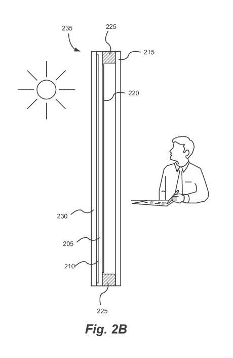
[0045] Figure 2B depicts a cross-section of a window unit, 235, which includes
a first pane,
230, with an electrochromic device, 210, disposed thereon. Window unit 235
also includes a
11
CA 02892385 2015-05-21
WO 2014/082092
PCT/US2013/072085
second pane, 205, with an array of EMS devices, 220, disposed thereon. In this
embodiment,
panes 230 and 205 are laminated to each other. Devices 210 and 220 do not face
each other,
and array of EMS devices 220 is in the interior region of window unit 235. A
sealing
separator, 225, seals the window unit 235. A third pane, 215, is registered
with and opposite
of the laminate construct. Third pane 215 may also have a passive or active
coating thereon
(not shown). Electrical connections (not shown) might also pass through, or
otherwise
contact, separator 225. Separator 225 may include features as described above
in relation to
Figure 2A. Since it is protected by pane 230, pane 205 may be annealed glass
(e.g., thin,
flexible, annealed glass having a thickness of about 3.2 mm to about 0.05 mm
as is
commercially available). One advantage of having both an electrochromic device
and an
array of EMS devices on a single laminate as, for example, depicted in Figure
2B, is that the
construct is less complex, only the outer pane heats up significantly during
absorption, and
annealed glass, particularly thin annealed glass, can be used as a substrate
for the EMS device
array. Of course, the construct described in relation to Figure 2B need not be
deployed with
the absorptive (laminated) pane on the outward side, instead it may be on an
inward side,
although the outward side configuration may be desirable in some instances.
[0046] One embodiment is directed to a two-paned laminate including an
electrochromic
device and an EMS device array. In one case, the EMS device array is on a
first pane and the
electrochromic device is on a second pane, where the electrochromic device is
laminated
between the panes and the EMS device array is on the surface opposite the
lamination
adhesive. In another case, the EMS device array is on a first pane and the
electrochromic
device is on the same first pane, where a second pane is laminated to the
first pane, and the
electrochromic device is between the panes (touching the lamination adhesive)
and the EMS
device array is opposite the lamination adhesive.
[0047] Another embodiment is a single pane including an EC device on one side
and an EMS
device array on the opposite side. The side with the EC device may be
laminated to another
pane. If laminated, the laminate may serve as one pane of a dual or triple
pane IGU or
window unit. If unlaminated, the single pane may serve as the central pane of
a triple pane
window unit or IGU.
[0048] Certain embodiments are directed to a substantially transparent
substrate having an
electrochromic device disposed on one side and an array (e.g., one dimensional
array or two-
dimensional array) of EMS devices disposed on the same or on an opposing side.
In one
12
CA 02892385 2015-05-21
WO 2014/082092
PCT/US2013/072085
embodiment, this substantially transparent substrate with the electrochromic
device and array
of EMS devices may be part of a laminate, where an additional transparent
substrate is
adhered to the side of the substantially transparent substrate bearing the EC
device so as to
protect it from environment. In this embodiment, the EMS device is housed
within the sealed
volume of the window unit so as to protect it from the environment. In another
embodiment,
the substantially transparent substrate with the electrochromic device and
array of EMS
devices on opposing surfaces may be located within a window unit, e.g. as a
middle pane of a
triple pane IGU.
[0049] Figure 2C depicts a cross-section of a window unit, 240, which includes
a first pane,
230, laminated to a second pane 205 as described above in relation to Figure
2B, but in this
embodiment, a third pane 215 has an electrochromic device 210 disposed
thereon. An array
of EMS devices, 220, is disposed on the second pane, 205. Devices 210 and 220
face each
other in the interior region of window unit 240. A sealing separator, 225,
seals the window
unit 240. First pane 230 may also have a passive or active coating thereon in
certain cases.
Electrical connections (not shown) might also pass through, or otherwise
contact, separator
225. Separator 225 may include features as described above in relation to
Figure 2A. Since
it is protected by first pane 230, second pane 205 may be annealed glass such
as flexible thin
annealed glass as may be commercially available and having a thickness of, for
example,
about 3.2 mm to about 0.05 mm. The construct described in relation to Figure
2C need not
be deployed with the laminated panes outwards. For example, in one embodiment,
the
construct described in relation to Figure 2C may be deployed in the opposite
orientation so
that the electrochromic device's absorptive properties may protect the EMS
devices from the
sun's radiation.
[0050] In certain embodiments, the electrochromic device is a two-state
electrochromic
device and the array of EMS devices is a two-state array. In these
embodiments, the window
unit has four optical states. In one such embodiment, the window unit, when
mounted, will
have a first substantially transparent substrate having a surface facing
outside a room or
building and a second substantially transparent substrate having a surface
facing inside the
room or building. In this embodiment, both the electrochromic device and array
of EMS
devices have their own high transmissive state and low transmissive state and
the
transmissivity of the low transmissive state of the array of EMS devices' is
higher than the
transmissivity of the low transmissive state of the electrochromic device. In
this context, the
transmissivity of the "device," i.e. transmissivity of either the
electrochromic device or array
13
CA 02892385 2015-05-21
WO 2014/082092
PCT/US2013/072085
of EMS devices, means the transmissivity of either the device itself or the
combination of the
transmissivity of the device and the substrate upon which the device is
disposed upon. That
is, for example, most substantially transparent substrates have inherent
absorptive properties,
for example, float glass alone typically has a transmissivity of about 92%.
[0051] One reason that it may be desirable to have transmissivity of the
electrochromic
device's low transmissive state lower than the transmissivity of the array of
EMS device's
low transmissive state is that when the electrochromic device is proximate the
exterior, it can
block more light (and therefore heat) transmission and thus ease the
requirements of the array
of EMS devices that may be more proximate the interior. For example, the
electrochromic
device with the higher transmissivity in its low transmissive state can filter
out a good portion
of the solar spectrum to protect the array of EMS devices from degradation as
compared to a
device without such protection.
[0052] In one embodiment, the array of EMS devices is proximate the exterior
and the
electrochromic device is proximate the interior. Depending on the material
construction of
the EMS devices, this configuration may allow the EMS devices array to protect
the
electrochromic device, and thus work well with a less robust electrochromic
device when
used in tandem with the EMS device array.
[0053] Another advantage to a multi-pane window unit, for example, a two-pane
window
unit with a device (e.g., electrochromic device or array of EMS devices) on
each pane, may
be that neither device need have stringent lower transmissivity, for example
less than 10%
transmissivity, because the net transmissivity through the window unit is a
product of both
electrochromic device and EMS devices transmissivity. An advantage of having
an
electrochromic device in addition to EMS devices may be that the
electrochromic device can
be thinner than it would otherwise be if the window unit had, and relied on,
only the
electrochromic device. A thinner electrochromic device translates into less
materials being
used which saves in manufacturing costs. A thinner electrochromic device may
also translate
into faster response times during transition, which may save operational cost
and energy, for
example, by using less electricity and controlling heat load entering a room
more quickly, and
may make a more attractive window for the end user because they absorb less
light in the un-
tinted state.
[0054] Another embodiment is a four-state multi-pane window unit. In one
embodiment, the
four-state window unit has two panes, one pane with two-state electrochromic
device and one
14
CA 02892385 2015-05-21
WO 2014/082092
PCT/US2013/072085
pane with a two-state array of EMS devices. By virtue of each pane having a
high and a low
transmissivity state, when combined, the multi-pane window has four possible
states.
[0055] Another embodiment is directed to a multi-pane window unit having at
least four
optical states. This multi-pane window unit has two or more panes. One of the
panes has a
substantially transparent substrate with an electrochromic device disposed
thereon, where the
electrochromic device has at least two (e.g., 2, 3, 4, 5, 6, 7, 8, etc.)
optical states. The other
pane has an array of EMS devices having at least two optical states. When
combined, there
are at least four possible optical states in this multi-pane window unit.
[0056] The transmissivity values of a two-pane window unit of one embodiment
are
provided in Table 1. In this embodiment, the electrochromic device and the
array of EMS
devices have two-states, on and off, each corresponding to low and high
transmissive states,
respectively. For example, the array of EMS devices has a high transmissivity
of 80% at a
high transmissive state and a low transmissivity of 20% at a low transmissive
state, while the
electrochromic device has a high transmissivity of 80% at a high transmissive
state and a low
transmissivity of 10% at a high transmissive state. Since each pane's device
has two optical
states, that is a high transmissive state and a low transmissive state, when
combined in all
possible ways, the two-pane window unit has four optical states.
[0057] As outlined in Table 1, state 1 exists when the electrochromic device
is off and the
array of EMS devices is off Since both devices have an 80% transmissivity when
off, the net
transmissivity through both panes is 64% (i.e. 80% of 80%). State 2 exists
when the array of
EMS devices is on but the electrochromic device is off, thus allowing a net
transmissivity of
16% (i.e. 20% of 80%). State 3 exists when array of EMS devices is off but the
electrochromic device is on, thus allowing a net transmissivity of 8% (i.e.
80% of 10%).
State 4 exists when the array of EMS devices is on and the electrochromic
device is on, thus
allowing a net transmissivity of 2% (i.e. 20% of 10%).
CA 02892385 2015-05-21
WO 2014/082092
PCT/US2013/072085
Table 1
Array of Electrochromic
EMS Devices Device Net
State
80% high (oft) 80% high (oft) Transmissivity
20% low (on) 10% low (on)
1 off off 64%
2 on off 16%
3 off on 8%
4 on on 2%
[0058] According to certain embodiments, a four-state multi-pane window may
allow a user
to choose between four optical states, from high transmissivity (which may be
useful when
the user wants more light to enter a room) to low transmissivity (which may be
useful when
the user wants the room dark, for example, during a slide presentation). In
addition, the user
can also choose two intermediate states of transmissivity, which provides more
flexibility
than a simple two-state window that is either light or dark i.e., off/on e.g.,
in a conventional
two-state electrochromic window. An advantage of a four-state multi-pane
window may be
that the EMS array need not be switched as often as it might otherwise be when
using other
systems.
[0059] Another aspect of embodiments disclosed herein is a multi-pane window
unit
including an electrochromic device and an array of EMS devices, each device on
a separate
pane of the window unit, where the multi-pane window unit includes a pane that
does not
have an electrochromic device, but that does include at least a heatable
transparent
conductive oxide layer (also referred to herein as a heatable TCO). In one
embodiment, the
"heatable TCO-only" pane of the multi-pane window unit may also include UV/IR
absorbing
and/or reflecting coatings, lowE coatings, and the like. As described herein,
the heatable
transparent conductive oxide layer can be heated via, for example, busbars
which supply
electricity to apply a current and/or voltage through the heatable transparent
conductive oxide
layer. In one embodiment, the multi-pane window unit has three panes, a first
pane with an
electrochromic device, a second pane with an array of EMS devices, and a third
pane with a
heatable transparent conductive oxide layer. Different orders of these panes
may be used. In
one embodiment, the pane with the electrochromic device may be between the
pane with the
16
CA 02892385 2015-05-21
WO 2014/082092
PCT/US2013/072085
array of EMS devices and the pane with the heatable TCO. Other orders can be
used in other
embodiments.
[0060] In certain embodiments described here, multi-pane window units include
multiple
panes designated as "first pane", "second pane," "third pane," etc. Although
these
designations may define an order of the panes in the window units according to
a certain
embodiment, other orders may be used in other embodiments. For example, in one
embodiment a three-pane window unit may include a first pane, second pane, and
third pane,
where the second pane is between the first and third panes in the window unit.
In another
embodiment, the first pane may be between the second and third panes. In yet
another
embodiment, the third pane may be between the second and first panes.
[0061] Figure 3A illustrates two configurations of a three-pane window unit
having an EC
pane, an array of EMS devices pane, and a third pane with a heatable TCO.
Configuration
400a shows a first pane (as described herein) 405, with an array of EMS
devices (as
described herein), 410. A separator (as described herein), 425a, separates and
seals a first
inner region between pane 405 and pane 415. Pane 415 has an electrochromic
device, 420,
thereon. A second separator, 425b, separates and seals a second inner region,
between pane
415 and a third pane, 435, which has a heatable TCO, 430, thereon. In
configuration 400b,
electrochromic device 420 is in the second interior space, opposite and facing
TCO 430. One
of ordinary skill in the art would appreciate that the electrochromic device
or the TCO can be
on faces of the panes that are exposed to ambient conditions, rather than an
interior region,
without escaping the scope of the embodiments disclosed herein.
[0062] Another embodiment is three-pane window unit as described in relation
to Figure 3A,
but where each of panes 405, 415, and 435 include at least one electrochromic
device and at
least one array of EMS devices as described herein. In one embodiment, panes
405 and 435
have all solid-state and inorganic electrochromic devices disposed thereon,
and pane 415 has
an array of EMS devices disposed thereon, wherein the panes may be, for
example, either a
glass substrate or a polymeric film.
[0063] In yet other embodiments, two panes having the electrochromic device
and the
heatable TCO may be laminated together, either where the two devices face each
other and
both touch the lamination adhesive, or where only one of the electrochromic
device and the
heatable TCO touch the lamination adhesive. In yet another embodiment, the
electrochromic
device or the heatable TCO may be laminated to the backside of the pane
bearing the EMS
17
CA 02892385 2015-05-21
WO 2014/082092
PCT/US2013/072085
device array. One embodiment is a triple-pane window unit where one of the
panes is a
laminate structure as described herein, and each of the other two panes of the
triple pane
window unit are one of an uncoated pane, a pane with a passive coating, a pane
with an
electrochromic device, a pane with a heatable TCO and a pane with an EMS
device array.
[0064] One embodiment is a window unit as described herein where at least one
of the
transparent conductive oxide layers of the electrochromic device is heatable,
for example, via
application of electricity to resistively heat the TCO. One embodiment is a
two-pane window
as described herein, where one pane has an electrochromic device on its face
in the interior
region (surfaces 2 and 3 as described in relation to Figure 1) and at least
one transparent
conductive oxide of the electrochromic device is configured for heating via
application of
electricity, said heating independently of operation of the electrochromic
device. When
installed in a building where one pane is exposed to the outside and the other
exposed to the
inside, this heatable TCO can be on the side facing the interior or the
exterior of the building.
[0065] Another embodiment is a method of changing between multiple optical
states in a
window unit, including: (i) changing the optical state of an electrochromic
device disposed on
a first substantially transparent substrate without changing the optical state
of an array of
EMS devices disposed on a second substantially transparent substrate, where
the window unit
includes the first and second substantially transparent substrates connected
by a sealing
separator that defines, together with the first and second substantially
transparent substrates,
an interior region; and (ii) changing the optical state of the array of EMS
devices without
changing the optical state of the electrochromic device. This method can
further include
changing the optical state of the electrochromic device concurrently with
changing the optical
state of the array of EMS devices. By combining these actions, a window unit
has multiple
optical states for the end user.
[0066] One embodiment is a method of adjusting the transmissivity of an EMS
device array
on a substantially transparent substrate, the method including, varying the
frequency of
operation of the EMS device array. In certain embodiments, the EMS array is
switched at
high frequencies during operation. In other words, rather than a simple "on"
or "off' state,
the EMS device array's transmissivity is adjusted by tuning the frequency of
opening and
closing of the EMS devices, e.g., microshutters. In one example, the EMS
device array is
operated at a frequency in a range between about 10 hertz and about 60 hertz.
During
operation in this frequency regime, transmissivity at 10 hertz may be about
20% and
18
CA 02892385 2015-05-21
WO 2014/082092
PCT/US2013/072085
transmissivity at 60 hertz may be about 50%. In one embodiment, the EMS device
array is
transitioned from a high frequency state, i.e. at higher transmissivity, to a
low frequency
state, i.e. at lower transmissivity. This may be used in tandem with an
electrochromic device,
e.g., in a window unit configuration as described herein.
[0067] In one embodiment, the EMS device array, may be used as a temporary
light blocking
element while the electrochromic device transitions from a first state to a
second state. For
example, a window unit, such as 200 or 235 described above, is operated in a
room where the
occupants desire a darkened atmosphere, e.g., when presenting a slide show.
For expediency,
EMS device array 220 is switched instantly to a low transmissivity state or
transitioned
quickly to the low transmissivity state, while electrochromic device 210
transitions to a low
transimissivity state. Once electrochromic device 210 has completed its
transition, then EMS
device array 220 is switched to a high transmissivity state, e.g. "open," as
it is no longer
required to be at a low transimissivity state. Such embodiments may be
desirable when, e.g.,
the electrochromic device transitions slowly, but requires less energy to hold
at the low
transmissivity state than the EMS device.
[0068] One embodiment is a method of fabricating a window unit. The method
includes:
arranging, substantially parallel to each other, a first substantially
transparent substrate with
an electrochromic device disposed thereon and a second substantially
transparent substrate
with an array of EMS devices disposed thereon; and installing a sealing
separator between the
first and second substantially transparent substrates, where the sealing
separator defines,
together with the first and second substantially transparent substrates, an
interior region, and
where the interior region is thermally insulating. In one embodiment, at least
one of the first
and second substantially transparent substrates includes architectural glass.
In one
embodiment, at least one of the first and second substantially transparent
substrates further
includes a low emissivity coating. In another embodiment, both the
electrochromic device
and the array of EMS devices face the interior region. In one embodiment, at
least one of the
electrochromic device and array of EMS devices is a two-state device, and in
another
embodiment, both the electrochromic device and the array of EMS devices are
two-state
devices and the window unit has four optical states.
[0069] Another embodiment is a method of fabricating an IGU, the method
including:
arranging a first pane of architectural glass and a second pane of
architectural glass in a
substantially parallel arrangement, where the first pane includes an
electrochromic device
19
CA 02892385 2015-05-21
WO 2014/082092
PCT/US2013/072085
disposed thereon, and the second pane includes an array of EMS devices
disposed thereon;
installing a sealing separator between the first and second panes, where the
sealing separator
defines, together with the first and second panes, an interior region between
the first and
second panes, where the interior region is thermally insulating; and charging
the interior
region with an inert gas; where the electrochromic device and the array of EMS
devices are in
the interior region and are both entirely solid-state and inorganic. In one
embodiment, at
least one of the first and second panes further includes a low emissivity
coating.
[0070] Yet other embodiments are directed to methods of fabricating a
laminate. These
methods include: arranging, substantially parallel to each other, a first
substantially
transparent substrate with an electrochromic device disposed thereon and a
second
substantially transparent substrate with an array of EMS devices disposed
thereon; laminating
the first and second substantially transparent substrates, where the array of
EMS devices is on
the opposite surface from the lamination adhesive, and the electrochromic
device is either
facing the lamination adhesive or opposite from it. In one case, tis method
further includes
receiving a third substantially transparent substrate; registering the third
substantially
transparent substrate and the laminate; and installing a sealing separator
between the laminate
and the third substantially transparent substrate, where the sealing separator
defines, together
with the laminate and the third substantially transparent substrate, a
thermally-insulating
interior region, to make a window unit. In one embodiment, at least one of the
first and
second substantially transparent substrates includes architectural glass. In
one embodiment,
at least one of the first and second substantially transparent substrates
further includes a low
emissivity coating. In another embodiment, the array of EMS devices faces the
interior
region. In one embodiment, at least one of the electrochromic devices and the
array of EMS
devices is a two-state device, and in another embodiment, both the
electrochromic device and
the array of EMS devices are two-state devices and the window unit has four
optical states.
[0071] One embodiment is a method of making an EC-EMS device array on a single
pane,
the method includes fabricating an electrochromic device on one side of a
substantially
transparent substrate, and fabricating an EMS device array on the other or
same side of the
substantially transparent substrate. In one embodiment, the electrochromic
device is as
described herein, and the EMS device array is a microshutter array as
described herein.
[0072] Embodiments are directed to a substantially transparent substrate
having two
opposing sides (e.g., a first side and a second side opposing the first side),
an electrochromic
CA 02892385 2015-05-21
WO 2014/082092
PCT/US2013/072085
device disposed on one of the sides, and an array of electromechanical systems
devices
disposed on the same side or the opposing side. In some cases, the substrate
may be
laminated to another substantially transparent substrate. In some cases, this
substantially
transparent substrate may be part of a window unit.
[0073] In embodiments where the electrochromic device is deposited on the same
side as the
electromechanical systems devices, the electrochromic device can be in tandem
with the
electromechanical systems devices or may be in separate areas of the side. In
the tandem
construct embodiments, the electromechanical systems devices are located at
the uppermost
surface to avoid blocking movement of the electromechanical device components.
In one
tandem embodiment, an intermediate layer may be further included to provide,
e.g., good
adhesion between the electrochromic device and the electromechanical systems
devices
and/or insulation between the top conductor layer of the EC device and the
conductor(s) of
the EMS. The intermediate layer may be, for example, 5i02 or another
electrically insulating
material to electrically isolate the EC's top conductor from the
electromechanical systems
devices thereon. In one tandem embodiment, electrochromic device and the
electromechanical systems devices are located on a surface 2 of a double-paned
insulated
glass unit. In certain cases, laser processing can be used to fabricate
electrical
connectivity/isolation for both devices.
[0074] In certain embodiments, the periphery of the EC device and/or the EMS
array are as
close to the insulated glass unit spacer(s) as possible so as not to be
visible to the end user.
That is, isolation scribes, bus bars and associated electrical connections for
both the EC
device and the EMS device array are preferably hidden from view to the end
user. Even
more specifically, the electrical connections are made and any isolation cuts
(e.g., laser
scribes) into the film, bus bars and associated electrical connectors
preferably have a small
footprint so as to be able to contain it within the area of the secondary seal
and/or the spacer
of the IGU, but not in the viewable area. Figure 3B describes such "everything
under the
spacer" embodiments, in relation to an EC device coating only. It is to be
understood that for
EMS device arrays, the electromechanical elements cannot be physically blocked
from
movement, so they are fabricated as close to the spacer as possible without
being blocked by
it. In certain embodiments, the spacer is a cantilevered spacer that allows
the EMS'
electromechanical elements to be configured under a cantilevered portion of
the spacer so
that the entire viewable area is occupied by the EMS device array
electromechanical
elements. In certain embodiments, e.g. where a non-cantilevered spacer is
used, the EMS'
21
CA 02892385 2015-05-21
WO 2014/082092
PCT/US2013/072085
electromechanical elements are configured to within 1 mm of the edge of the
spacer, in the
viewable area of the window unit. Figure 3B describes a configuration for the
EC device for
certain embodiments, that is, it is generally preferred to have the EC device
periphery under
the spacer of an insulated glass unit, since it does not have moving parts.
Configuration of
the EMS' electromechanical elements will depend on use of a cantilevered
spacer. If none is
used, the movable elements are preferably configured to within 1 mm of the
spacer. A spacer
having a curved edge, e.g. as depicted in Figure 3B, may provide enough
cantilever for
configuring elements under the edge if the primary sealant does not extend to
the inner
periphery of the spacer (as in Figure 3B). If a cantilevered spacer is used,
the EMS' device
array electrochemical elements may be under the spacer, for example, a
distance defined by
dimension F as described below in relation to Figure 3B.
[0075] By way of example a tandem EC/EMS device array in a window unit, may be
a
double-pane insulated glass construct as described in relation to Figure 3B,
where the EMS
device array is on the EC device (a tandem construct) or on the opposite pane
of the IGU,
within the sealed volume of the IGU so as to protect the EMS device array.
[0076] Figure 3B is a partial cross section of an insulated glass unit (IGU),
1100, specifically
a portion of IGU 1100 near to and including the edge of the IGU. Insulated
glass unit 1100
contains two glass substrates (lites) substantially parallel to each other
(see lower portion of
Figure 2B and associated description for general aspects of IGU fabrication).
In this
example, the lower lite has an EC device, 1110, often referred to as an EC
coating. Typically
the EC coating is on the order of less than one micron thick to a few microns
thick, so this
figure is not to scale, i.e. the coating's cross section would not be
discernible on this scale
(also there may be scribe lines, e.g., proximate the bus bar, but they are not
shown). Between
the glass lites is a spacer, 1120, which in this example is a metal spacer.
Between spacer
1120 and the glass lites is a primary sealant, 1130, for example PIB or other
suitable adhesive
sealant. This construction is referred to as the primary seal for the IGU; it
serves to
hermetically seal the interior space, 1150, of the IGU from the ambient, and
typically the
interior space is charged with an inert gas such as argon. Around the
perimeter of the
primary seal and between the lites is a sealant, 1160, which forms the
secondary seal of the
IGU. On EC coating 1110, between spacer 1120 and the lower lite is a bus bar,
1170. Bus
bar 1170 could also be on a BPE. The bus bar may be between about 1 mm and
about 5 mm
wide, typically about 3 mm wide. In this example, spacer 1120 is coated with
an insulating
material at least on the side proximate bus bar 1170 so as to avoid
inadvertent electrical
22
CA 02892385 2015-05-21
WO 2014/082092
PCT/US2013/072085
shorting between the metal spacer and the bus bar. In one embodiment, bus bar
1170
overlaps the edge of the EC device along substantially all, or all, of the
length of the EC
device. That is, the bus bar resides partially on the device and/or BPE area
(penetrating type
or non-penetrating type) while the other portion of the bus bar, along the
length, resides off
the device and/or BPE. While not wishing to be bound to theory, it is believed
that this
configuration may help prevent coloring under the spacer during operation by
effectively
shorting the device in that area. Spacer 1120 could alternatively be a
polymeric spacer or an
insulating material could be applied to the bus bar so that a metal spacer
would not short on
the bus bar. Also, a metal spacer with a channel to accommodate the bus bar
would be
suitable.
[0077] The dimensions, C, D, E, F and G define a number of configurational
aspects of
embodiments of an IGU for maximizing viewable area while at the same time
protecting the
edge of the EC device from the ambient in the primary seal. One such
embodiment is an IGU
having at least one of the dimensions C, D, E, F and G as described below. In
one
embodiment, the IGU has a configuration that includes all of the dimensions C,
D, E, F and
G as described below.
[0078] The dimension, C, defines the distance between the interior surfaces of
the glass lites.
Dimension C is commonly measured because, e.g., the glass lites may be of
different
thickness, so the dimension C would be the same even if the lites were of
different thickness.
Dimension C is between about 6 mm and about 30 mm, between about 10 mm and
about 20
mm, or between about 12 mm and about 13 mm. Dimension C also is a measure of
the
height of the primary seal and secondary seal. The length of the primary seal
and secondary
seals will depend on the size of the IGU, as these seals each span a perimeter
inside the
perimeter of the glass lites of the IGU.
[0079] The width of the primary seal approximates, within +2 mm, the width, D,
of spacer
1120, with some variation due to sealant 1130 squeezing out between the spacer
and the glass
during IGU fabrication (the negative variation is due to some sealant not
expanding to the
width of the spacer). In one embodiment, the width of the spacer is between
about 5 mm and
about 15 mm. In another embodiment, the width of the spacer is between about 5
mm and
about 10 mm, in another embodiment between about 7 mm and 8 mm.
[0080] The distance, E, defines the width of the secondary seal. In one
embodiment, the
secondary seal is between about 2 mm and about 15 mm wide, in another
embodiment
23
CA 02892385 2015-05-21
WO 2014/082092
PCT/US2013/072085
between about 3 mm and about 10 mm wide, and in yet another embodiment between
about 4
mm and about 8 mm wide. The width of the secondary seal may be set
independently of the
other dimensions described in relation to Figure 3B, or, e.g., may be set as
an artifact of the
choice for dimensions D, F and G. Dimensions F and G are described below.
[0081] The distance, F, is the backset, which is the distance between the
inner edge of the
spacer and the inner edge of a bus bar or a scribe. The backset is a measure
of how far
"back" a bus bar or scribe is positioned from the inner edge of the spacer, so
as to obscure the
bus bar and/or scribe from the viewable area of the EC coating. In one
embodiment, the
backset is between about 1 mm and about 5 mm, in another embodiment, between
about 2
mm and about 3 mm, in yet another embodiment about 2 mm. The backset may vary
from
one side of the IGU to another, as in the described embodiments, the spacer is
configured to
obscure these features, and these features need not be symmetrically
dimensioned with
respect to the spacer, the spacer need only obscure them. In other words the
backset for a
given feature, a scribe line or a bus bar may be different on one side of the
IGU as compared
to another side of the IGU. Figure 3B shows that the edge of EC device 1110 is
protected by
the primary seal. The backset allows any bus bar or scribe line to be obscured
and ensures
the edge of the EC device is protected by the primary seal.
[0082] In one embodiment, the primary seal is a two-part seal. For example the
portion of
the primary seal that protects the edge of the EC device is a polymeric
adhesive seal as
depicted, while the outer portion, nearer the outer side of the spacer, where
the spacer is over
the edge delete area, the seal is a diffusion bonding type seal, where the
metal spacer and
glass are diffusion bonded on that portion of the spacer.
[0083] The distance, G, is a measure of the edge delete as described above.
This is the width
of the perimeter portion of the EC device removed to expose the glass and/or
the diffusion
barrier. As described above, in one embodiment, the perimeter portion is
between about 1
mm and about 20 mm wide, in another embodiment between about 5 mm and about 15
mm
wide, and in yet another embodiment between about 8 mm and about 10 mm wide.
In one
embodiment the glass is exposed, that is, the EC device and any diffusion
barrier are removed
in the edge delete. In one embodiment, the edge delete is performed so as to
also remove
between about 0.5 micrometers (gm) and about 3 gm of the glass substrate, e.g.
to ensure
complete removal of the EC device and diffusion barrier (accounting for
variation in
thickness and planarity of the substrate). In one embodiment, the edge delete
is performed so
24
CA 02892385 2015-05-21
WO 2014/082092
PCT/US2013/072085
as to also remove between about 1 gm and about 2 gm of the glass substrate. In
another
embodiment, the edge delete is performed so as to also remove about 1.5 gm of
the glass
substrate.
[0084] One embodiment is an IGU where C is between about 12 mm and about 13
mm, D is
between about 7 mm and about 8 mm, E is between about 4 mm and about 8 mm, F
is
between about 2 mm and about 3 mm, and G is between about 8 mm and about 10
mm. In
one embodiment, the IGU has two glass panes that are each, independently,
between about 3
mm and about 6 mm thick. In one embodiment, the thickness of each of the glass
panes is
the same. In another embodiment, the thickness of the glass panes does not
differ by more
than 1 mm.
[0085] In certain embodiments having a tandem construct or any combined EC/EMS
described herein, a pre-wired spacer could be included that has wiring for one
or both
devices, whether on one pane or two panes. An example of a pre-wired spacer is
described in
detail in PCT application Number PCT/US2012/068950, titled "Connectors for
Smart
Windows," filed on December 11, 2012 and naming Stephen Brown et al. as
inventors, which
is hereby incorporated by reference in its entirety. For example, in a double
pane insulated
glass window unit construct, a pre-wired spacer may have electrical wiring
and/or contacts
configured to deliver electricity to one or both of the EC device and the EMS
device array,
whether they are on the same pane of glass or different panes of glass.
LOW-DEFECTIVITY SOLID-STATE AND INORGANIC ELECTROCHROMIC
DEVICES HAVING DISTINCT LAYERS
[0086] Figure 4 depicts a schematic cross-section of an electrochromic device,
500.
Electrochromic device 500 includes a substrate, 502(e.g., a substantially
transparent
substrate), a conductive layer, 504, an electrochromic layer, 506, an ion
conducting layer,
508, a counter electrode layer, 510, and a conductive layer, 514. Layers 504,
506, 508, 510,
and 514 are collectively referred to as an electrochromic stack, 520. A
voltage source, 516,
operable to apply an electric potential across electrochromic stack 520,
effects the transition
of the electrochromic device from, for example, a bleached state to a colored
state (depicted).
The order of layers can be reversed with respect to the substrate.
[0087] In certain embodiments, electrochromic devices having distinct layers
as described
herein can be fabricated as all solid-state and inorganic devices with low
defectivity. Such all
CA 02892385 2015-05-21
WO 2014/082092
PCT/US2013/072085
solid-state and inorganic electrochromic devices, and methods of fabricating
them, are
described in more detail in U.S. Patent Application serial number 12/645,111,
titled
"Fabrication of Low-Defectivity Electrochromic Devices," filed on December 22,
2009 and
naming Mark Kozlowski et al. as inventors, and in U.S. Patent Application
serial number
12/645,159 (now U.S. Patent No. 8,432,603), titled "Electrochromic Devices,"
filed on
December 22, 2009 and naming Zhongchun Wang et al. as inventors, both of which
are
hereby incorporated by reference in their entirety.
[0088] It should be understood that reference to a transition between a
bleached state and
colored state is non-limiting and suggests only one example, among many, of an
electrochromic transition that may be implemented. Unless otherwise specified
herein,
whenever reference is made to a bleached-colored transition, the corresponding
device or
process encompasses other optical state transitions such as non-reflective-
reflective,
transparent-opaque, etc. Further the term "bleached" refers to an optically
neutral state, for
example, uncolored, transparent, or translucent. Still further, unless
specified otherwise
herein, the "color" of an electrochromic transition is not limited to any
particular wavelength
or range of wavelengths. As understood by those of skill in the art, the
choice of appropriate
electrochromic and counter-electrode materials governs the relevant optical
transition.
[0089] In certain embodiments, the electrochromic device reversibly cycles
between a
bleached state and a colored state. In the bleached state, a potential is
applied to the
electrochromic stack 520 such that available ions in the stack that can cause
the
electrochromic material 506 to be in the colored state reside primarily in the
counter electrode
510. When the potential on the electrochromic stack is reversed, the ions are
transported
across the ion conducting layer 508 to the electrochromic material 506 and
cause the material
to enter the colored state. A more detailed description of the transition from
bleached to
colored state, and from colored to bleached state, is described below.
[0090] In certain embodiments, all of the materials making up electrochromic
stack 520 are
inorganic, solid (that is, in the solid state), or both inorganic and solid.
Because organic
materials tend to degrade over time, using inorganic materials may offer the
advantage of a
more reliable electrochromic stack that may be able to function for extended
periods of time.
Materials in the solid-state may also offer the advantage of not having
containment and
leakage issues, as materials in the liquid state often do. Each of the layers
in the
electrochromic device is discussed in detail below. It should be understood
that any one or
26
CA 02892385 2015-05-21
WO 2014/082092
PCT/US2013/072085
more of the layers in the electrochromic stack may contain some amount of
organic material,
but in many implementations one or more of the layers contains little or no
organic matter.
The same can be said for liquids that may be present in one or more layers in
small amounts.
It should also be understood that solid-state material may be deposited or
otherwise formed
by processes employing liquid components such as certain processes employing
sol-gels or
chemical vapor deposition.
[0091] Referring again to Figure 4, voltage source 516 is typically a low
voltage electrical
source and may be configured to operate in conjunction with radiant and other
environmental
sensors. Voltage source 516 may also be configured to interface with an energy
management
system, such as a computer system that controls the electrochromic device and
array of EMS
devices according to factors such as the time of year, time of day, and
measured
environmental conditions. Such an energy management system, in conjunction
with large
area electrochromic devices and large area arrays of EMS devices (that is, a
multi-pane
window as described herein), can dramatically lower the energy consumption of
a building.
As will be apparent from the description of multi-pane windows described
herein, particular
energy savings on heating and cooling are realized.
[0092] Any material having suitable optical, electrical, thermal, and
mechanical properties
may be used as substrate 502. Such substrates include, for example, glass,
plastic, and mirror
materials. Suitable plastic substrates include, for example acrylic,
polystyrene,
polycarbonate, allyl diglycol carbonate, SAN (styrene acrylonitrile
copolymer), poly (4-
methyl-1-pentene), polyester, polyamide, etc. If a plastic substrate is used,
it is preferably
barrier protected and abrasion protected using a hard coat of, for example, a
diamond-like
protection coating, a silica/silicone anti-abrasion coating, or the like, such
as is well known in
the plastic glazing art. Suitable glasses include either clear or tinted soda
lime glass,
including soda lime float glass. The glass may be tempered or untempered. In
some
embodiments of electrochromic device 500 with glass, for example soda lime
glass, used as
substrate 502, there is a sodium diffusion barrier layer (not shown) between
substrate 502 and
conductive layer 504 to prevent the diffusion of sodium ions from the glass
into conductive
layer 504.
[0093] In some embodiments, the optical transmittance (that is, the ratio of
transmitted
radiation or spectrum to incident radiation or spectrum) or "transmissivity"
of substrate 502
(or other substrates described herein) is about 40 to 95%, for example, about
90 to 92%. The
27
CA 02892385 2015-05-21
WO 2014/082092
PCT/US2013/072085
substrate 502 may be of any thickness, as long as it has suitable mechanical
properties to
support the electrochromic stack 520. While substrate 502 (or other substrates
described
herein) may be of virtually any suitable thickness, in some embodiments, it is
about 0.01 mm
to 10 mm thick, preferably about 3 mm to 9 mm thick. Multi-pane window units
described
herein may have individual panes of different thickness. In one embodiment, an
inner
(proximate to the interior of a structure) pane is thinner than an outer
(proximate to the
external environment) pane that must withstand more extreme exposure.
[0094] In some embodiments, the substrate is architectural glass.
Architectural glass is glass
that can be used as a building material. Architectural glass is typically used
in commercial
buildings, but may also be used in residential buildings, and typically,
although not
necessarily, separates an indoor environment from an outdoor environment. In
certain
embodiments, architectural glass has a size of at least 20 inches by 20
inches, and can be
much larger, for example, as large as about 72 inches by 120 inches.
Architectural glass is
typically at least about 2 mm thick. Architectural glass that is less than
about 3.2 mm thick
cannot be tempered. In some embodiments with architectural glass as the
substrate, the
substrate may still be tempered even after the electrochromic stack has been
fabricated on the
substrate. In some embodiments with architectural glass as the substrate, the
substrate is a
soda lime glass from a tin float line. The percent transmission over the
visible spectrum of an
architectural glass substrate (that is, the integrated transmission across the
visible spectrum)
is generally greater than 80% for neutral substrates, but it could be lower
for colored
substrates. Preferably, the percent transmission of the substrate over the
visible spectrum is
at least about 90% (for example, in the range of about 90% to about 92%). The
visible
spectrum is the spectrum that a typical human eye will respond to, which is
generally about
380 nm (purple) to about 780 nm (red). In some cases, the glass has a surface
roughness of
between about 10 nm and about 30 nm.
[0095] On top of substrate 502 is conductive layer 504. In certain
embodiments, one or both
of the conductive layers 504 and 514 is inorganic and/or solid-state.
Conductive layers 504
and 514 may be made from a number of different materials, including conductive
oxides, thin
metallic coatings, conductive metal nitrides, and composite conductors.
Typically,
conductive layers 504 and 514 are transparent at least in the range of
wavelengths where
electrochromism is exhibited by the electrochromic layer. Transparent
conductive oxides
include metal oxides and metal oxides doped with one or more metals. Examples
of such
metal oxides and doped metal oxides include indium oxide, indium tin oxide,
doped indium
28
CA 02892385 2015-05-21
WO 2014/082092
PCT/US2013/072085
oxide, tin oxide, doped tin oxide, zinc oxide, aluminum zinc oxide, doped zinc
oxide,
ruthenium oxide, doped ruthenium oxide, and the like. Since oxides are often
used for these
layers, they are sometimes referred to as "transparent conductive oxide" (TCO)
layers. Thin
metallic coatings that are substantially transparent may also be used.
Examples of metals
used for such thin metallic coatings include transition metals including gold,
platinum, silver,
aluminum, nickel alloy, and the like. Thin metallic coatings based on silver,
well known in
the glazing industry, are also used. Examples of conductive nitrides include
titanium nitrides,
tantalum nitrides, titanium oxynitrides, and tantalum oxynitrides. The
conductive layers 504
and 514 may also be composite conductors. Such composite conductors may be
fabricated
by placing highly conductive ceramic and metal wires or conductive layer
patterns on one of
the faces of the substrate and then over-coating with transparent conductive
materials such as
doped tin oxides or indium tin oxide. Ideally, such wires should be thin
enough as to be
invisible to the naked eye (for example, about 100 [tm or thinner).
[0096] In some embodiments, commercially-available substrates such as glass
substrates
contain a transparent conductive layer coating. Such products may be used for
both substrate
502 and conductive layer 504. Examples of such glasses include conductive
layer coated
glasses sold under the trademark TEC GlassTM by Pilkington of Toledo, Ohio,
and
SUNGATETm 300 and SUNGATETm 500 by PPG Industries of Pittsburgh, Pennsylvania.
TEC GlassTM is a glass coated with a fluorinated tin oxide conductive layer.
Indium tin oxide
is also a commonly used substantially transparent conductive layer.
[0097] In some embodiments, the same conductive material is used for both
conductive
layers (that is, conductive layers 504 and 514). In some embodiments,
different conductive
materials are used for each conductive layer 504 and 514. For example, in some
embodiments, TEC GlassTM is used for substrate 502 (float glass) and
conductive layer 504
(fluorinated tin oxide) and indium tin oxide is used for conductive layer 514.
As noted
above, in some embodiments employing TEC GlassTM, there is a sodium diffusion
barrier
between the glass substrate 502 and TEC conductive layer 504 because float
glass may have
high sodium content.
[0098] In some implementations, the composition of a conductive layer, as
provided for
fabrication, should be chosen or tailored based on the composition of an
adjacent layer (for
example, electrochromic layer 506 or counter electrode layer 510) in contact
with the
conductive layer. For metal oxide conductive layers, for example, conductivity
is a function
29
CA 02892385 2015-05-21
WO 2014/082092
PCT/US2013/072085
of the number of oxygen vacancies in the conductive layer material, and the
number of
oxygen vacancies in the metal oxide is impacted by the composition of the
adjacent layer.
Selection criteria for a conductive layer may also include the material's
electrochemical
stability and ability to avoid oxidation or more commonly reduction by a
mobile ion species.
[0099] The function of the conductive layers is to spread an electric
potential provided by
voltage source 516 over surfaces of the electrochromic stack 520 to interior
regions of the
stack, with very little ohmic potential drop. The electric potential is
transferred to the
conductive layers though electrical connections to the conductive layers. In
some
embodiments, bus bars, one in contact with conductive layer 504 and one in
contact with
conductive layer 514, provide the electric connection between the voltage
source 516 and the
conductive layers 504 and 514. The conductive layers 504 and 514 may also be
connected to
the voltage source 516 with other conventional means.
[00100] In some embodiments, the thickness of conductive layers 504 and 514 is
between
about 5 nm and about 10,000 nm. In some embodiments, the thickness of
conductive layers
504 and 514 is between about 10 nm and about 1,000 nm. In other embodiments,
the
thickness of conductive layers 504 and 514 is between about 10 nm and about
500 nm. In
some embodiments, where TEC GlassTM is used for substrate 502 and conductive
layer 504,
the conductive layer is about 400 nm thick. In some embodiments where indium
tin oxide is
used for conductive layer 514, the conductive layer is about 100 nm to 400 nm
thick (280 nm
in one embodiment). More generally, thicker layers of the conductive material
may be
employed so long as they provide the necessary electrical properties (for
example,
conductivity) and optical properties (for example, transmittance). Generally,
the conductive
layers 504 and 514 are as thin as possible to increase transparency and to
reduce cost. In
some embodiment, conductive layers are substantially crystalline. In some
embodiments,
conductive layers are crystalline with a high fraction of large equiaxed
grains.
[00101] The thickness of the each conductive layer 504 and 514 is also
substantially
uniform. Smooth layers (that is, low roughness, Ra) of the conductive layer
504 are desirable
so that other layers of the electrochromic stack 520 are more compliant. In
one embodiment,
a substantially uniform conductive layer varies by no more than about +10% in
each of the
aforementioned thickness ranges. In another embodiment, a substantially
uniform conductive
layer varies by no more than about +5% in each of the aforementioned thickness
ranges. In
CA 02892385 2015-05-21
WO 2014/082092
PCT/US2013/072085
another embodiment, a substantially uniform conductive layer varies by no more
than about
+2% in each of the aforementioned thickness ranges.
[00102] The sheet resistance (Rs) of the conductive layers is also important
because of the
relatively large area spanned by the layers. In some embodiments, the sheet
resistance of
conductive layers 504 and 514 is between about 5 Ohms per square to about 30
Ohms per
square. In some embodiments, the sheet resistance of conductive layers 504 and
514 is about
Ohms per square. In general, it is desirable that the sheet resistance of each
of the two
conductive layers be about the same. In one embodiment, the two layers each
have a sheet
resistance of between about 10 Ohms per square and about 15 Ohms per square.
10 [00103] Overlaying conductive layer 504 is electrochromic layer 506 in
Figure 4. In
embodiments, electrochromic layer 506 is inorganic and/or solid-state, in
typical
embodiments inorganic and solid-state. The electrochromic layer may contain
any one or
more of a number of different electrochromic materials, including metal
oxides. Such metal
oxides include tungsten oxide (W03), molybdenum oxide (Mo03), niobium oxide
(Nb205),
15 titanium oxide (Ti02), copper oxide (Cu0), iridium oxide (Ir203),
chromium oxide (Cr203),
manganese oxide (Mn203), vanadium oxide (V205), nickel oxide (Ni203), cobalt
oxide
(Co203), and the like. In some embodiments, the metal oxide is doped with one
or more
dopants such as lithium, sodium, potassium, molybdenum, vanadium, titanium,
and/or other
suitable metals or compounds containing metals. Mixed oxides (for example, W-
Mo oxide,
W-V oxide) are also used in certain embodiments. An electrochromic layer 506
comprising a
metal oxide is capable of receiving ions transferred from counter electrode
layer 510.
[00104] In some embodiments, tungsten oxide or doped tungsten oxide is used
for
electrochromic layer 506. In one embodiment, the electrochromic layer is made
substantially
of WON, where "x" refers to an atomic ratio of oxygen to tungsten in the
electrochromic layer,
and x is between about 2.7 and 3.5. It has been suggested that only sub-
stoichiometric
tungsten oxide exhibits electrochromism; that is, stoichiometric tungsten
oxide, W03, does
not exhibit electrochromism. In a more specific embodiment, WON, where x is
less than 3.0
and at least about 2.7 is used for the electrochromic layer. In another
embodiment, the
electrochromic layer is WON, where x is between about 2.7 and about 2.9.
Techniques such
as Rutherford Backscattering Spectroscopy (RBS) can identify the total number
of oxygen
atoms which include those bonded to tungsten and those not bonded to tungsten.
In some
instances, tungsten oxide layers where x is 3 or greater exhibit
electrochromism, presumably
31
CA 02892385 2015-05-21
WO 2014/082092
PCT/US2013/072085
due to unbound excess oxygen along with sub-stoichiometric tungsten oxide. In
another
embodiment, the tungsten oxide layer has stoichiometric or greater oxygen,
where x is 3.0 to
about 3.5.
[00105] In certain embodiments, the tungsten oxide is crystalline,
nanocrystalline, or
amorphous. In some embodiments, the tungsten oxide is substantially
nanocrystalline, with
grain sizes, on average, from about 5 nm to about 50 nm (or from about 5 nm to
about 20
nm), as characterized by transmission electron microscopy (TEM). The tungsten
oxide
morphology may also be characterized as nanocrystalline using x-ray
diffraction (XRD). For
example, nanocrystalline electrochromic tungsten oxide may be characterized by
the
following XRD features: a crystal size of about 10 nm to about 100 nm (for
example, about
55 nm). Further, nanocrystalline tungsten oxide may exhibit limited long range
order, for
example, on the order of several (about 5 to about 20) tungsten oxide unit
cells.
[00106] The thickness of the electrochromic layer 506 depends on the
electrochromic
material selected for the electrochromic layer. In some embodiments, the
electrochromic
layer 506 is about 50 nm to 2,000 nm thick, or about 200 nm to 700 nm thick.
In some
embodiments, the electrochromic layer is about 300 nm to about 500 nm thick.
The thickness
of the electrochromic layer 506 is also substantially uniform. In one
embodiment, a
substantially uniform electrochromic layer varies only about +10% in each of
the
aforementioned thickness ranges. In another embodiment, a substantially
uniform
electrochromic layer varies only about +5% in each of the aforementioned
thickness ranges.
In another embodiment, a substantially uniform electrochromic layer varies
only about +3%
in each of the aforementioned thickness ranges.
[00107] Generally, in electrochromic materials, the colorization (or change in
any optical
property ¨ for example, absorbance, reflectance, and transmittance) of the
electrochromic
material is caused by reversible ion insertion into the material (for example,
intercalation) and
a corresponding injection of a charge balancing electron. Typically, some
fraction of the ion
responsible for the optical transition is irreversibly bound up in the
electrochromic material.
As explained below, some or all of the irreversibly bound ions are used to
compensate "blind
charge" in the material. In most electrochromic materials, suitable ions
include lithium ions
(Li') and hydrogen ions (H+) (that is, protons). In some cases, however, other
ions will be
suitable. These include, for example, deuterium ions (13+), sodium ions (NO,
potassium ions
(10, calcium ions (Ca ' '), barium ions (Bail), strontium ions (Sr''), and
magnesium ions
32
CA 02892385 2015-05-21
WO 2014/082092
PCT/US2013/072085
(Mg''). In various embodiments described herein, lithium ions are used to
produce the
electrochromic phenomena. Intercalation of lithium ions into tungsten oxide
(W03_y (0 <y
¨0.3)) causes the tungsten oxide to change from transparent (bleached state)
to blue (colored
state).
[00108] Referring again to Figure 4, in electrochromic stack 520, ion
conducting layer 508
overlays electrochromic layer 506. On top of ion conducting layer 508 is
counter electrode
layer 510. In some embodiments, counter electrode layer 510 is inorganic
and/or solid. The
counter electrode layer may comprise one or more of a number of different
materials that are
capable of serving as reservoirs of ions when the electrochromic device is in
the bleached
state. During an electrochromic transition initiated by, for example,
application of an
appropriate electric potential, the counter electrode layer transfers some or
all of the ions it
holds to the electrochromic layer, changing the electrochromic layer to the
colored state.
Concurrently, in the case of NiWO, the counter electrode layer colors with the
loss of ions.
[00109] In some embodiments, suitable materials for the counter electrode
complementary
to W03 include nickel oxide (NiO), nickel tungsten oxide (NiWO), nickel
vanadium oxide,
nickel chromium oxide, nickel aluminum oxide, nickel manganese oxide, nickel
magnesium
oxide, chromium oxide (Cr203), manganese oxide (Mn02), and Prussian blue.
Optically
passive counter electrodes comprise cerium titanium oxide (Ce02-Ti02), cerium
zirconium
oxide (Ce02-Zr02), nickel oxide (NiO), nickel-tungsten oxide (NiWO), vanadium
oxide
(V205), and mixtures of oxides (for example, a mixture of Ni203 and W03).
Doped
formulations of these oxides may also be used, with dopants including, for
example, tantalum
and tungsten. Because counter electrode layer 510 contains the ions used to
produce the
electrochromic phenomenon in the electrochromic material when the
electrochromic material
is in the bleached state, the counter electrode preferably has high
transmittance and a neutral
color when it holds significant quantities of these ions.
[00110] In some embodiments, nickel-tungsten oxide (NiWO) is used in the
counter
electrode layer. In certain embodiments, the amount of nickel present in the
nickel-tungsten
oxide can be up to about 90% by weight of the nickel-tungsten oxide. In a
specific
embodiment, the mass ratio of nickel to tungsten in the nickel-tungsten oxide
is between
about 4:6 and 6:4 (for example, about 1:1). In one embodiment, the NiWO is
between about
15% (atomic) Ni and about 60% Ni; between about 10% W and about 40% W; and
between
about 30% 0 and about 75% 0. In another embodiment, the NiWO is between about
30%
33
CA 02892385 2015-05-21
WO 2014/082092
PCT/US2013/072085
(atomic) Ni and about 45% Ni; between about 10% W and about 25% W; and between
about
35% 0 and about 50% 0. In one embodiment, the NiWO is about 42% (atomic) Ni,
about
14% W, and about 44% 0.
[00111] When charge is removed from a counter electrode 510 made of nickel
tungsten
oxide (that is, ions are transported from the counter electrode 510 to the
electrochromic layer
506), the counter electrode layer will turn from a transparent state to a
brown colored state.
[00112] The counter electrode morphology may be crystalline, nanocrystalline,
or
amorphous. In some embodiments, where the counter electrode layer is nickel-
tungsten
oxide, the counter electrode material is amorphous or substantially amorphous.
Substantially
amorphous nickel-tungsten oxide counter electrodes have been found to perform
better, under
some conditions, in comparison to their crystalline counterparts. The
amorphous state of the
nickel-tungsten oxide may be obtained through the use of certain processing
conditions,
described below. While not wishing to be bound to any theory or mechanism, it
is believed
that amorphous nickel-tungsten oxide is produced by relatively higher energy
atoms in the
sputtering process. Higher energy atoms are obtained, for example, in a
sputtering process
with higher target powers, lower chamber pressures (that is, higher vacuum),
and smaller
source to substrate distances. Under the described process conditions, higher
density films,
with better stability under UV/heat exposure are produced.
[00113] In some embodiments, the thickness of the counter electrode is about
50 nm to
about 650 nm. In some embodiments, the thickness of the counter electrode is
about 100 nm
to about 400 nm, preferably in the range of about 200 nm to 300 nm. The
thickness of the
counter electrode layer 510 is also substantially uniform. In one embodiment,
a substantially
uniform counter electrode layer varies only about +10% in each of the
aforementioned
thickness ranges. In another embodiment, a substantially uniform counter
electrode layer
varies only about +5% in each of the aforementioned thickness ranges. In
another
embodiment, a substantially uniform counter electrode layer varies only about
+3% in each of
the aforementioned thickness ranges.
[00114] The amount of ions held in the counter electrode layer during the
bleached state
(and correspondingly in the electrochromic layer during the colored state) and
available to
drive the electrochromic transition depends on the composition of the layers
as well as the
thickness of the layers and the fabrication method. Both the electrochromic
layer and the
counter electrode layer are capable of supporting available charge (in the
form of lithium ions
34
CA 02892385 2015-05-21
WO 2014/082092
PCT/US2013/072085
and electrons) in the neighborhood of several tens of millicoulombs per square
centimeter of
layer surface area. The charge capacity of an electrochromic film is the
amount of charge
that can be loaded and unloaded reversibly per unit area and unit thickness of
the film by
applying an external voltage or potential. In one embodiment, the W03 layer
has a charge
capacity of between about 30 mC/cm2/micron and about 150 mC/cm2/micron. In
another
embodiment, the W03 layer has a charge capacity of between about 50
mC/cm2/micron and
about 100 mC/cm2/micron. In one embodiment, the NiWO layer has a charge
capacity of
between about 75 mC/cm2/micron and about 200 mC/cm2/micron. In another
embodiment,
the NiWO layer has a charge capacity of between about 100 mC/cm2/micron and
about 150
mC/cm2/micron.
[00115] In electrochromic devices with distinct layers, between electrochromic
layer 506
and counter electrode layer 510, there is an ion conducting layer 508. Ion
conducting layer
508 serves as a medium through which ions are transported (in the manner of an
electrolyte)
when the electrochromic device transforms between the bleached state and the
colored state.
Preferably, ion conducting layer 508 is highly conductive to the relevant ions
for the
electrochromic and the counter electrode layers, but has sufficiently low
electron conductivity
that negligible electron transfer takes place during normal operation. A thin
ion conducting
layer with high ionic conductivity permits fast ion conduction and hence fast
switching for
high performance electrochromic devices. In certain embodiments, the ion
conducting layer
508 is inorganic and/or solid. When fabricated from a material and in a manner
that produces
relatively few defects, the ion conductor layer can be made very thin to
produce a high
performance device. In various implementations, the ion conductor material has
an ionic
conductivity of between about 108 Siemens/cm or ohm-1cm-1 and about 109
Siemens/cm or
ohm-1cm-1 and an electronic resistance of about 1011 ohms-cm.
[00116] Examples of suitable ion conducting layers (for electrochromic devices
having a
distinct IC layer) include silicates, silicon oxides, tungsten oxides,
tantalum oxides, niobium
oxides, and borates. The silicon oxides include silicon-aluminum-oxide. These
materials
may be doped with different dopants, including lithium. Lithium doped silicon
oxides
include lithium silicon-aluminum-oxide. In some embodiments, the ion
conducting layer
comprises a silicate-based structure. In other embodiments, suitable ion
conductors
particularly adapted for lithium ion transport include, but are not limited
to, lithium silicate,
lithium aluminum silicate, lithium aluminum borate, lithium aluminum fluoride,
lithium
borate, lithium nitride, lithium zirconium silicate, lithium niobate, lithium
borosilicate,
CA 02892385 2015-05-21
WO 2014/082092
PCT/US2013/072085
lithium phosphosilicate, and other such lithium-based ceramic materials,
silicas, or silicon
oxides, including lithium silicon-oxide. Any material, however, may be used
for the ion
conducting layer 508 provided it can be fabricated with low defectivity and it
allows for the
passage of ions between the counter electrode layer 510 to the electrochromic
layer 506 while
substantially preventing the passage of electrons.
[00117] In certain embodiments, the ion conducting layer is crystalline,
nanocrystalline, or
amorphous. Typically, the ion conducting layer is amorphous. In another
embodiment, the
ion conducting layer is nanocrystalline. In yet another embodiment, the ion
conducting layer
is crystalline.
[00118] In some embodiments, a silicon-aluminum-oxide (SiA10) is used for the
ion
conducting layer 508. In a specific embodiment, a silicon/aluminum target used
to fabricate
the ion conductor layer via sputtering contains between about 6 and about 20
atomic percent
aluminum. This defines the ratio of silicon to aluminum in the ion conducting
layer. In some
embodiments, the silicon-aluminum-oxide ion conducting layer 508 is amorphous.
[00119] The thickness of the ion conducting layer 508 may vary depending on
the material.
In some embodiments, the ion conducting layer 508 is about 5 nm to about 100
nm thick,
preferably about 10 nm to about 60 nm thick. In some embodiments, the ion
conducting
layer is about 15 nm to about 40 nm thick or about 25 nm to about 30 nm thick.
The
thickness of the ion conducting layer is also substantially uniform. In one
embodiment, a
substantially uniform ion conducting layer varies by not more than about +10%
in each of the
aforementioned thickness ranges. In another embodiment, a substantially
uniform ion
conducting layer varies by not more than about +5% in each of the
aforementioned thickness
ranges. In another embodiment, a substantially uniform ion conducting layer
varies by not
more than about +3% in each of the aforementioned thickness ranges.
[00120] Ions transported across the ion conducting layer between the
electrochromic layer
and the counter electrode layer serve to effect a color change in the
electrochromic layer (that
is, change the electrochromic device from the bleached state to the colored
state). Depending
on the choice of materials for the electrochromic device stack, such ions
include lithium ions
(Li') and hydrogen ions (H+) (that is, protons). As mentioned above, other
ions may be
employed in certain embodiments. These include deuterium ions (D+), sodium
ions (NO,
potassium ions (10, calcium ions (Ca''), barium ions (Bail), strontium ions
(Sr''), and
magnesium ions (Mg ' ).
36
CA 02892385 2015-05-21
WO 2014/082092
PCT/US2013/072085
[00121] As noted, the ion conducting layer 508 should have very few defects.
Among other
problems, defects in the ion conducting layer may result in short circuits
between the
electrochromic layer and the counter electrode layer. A short circuit occurs
when electrical
communication is established between oppositely charged conductive layers, for
example a
conductive particle makes contact with each of two conductive and electrically
charged layers
(as opposed to a "pin hole" which is a defect which does not create a short
circuit between
oppositely charged conductive layers). When a short circuit occurs, electrons
rather than ions
migrate between the electrochromic layer and the counter electrode, typically
resulting in
bright spots (that is, spots where the window does not switch but instead,
maintains the open
circuit coloration which is often much lighter than the colored state) at the
location of the
short when the electrochromic device is otherwise in the colored state. The
ion conducting
layer is preferably as thin as possible, without any shorts between the
electrochromic layer
and the counter electrode layer. As indicated, low defectivity in the ion
conducting layer 508
(or elsewhere in the electrochromic device) allows for a thinner ion
conducting layer 508.
Ion transport between the electrochromic layer and the counter electrode layer
with
electrochemical cycling is faster when using a thin ion conducting layer. To
generalize, the
defectivity criteria specified herein may apply to any specific layer (ion
conducting layer or
otherwise) in the stack or to the stack as a whole or to any portion thereof
Defectivity
criteria will be further discussed below.
[00122] The electrochromic device 500 may include one or more additional
layers (not
shown) such as one or more passive layers. Passive layers used to improve
certain optical
properties may be included in electrochromic device 500. Passive layers for
providing
moisture or scratch resistance may also be included in the electrochromic
device 500. For
example, the conductive layers may be treated with anti-reflective or
protective oxide or
nitride layers. Other passive layers may serve to hermetically seal the
electrochromic device
500.
[00123] Figure 5 is a schematic cross-section of an electrochromic device in a
bleached
state (or transitioning to a bleached state). In accordance with specific
embodiments, the
electrochromic device 600 includes a tungsten oxide electrochromic layer 606
and a nickel-
tungsten oxide counter electrode layer 610. In some cases, the tungsten oxide
electrochromic
layer 606 has a nanocrystalline, or substantially nanocrystalline, morphology.
In some
embodiments, the nickel-tungsten oxide counter electrode layer 610 has an
amorphous, or
37
CA 02892385 2015-05-21
WO 2014/082092
PCT/US2013/072085
substantially amorphous, morphology. In some embodiments, the weight percent
ratio of
tungsten to nickel in the nickel-tungsten oxide is between about 0.40 and
about 0.60.
[00124] The electrochromic device 600 also includes substrate 602, conductive
layer 604,
ion conducting layer 608, and conductive layer 614. In some embodiments, the
substrate
602 and conductive layer 604 together comprise a TEC-GlassTm. As indicated,
the
electrochromic devices described herein, such as those of Figure 5, often find
beneficial
application in architectural glass. Thus, in some embodiments, the substrate
602 is of the
dimensions such that it may be classified as architectural glass. In some
embodiments, the
conductive layer 614 is indium tin oxide (ITO). In some embodiments, the ion
conducting
layer 608 is a silicon-aluminum-oxide.
[00125] The voltage source 616 is configured to apply a potential to
electrochromic stack
620 through suitable connections (for example, bus bars) to conductive layers
604 and 614.
In some embodiments, the voltage source is configured to apply a potential of
about 2 volts in
order to drive a transition of the device from one optical state to another.
The polarity of the
potential as shown in Figure 5 is such that the ions (lithium ions in this
example) primarily
reside (as indicated by the dashed arrow) in nickel-tungsten oxide counter
electrode layer
610.
[00126] In embodiments employing tungsten oxide as the electrochromic layer
and nickel-
tungsten oxide as the counter electrode layer, the ratio of the electrochromic
layer thickness
to the counter electrode layer thickness may be about 1.7:1 to about 2.3:1
(for example, about
2:1). In some embodiments, the electrochromic tungsten oxide layer is about
200 nm to
about 700 nm thick. In further embodiments, the electrochromic tungsten oxide
layer is
about 400 nm to about 500 nm thick. In some embodiments, the nickel-tungsten
oxide
counter electrode layer is about 100 nm to about 350 nm thick. In further
embodiments, and
the nickel-tungsten oxide counter electrode layer is about 200 nm to about 250
nm thick. In
yet further embodiments, the nickel-tungsten oxide counter electrode layer is
about 240 nm
thick. Also, in some embodiments, the silicon-aluminum-oxide ion conducting
layer 608 is
about 10 nm to about 100 nm thick. In further embodiments, the silicon-
aluminum-oxide ion
conducting layer is about 20 nm to about 50 nm thick.
[00127] As indicated above, electrochromic materials may contain blind charge.
The blind
charge in an electrochromic material is the charge (for example, negative
charge in the cases
of tungsten oxide electrochromic material) that exists in the material as
fabricated, absent
38
CA 02892385 2015-05-21
WO 2014/082092
PCT/US2013/072085
compensation by oppositely charged ions or other charge carriers. With
tungsten oxide, for
example, the magnitude of the blind charge depends upon the excess oxygen
concentration
during sputtering of the tungsten oxide. Functionally, blind charge must be
compensated
before the ions employed to transform the electrochromic material can
effectively change an
optical property of the electrochromic material. Without prior compensation of
the blind
charge, ions supplied to an electrochromic material will irreversibly
incorporate in the
material and have no effect on the optical state of the material. Thus, an
electrochromic
device is typically provided with ions, such as lithium ions or protons, in an
amount sufficient
both to compensate the blind charge and to provide a supply of ions for
reversibly switching
the electrochromic material between two optical states. In many known
electrochromic
devices, charge is lost during the first electrochemical cycle in compensating
blind charge.
[00128] In some embodiments, lithium is present in the electrochromic stack
620 in an
amount sufficient to compensate the blind charge in the electrochromic layer
606 and then an
additional amount of about 1.5 to 2.5 times the amount used to compensate the
blind charge
(by mass) in the stack (initially in the counter electrode layer 610 for
example). That is, there
is about 1.5 to 2.5 times the amount of lithium needed to compensate the blind
charge that is
provided for reversible cycling between the electrochromic layer 606 and the
counter
electrode layer 610 in the electrochromic stack 620. In some embodiments,
there are enough
lithium in the electrochromic stack 620 to compensate the blind charge in the
electrochromic
layer 606 and then about two times this amount (by mass) in the counter
electrode layer 610
or elsewhere in the stack.
[00129] Figure 6 is a schematic cross-section of electrochromic device 600
shown in Figure
5 but in a colored state (or transitioning to a colored state). In Figure 6,
the polarity of
voltage source 616 is reversed, so that the electrochromic layer is made more
negative to
accept additional lithium ions, and thereby transition to the colored state.
As indicated by the
dashed arrow, lithium ions are transported across the ion conducting layer 608
to the tungsten
oxide electrochromic layer 606. The tungsten oxide electrochromic layer 606 is
shown in the
colored state. The nickel-tungsten oxide counter electrode 610 is also shown
in the colored
state. As explained, nickel-tungsten oxide becomes progressively more opaque
as it gives up
(deintercalates) lithium ions. In this example, there is a synergistic effect
where the transition
to colored states for both layers 606 and 610 are additive toward reducing the
amount of light
transmitted through the stack and substrate.
39
CA 02892385 2015-05-21
WO 2014/082092
PCT/US2013/072085
[00130] In some implementations, the components of the of electrochromic
device 500 of
Figure 4 may be may be substantially similar to the components of
electrochromic device
600 discussed with respect to Figures 5 and 6.
[00131] The all solid state and inorganic electrochromic devices described
above have low
defectivity and high reliability, and thus are particularly well suited for
embodiments
described herein. Other low defectivity all solid state and inorganic
electrochromic devices
are described below.
LOW-DEFECTIVITY SOLID STATE AND INORGANIC ELECTROCHROMIC
DEVICES WITHOUT A DISTINCT IC LAYER
[00132] As described above, an electrochromic device typically includes an
electrochromic
(also called "EC") electrode layer and a counter electrode (also called "CE")
layer, separated
by an ionically conductive (also called "IC") layer that is highly conductive
to ions and
highly resistive to electrons. As conventionally understood, the ionically
conductive layer
therefore prevents shorting between the electrochromic layer and the counter
electrode layer.
The ionically conductive layer allows the electrochromic and counter
electrodes to hold a
charge and thereby maintain their bleached or colored states. In
electrochromic devices
having distinct layers, the components form a stack which includes the ion
conducting layer
sandwiched between the electrochromic electrode layer and the counter
electrode layer. The
boundaries between these three stack components are defined by abrupt changes
in
composition and/or microstructure. Thus, the devices have three distinct
layers with two
abrupt interfaces.
[00133] Quite surprisingly, it has been discovered that high quality
electrochromic devices
can be fabricated without depositing an ionically conducting electrically
insulating layer. In
accordance with certain embodiments, the counter electrode and electrochromic
electrodes
are formed immediately adjacent one another, often in direct contact, without
separately
depositing an ionically conducting layer. It is believed that various
fabrication processes
and/or physical or chemical mechanisms produce an interfacial region between
contacting
electrochromic and counter electrode layers, and that this interfacial region
serves at least
some functions of an ionically conductive electron insulating layer in devices
having such a
distinct layer.
CA 02892385 2015-05-21
WO 2014/082092
PCT/US2013/072085
[00134] In some embodiments, such electrochromic devices having an ion
conducting
electron insulating interfacial region rather than a distinct IC layer are
employed in one or
more panes of multi-pane window units described herein. Such devices, and
methods of
fabricating them, are described in U.S. Patent Applications, serial numbers
12/772,055 (now
U.S. Patent No. 8,300,298) and 12/772,075 (now U.S. Patent No. 8,582,193),
each filed on
April 30, 2010, in U.S. Patent Applications, serial numbers 12/814,277 and
12/814,279, each
filed on June 11, 2010, and in U.S. Patent Application, serial number
13/166,537 (U.S. Patent
No. 8,228,592), filed on June 22, 2011 - each of the applications is entitled
"Electrochromic
Devices," each names Zhongchun Wang et al. as inventors, and each is hereby
incorporated
by reference in its entirety. These electrochromic devices can also be made
with low
defectivity and thus are particularly well suited for multi-pane window units
described herein.
A brief description of these devices follows.
[00135] Figure 7 is a schematic cross-section of an electrochromic device,
700, in a colored
state, where the device has an ion conducting electron insulating interfacial
region, 708,
serving at least some functions of a distinct IC layer. Voltage source 616,
conductive layers
614 and 604, and substrate 602 are essentially the same as described in
relation to Figures 5
and 6. Between conductive layers 614 and 604 is a region 710, which includes
counter
electrode layer 610, electrochromic layer 606, and an ion conducting electron
insulating
interfacial region, 708, between them, rather than a distinct IC layer. In
this example, there is
no distinct boundary between counter electrode layer 610 and interfacial
region 708, nor is
there a distinct boundary between electrochromic layer 606 and interfacial
region 708.
Rather, there is a diffuse transition between CE layer 610 and interfacial
region 708, and
between interfacial region 708 and EC layer 606. Conventional wisdom was that
each of the
three layers should be laid down as distinct, uniformly deposited and smooth
layers to form a
stack. The interface between each layer should be "clean" where there is
little intermixing of
materials from each layer at the interface. One of ordinary skill in the art
would recognize
that in a practical sense there is inevitably some degree of material mixing
at layer interfaces,
but the point is, in conventional fabrication methods any such mixing is
unintentional and
minimal. The interfacial regions serving as IC layers can be formed where the
interfacial
region includes significant quantities of one or more electrochromic and/or
counter electrode
materials by design. This is a radical departure from conventional fabrication
methods.
These all solid state and inorganic electrochromic devices also have low
defectivity and
reliability, and thus are particularly well suited for embodiments described
herein.
41
CA 02892385 2015-05-21
WO 2014/082092
PCT/US2013/072085
[00136] Although the foregoing embodiments have been described in some detail
to
facilitate understanding, the described embodiments are to be considered
illustrative and not
limiting.
42