Note: Descriptions are shown in the official language in which they were submitted.
CA 02892643 2015-05-20
SURFACE-WAVE WAVEGUIDE WITH CONDUCTIVE SIDEWALLS AND
APPLICATION IN ANTENNAS
FIELD
The present disclosure relates to waveguides and antennas, and more
particularly to
a surface-wave waveguide with conductive sidewalls and application of the
waveguide in antennas or antenna systems.
BACKGROUND
A surface-wave (SW) media is any structure that supports a surface wave. SW
mediums are a subset of a broader class of meta-materials known as artificial-
impedance-surfaces or high-impedance surfaces. An SW medium may support
surface waves that are polarized in either transverse electric (TE) or
transverse
magnetic (TM) modes. The SW index (nsw) or the SW impedance (ZTE and ZTM)
characterizes the SW media properties. The simplest form of an SW media is a
grounded dielectric sheet. At frequencies less than about 10 or 20 Gigahertz
(GHz),
the grounded dielectric is not practical because it must be very thick or use
a
substrate with excessively high permittivity to efficiently support surface
waves. An
SW waveguide is an SW medium that may be formed by a strip of material
including
a constant SW index surrounded by an SW medium with a lower index. This
structure is effectively a two-dimensional equivalent of a three-dimensional
dielectric
waveguide. From an optics viewpoint, the SW waveguide may be thought of as a
high-index two-dimensional fiber optic transmission line surrounded by a lower
index
medium. The high-index and low-index regions of an SW waveguide may be
realized with high and low-permittivity materials. In the case of an SW
waveguide,
the high-index and low-index region can be realized with metallic patches
varying in
size and/or shape on a dielectric substrate. SW waveguides can be used for
transmitting SW power in applications, such as two-dimensional wireless power
1
CA 02892643 2015-05-20
transmission for feeding structures like artificial-impedance-surface antennas
(AISAs) and for controlling SW scattering. However, current SW waveguides can
leak power out the sides and the AISA array elements have to be spaced more
than
about 1/A (wavelength of the radiating element or antenna) apart in order to
prevent
grading side lobes in the radiation pattern. The wide spacing also reduces the
scan
angle in a direction perpendicular to a plane of the SW waveguide or measured
from
a plane of the waveguide.
SUMMARY
In accordance with an embodiment, a surface-wave (SW) waveguide may include a
base conductive ground plane including opposite side edges and a pair of
conductive side walls. One conductive side wall extends from each side edge of
the
conductive ground plane. The SW waveguide may also include a substrate
including a dielectric material disposed on the base conductive ground plane
and
between the conductive side walls. The SW waveguide may additionally include
an
impedance sheet disposed on the substrate and between the conductive side
walls.
The impedance sheet may include a predetermined impedance characteristic for
transmitting an electromagnetic wave.
In accordance with another embodiment, an antenna system may include a
plurality
of radiating elements configured to transmit and receive electromagnetic
energy.
Each of the radiating elements may include an SW waveguide. The SW waveguide
may include a base conductive ground plane including opposite side edges and a
pair of conductive side walls. One conductive side wall extends from each side
edge
of the base conductive ground plane. The SW waveguide may also include a
substrate including a dielectric material disposed on the base conductive
ground
plane and between the conductive side walls. The SW waveguide may additionally
include an impedance sheet disposed on the substrate and between the
conductive
side walls. The impedance sheet comprises a predetermined impedance
characteristic for transmitting an electromagnetic wave.
2
In accordance with a further embodiment, a method for electronically steering
an
antenna system may include transmitting an electromagnetic wave along an
surface-
wave waveguide. The surface-wave waveguide may include a base conductive
ground plane including opposite side edges and a pair of conductive side
walls. One
conductive side wall extends from each side edge of the conductive ground
plane.
The surface-wave waveguide may also include a substrate comprising a
dielectric
material disposed on the base conductive ground plane and between the
conductive
side walls. The surface-wave waveguide may additionally include an impedance
sheet disposed on the substrate and between the conductive side walls. The
impedance sheet may include a predetermined impedance characteristic for
transmitting an electromagnetic wave and the impedance sheet may include a
tunable element. The method may also include tuning the tunable element to
scan a
main radiation lobe of a radiation pattern generated by the antenna system
over a
range of angles in a direction perpendicular to a plane of the antenna system.
In one embodiment, a surface-wave waveguide comprises a base conductive ground
plane comprising opposite side edges, and a pair of conductive side walls, one
conductive side wall extending from each side edge of the base conductive
ground
plane. The surface-wave waveguide further comprises a substrate comprising a
dielectric material disposed on the base conductive ground plane and between
the
conductive side walls, and an impedance sheet disposed on the substrate and
between the conductive side walls, wherein edges of the impedance sheet
contact
an interior of the conductive side walls and ends of the conductive side walls
are
substantially planar with a surface of the impedance sheet opposite the
substrate,
the impedance sheet comprising a predetermined impedance characteristic for
transmitting an electromagnetic wave.
The impedance sheet may further include a tunable impedance element
The dielectric material may include an air core.
The impedance sheet may include an array of metallic patches.
3
CA 2892643 2017-10-13
The array of metallic patches may be disposed adjacent one another at a
predetermined distance, and the tunable impedance element may connect adjacent
metallic patches.
The tunable impedance element may include one of a varactor, a liquid crystal
element, and a tunable material element comprising barium strontium nitrate.
The tunable impedance element may include a voltage-controlled impedance
element connected to at least one of the adjacent metallic patches or the
tunable
impedance element may have an impedance that is adjustable in response to an
electric field or a magnetic field being coupled to the tunable impedance
element.
Each conductive side wall may include a multiplicity of vias that may be
electrically
connected between the base conductive ground plane and a conductive strip that
electrically connects each adjacent via.
The predetermined impedance characteristic of the impedance sheet may be a
constant impedance characteristic throughout the impedance sheet.
The predetermined impedance characteristic of the impedance sheet may be a
varying impedance characteristic along a length of the impedance sheet.
The surface-wave waveguide may include a surface-wave coupling structure
connected to one end of the surface-wave waveguide. The surface-wave coupling
structure may be configured to transmit and receive electromagnetic waves to
and
from the surface-wave waveguide.
The surface-wave coupling structure may include a waveguide aperture.
The surface-wave coupling structure may include a waveguide feed section that
matingly connects to an end of the surface-wave waveguide and a coaxial
connector
integrated into a wall of the waveguide feed section that receives a coaxial
cable for
transmitting and receiving electromagnetic waves to and from the surface-wave
waveguide.
3a
CA 2892643 2017-10-13
The surface-wave waveguide may include a center conductor disposed within the
substrate between the base conductive ground plane and the impedance sheet,
and
which may extend a length of the surface-wave waveguide.
The surface-wave waveguide may include a coaxial connector electrically
coupled to
the center conductor which may be configured to receive a coaxial cable for
transmitting and receiving electromagnetic waves to and from the surface-wave
waveguide.
In another embodiment, an antenna system comprises a plurality of radiating
elements configured to transmit and receive electromagnetic energy. Each of
the
radiating elements comprises a surface-wave waveguide, wherein each surface-
wave waveguide comprises a base conductive ground plane comprising opposite
side edges and a pair of conductive side walls, one conductive side wall
extending
from each side edge of the base conductive ground plane. Each surface wave
waveguide further comprises a substrate comprising a dielectric material
disposed
on the base conductive ground plane and between the conductive side walls, and
an
impedance sheet disposed on the substrate and between the conductive side
walls,
wherein edges of the impedance sheet contact an interior of the conductive
side
walls and ends of the conductive side walls are substantially planar with a
surface of
the impedance sheet opposite the substrate, the impedance sheet comprising a
predetermined impedance characteristic for transmitting an electromagnetic
wave.
The impedance sheet may further include a tunable impedance element.
The dielectric material may include an air core.
The impedance sheet may include an array of metallic patches.
The array of metallic patches may be disposed adjacent to one another at a
predetermined distance, and the tunable impedance element may connect adjacent
metallic patches.
The tunable impedance element may include one of a varactor, a liquid crystal
element, and a tunable material element comprising barium strontium nitrate.
3b
CA 2892643 2017-10-13
The tunable impedance element may include a voltage-controlled impedance
element connected to at least one of the adjacent metallic patches or the
tunable
impedance element may have an impedance that is adjustable in response to an
electric field or a magnetic field being coupled to the tunable impedance
element..
Each conductive side wall may include a multiplicity of vias that may be
electrically
connected between the base conductive ground plane and a conductive strip that
electrically connects each adjacent via.
The predetermined impedance characteristic of the impedance sheet may be a
constant impedance characteristic throughout the impedance sheet.
The predetermined impedance characteristic of the impedance sheet may be an
impedance that periodically varies along a length of the impedance sheet.
The antenna system may include a surface-wave coupling structure connected to
one end of the surface-wave waveguide. The surface-wave coupling structure may
be configured to transmit and receive electromagnetic waves to and from the
surface-wave waveguide.
The surface-wave coupling structure may include a waveguide aperture.
The surface-wave coupling structure may include a waveguide feed section that
matingly connects to an end of the surface-wave waveguide and a coaxial
connector
integrated into a wall of the waveguide feed section that receives a coaxial
cable for
transmitting and receiving electromagnetic waves to and from the surface-wave
waveguide.
The antenna system may include a center conductor disposed within the
substrate
between the base conductive ground plane and the impedance sheet and which may
extend a length of the surface-wave waveguide.
The antenna system may include a coaxial connector electrically coupled to the
center conductor which may be configured to receive a coaxial cable for
transmitting
and receiving electromagnetic waves to and from the surface-wave waveguide.
3c
CA 2892643 2017-10-13
The antenna system may include two or more surface-wave waveguides disposed
adjacent one another.
The adjacent surface-wave waveguides may share a common conductive side wall.
The tunable impedance element may be tunable for scanning a main radiation
lobe
of a radiation pattern generated by the antenna system over a range of angles
in a
direction perpendicular to a plane of the antenna system.
In another embodiment, a method for electronically steering an antenna system
involves transmitting an electromagnetic wave along a surface-wave waveguide.
The
surface-wave waveguide comprises a base conductive ground plane having
opposite side edges. The surface wave waveguide further comprises a pair of
conductive side walls, one conductive side wall extending from each side edge
of the
base conductive ground plane and a substrate involves a dielectric material
disposed on the base conductive ground plane and between the conductive side
walls. The surface wave waveguide further comprises an impedance sheet
disposed
on the substrate and between the conductive side walls, wherein edges of the
impedance sheet contact an interior of the conductive side walls and ends of
the
conductive side walls are substantially planar with a surface of the impedance
sheet
opposite the substrate, the impedance sheet having a predetermined impedance
characteristic for transmitting an electromagnetic wave and a tunable
impedance
element. The method further involves tuning the tunable impedance element to
scan
a main radiation lobe of a radiation pattern generated by the antenna system
over a
range of angles in a direction perpendicular to a plane of the antenna system.
The method may further involve causing the dielectric material to include an
air core.
The method may further involve causing the impedance sheet to include an array
of
metallic patches.
The method may further involve causing the array of metallic patches to be
disposed
adjacent to one another at a predetermined distance and causing the tunable
impedance element to connect adjacent metallic patches.
3d
CA 2892643 2017-10-13
The method may further involve causing the tunable impedance element to
include
one of a varactor, a liquid crystal element, and a tunable material element
including
barium strontium nitrate.
Tuning the tunable impedance element may involve controlling an impedance of
the
tunable impedance element in response to a voltage applied to at least one of
the
adjacent metallic patches or in response to an electric field coupled to the
tunable
impedance element or in response to a magnetic field coupled to the tunable
impedance element.
The method may further involve causing each conductive side wall to include a
multiplicity of vias that are electrically connected between the base
conductive
ground plane and a conductive strip that electrically connects each adjacent
via.
The method may further involve causing the predetermined impedance
characteristic
of the impedance sheet to include a constant impedance characteristic
throughout
the impedance sheet.
The method may further involve causing the predetermined impedance
characteristic
of the impedance sheet to include an impedance that periodically varies along
a
length of the impedance sheet.
The method may further involve causing the antenna system to include a surface-
wave coupling structure connected to one end of the surface-wave waveguide,
and
causing the surface-wave coupling structure to transmit and receive
electromagnetic
waves to and from the surface-wave waveguide.
The method may further involve causing the surface-wave coupling structure to
include a waveguide aperture.
The method may further involve causing the surface-wave coupling structure to
include a waveguide feed section that matingly connects to an end of the
surface-
wave waveguide and a coaxial connector integrated into a wall of the waveguide
feed section that receives a coaxial cable for transmitting and receiving
electromagnetic waves to and from the surface-wave waveguide.
3e
CA 2892643 2017-10-13
The method may further involve causing the antenna system to further include a
center conductor disposed within the substrate between the base conductive
ground
plane and the impedance sheet, the center conductor extending a length of the
surface-wave waveguide.
The method may further involve causing the antenna system to further include a
coaxial connector electrically coupled to the center conductor, and causing
the
coaxial connector to receive a coaxial cable for transmitting and receiving
electromagnetic waves to and from the surface-wave waveguide
Transmitting an electromagnetic wave along the surface-wave waveguide may
further involve transmitting the electromagnetic wave along two or more
surface-
wave waveguides disposed adjacent one another.
The method may further involve causing the adjacent surface-wave waveguides to
share a common conductive side wall.
In yet another embodiment, an antenna system includes a plurality of radiating
elements configured to transmit and receive electromagnetic energy and for
producing circularly polarized radiation. Each of the radiating elements
includes a
surface-wave waveguide, the surface-wave waveguide including a base conductive
ground plane comprising opposite side edges, a pair of conductive side walls,
one
conductive side wall extending from each side edge of the base conductive
ground
plane, and a substrate comprising a dielectric material disposed on the base
conductive ground plane and between the conductive side walls. The surface-
wave
waveguide further includes a first surface wave channel and a second surface
wave
channel, each defined by an impedance sheet disposed on the substrate and
between the conductive side walls, wherein edges of the impedance sheet
contact
an interior of the conductive side walls and ends of the conductive side walls
are
substantially planar with a surface of the impedance sheet opposite the
substrate,
the impedance sheet comprising a predetermined impedance characteristic for
transmitting an electromagnetic wave and a and a plurality of impedance
elements
and a tunable impedance element. The plurality of impedance elements of the
3f
CA 2892643 2017-10-13
impedance sheet of the second surface wave channel are configured to radiate
with
a polarization angle offset of 90 degrees relative to the first surface wave
channel
and the tunable impedance element is tunable for scanning a main radiation
lobe of
a radiation pattern generated by the antenna system over a range of angles in
a
direction perpendicular to a plane of the antenna system. The surface-wave
waveguide further includes a center conductor disposed within the substrate
between the base conductive ground plane and the impedance sheet, the center
conductor extending a length of the surface-wave waveguide.
The substrate may include an air core.
The impedance sheet may include an array of metallic patches.
The impedance sheet may include a plurality of metallic patches disposed
adjacent
one another at a predetermined distance. The tunable impedance element may
connect adjacent metallic patches.
Each conductive side wall may include a multiplicity of vias that are
electrically
connected between the base conductive ground plane and a conductive strip that
electrically connects each adjacent via.
The predetermined impedance characteristic of the impedance sheet may include
a
constant impedance characteristic throughout the impedance sheet.
The predetermined impedance characteristic of the impedance sheet may include
a
varying impedance characteristic along a length of the impedance sheet.
The antenna system may further include a surface-wave coupling structure
connected to one end of the surface-wave waveguide. The surface-wave coupling
structure may be configured to transmit and receive electromagnetic waves to
and
from the surface-wave waveguide.
In yet another embodiment, there is disclosed a method for electronically
steering an
antenna system configured for transmitting and receiving electromagnetic
energy
and for producing circularly polarized radiation. The method involves
transmitting an
3g
CA 2892643 2017-10-13
electromagnetic wave along a surface-wave waveguide. The surface-wave
waveguide includes a base conductive ground plane comprising opposite side
edges, a pair of conductive side walls, one conductive side wall extending
from each
side edge of the base conductive ground plane, and a substrate comprising a
dielectric material disposed on the base conductive ground plane and between
the
conductive side walls. The surface-wave waveguide further includes a first
surface
wave channel and second surface wave channel, each defined by an impedance
sheet disposed on the substrate and between the conductive side walls, wherein
edges of the impedance sheet contact an interior of the conductive side walls
and
ends of the conductive side walls are substantially planar with a surface of
the
impedance sheet opposite the substrate, the impedance sheet comprising a
predetermined impedance characteristic for transmitting an electromagnetic
wave
and a plurality of impedance elements and a tunable element, wherein the
plurality
of impedance elements of the impedance sheet of the second surface wave
channel
are configured to radiate with a polarization angle offset of 90 degrees
relative to the
first surface wave channel, the tunable element is tunable for scanning a main
radiation lobe of a radiation pattern generated by the antenna system over a
range
of angles in a direction perpendicular to a plane of the antenna system, and a
center
conductor disposed within the substrate between the base conductive ground
plane
and the impedance sheet, the center conductor extending a length of the
surface-
wave waveguide.
BRIEF DESCRIPTION OF THE SEVERAL VIEWS OF DRAWINGS
The following detailed description of embodiments refers to the accompanying
drawings, which illustrate specific embodiments of the disclosure. Other
embodiments having different structures and operations do not depart from the
scope of the present disclosure.
3h
CA 2892643 2017-10-13
FIG. IA is a perspective view of an example of a surface-wave (SW) waveguide
including conductive side walls in accordance with an embodiment of the
present
disclosure.
FIG. 1B is an end view of the exemplary SW waveguide of FIG. 1A.
FIG. 1C is a top view of the exemplary SW waveguide of FIG. 1A including an
impedance sheet that can be modulated or tuned in accordance with an
embodiment
of the present disclosure.
FIG. 2 is a perspective view of an example of an SW waveguide assembly
including
a waveguide feed section in accordance with an embodiment of the present
disclosure.
3i
CA 2892643 2017-10-13
CA 02892643 2015-05-20
FIG. 3A is a perspective view of an example of a waveguide assembly including
a
waveguide feed section and a coaxial feed connector integrated into the
waveguide
feed section in accordance with an embodiment of the present disclosure.
FIG. 3B is an end view of the exemplary SW waveguide of FIG. 3A.
FIG. 4A is a top view of an example of an SW waveguide including a modulated
impedance sheet and vias formed in the conductive side walls in accordance
with an
embodiment of the present disclosure.
FIG. 4B is a side view of the exemplary SW waveguide of FIG. 4A.
FIG. 5A is a perspective view of an example of an SW waveguide including
conductive side walls and a center conductor in accordance with an embodiment
of
the present disclosure.
FIG. 5B is an end view of the exemplary SW waveguide of FIG. 5A.
FIG. 6 is a block schematic diagram of an example of an antenna system in
accordance with an embodiment of the present disclosure.
FIG. 7 is a schematic diagram of an example of an antenna system including SW
waveguides with conductive side walls in accordance with an embodiment of the
present disclosure.
FIG. 8 is an example of a method of operation of an antenna system including
surface waveguides with conductive sides in accordance with an embodiment of
the
present disclosure.
DETAILED DESCRIPTION
The following detailed description of embodiments refers to the accompanying
drawings, which illustrate specific embodiments of the disclosure.
Other
embodiments having different structures and operations do not depart from the
scope of the present disclosure. Like reference numerals may refer to the same
element or component in the different drawings.
4
CA 02892643 2016-12-02
In accordance with an exemplary embodiment, an SW waveguide includes side
walls
that confine a surface-wave propagating along the waveguide to remain within a
well¨
defined channel. The side walls of the SW waveguide do not allow surface-wave
power to leak out the sides of the waveguide. The side walls also permit the
SW
waveguide to be made narrower than previous SW waveguides without side walls.
Narrower waveguides may be advantageous for use with SW waveguide artificial-
impedance-surface antenna (AISA) arrays where the AISA array elements have to
be
spaced closer than 1/2 A apart in order to prevent grating side lobes in the
radiation
pattern of the antenna. Where A is the wavelength of the radiating elements of
the
AISA array. A narrow SW waveguide in an AISA array that prevents grating side
lobes
may allow the antenna to be scanned to much higher scan angles because the
radiation pattern from a narrower SW AISA extends farther to each side of the
antenna.
The exemplary embodiments described herein enable the design of antennas, for
example satellite communications antennas (SATCOM) and other antennas, that
are
electronically-steerable AISAs. The AISAs do not have side lobes and include a
higher scan angle than other AISAs that cannot be spaced closer than 1/2 A.
The
exemplary SW waveguide AISA embodiments described herein may be made with a
width less than about 1/2 A or narrower. The 1/2 A spacing or less between the
antenna
array elements eliminates side grating lobes. As the width gets smaller, the
SW
waveguide radiation pattern broadens out in the direction of its width. This
facilitates
scanning to high angles relative to the SW waveguide axis or plane defined the
radiating surface of the SW waveguide.
FIG. 1A is a perspective view of an example of an SW waveguide 100 including
conductive side walls 102 and 104 (as best shown in FIG. 1B and FIG. 1C) in
accordance with an embodiment of the present disclosure. FIG. 1B is an end
view of
the exemplary SW waveguide 100 of FIG. 1A and FIG. 1C is top view of the
exemplary
SW waveguide 100 of FIG. 1A including an example of an impedance sheet 106
that
can be modulated or tuned in accordance with another embodiment of the present
disclosure.
5
CA 02892643 2016-12-02
The SW waveguide 100 may include a base conductive ground plane 108 as best
shown in FIG. 1B. The base conductive ground plane 108 may include opposite
side
edges 110 and 112. The base conductive ground plane 108 may be any conductive
material capable of conducting electrical or magnetic energy. The conductive
ground
plane 108 may also be a semiconductor material in another exemplary
embodiment.
The pair of conductive side walls 102 and 104 may respectively extend from
each side
edge 110 and 112 of the conductive ground plane 108. The conductive side walls
102
and 104 may be any conductive material capable of conducting electrical and
magnetic energy.
The conductive side walls 102 and 104 may also be a
semiconductor material in another exemplary embodiment.
A substrate 114 may be disposed on the base conductive ground plane 108 and
between the conductive side walls 102 and 104. The substrate 114 may be a
dielectric material. The substrate material can be any plastic, glass or
electronic
substrate such as those used by printed circuit board fabricators. In
another
embodiment, the substrate 114 may include or may be replaced by an air core.
The
air core replacing the substrate 114 may reduce SW propagation loss that may
be
caused by radio frequency (RF) losses in the substrate 114.
An impedance sheet 106 may be disposed on the substrate 114 and between the
conductive side walls 102 and 104. The impedance sheet 106 may include a
predetermined impedance characteristic for transmitting an electromagnetic
wave.
One method of producing an impedance sheet is to print conductive patches
and/or
form other components, such as for example, variable reactive components as
described herein on top of the substrate 114. In an embodiment, the
predetermined
impedance characteristic of the impedance sheet 106 may have constant
impedance
across a surface of the substrate 114 or length and width of the impedance
sheet 106.
In another embodiment, the predetermined impedance characteristic of the
impedance
sheet 106 may vary across the sheet 106, such as along at least a length or
longest
dimension of the impedance sheet 106.
6
CA 02892643 2015-05-20
As described in more detail herein, the impedance sheet 106 may be formed with
different elements or impedance elements 107, such as radiating elements and
tunable elements that permit the impedance sheet 106 to be modulated. In an
AISA,
the impedance or elements 107 of the impedance sheet 106 may be periodically
modulated to produce radiation from a surface electromagnetic wave propagating
along the SW waveguide 100. The impedance elements 107 of the impedance
sheet 106 may be fixed or may be tunable through application of a voltage to
variable reactive elements built into the impedance sheet 106. A background
example may be found in U.S. patent application 13/934,553, filed July 3, 2014
and
which is assigned to the same assignee as the present application.
In another embodiment, the impedance sheet 106 may include an array of
metallic
patches 116 similar to that shown in FIG. 1C or similar to the embodiment
described
with reference to FIG. 4A herein. In the exemplary embodiment illustrated in
FIG.
IC, the impedance sheet 106 may include a plurality of metallic patches 116
disposed adjacent one another at a predetermined distance "0". A tunable
impedance element 118 or variable reactive element may be electrically
connected
between adjacent metal patches 116. Examples of the tunable impedance element
118 or variable reactive element may include, but is not necessarily limited
to a
varactor, a liquid crystal element, a tunable material element comprising
barium
strontium nitrate or other tunable impedance element capable of modulating or
tuning the impedance sheet 106 to provide the performance characteristics
described herein, such as for example steering a main lobe or beam of a
radiation
pattern of an AISA. As described in more detail herein the tunable impedance
element 118 may be configured to be tuned by a voltage being connected to at
least
one of the adjacent metallic patches 116 or by electric field or magnetic
field being
coupled to the tunable impedance element 118. The metallic patches 116 may be
uniform and may have the same length and width dimensions and may be uniformly
spaced from one another. In another embodiment, the metallic patches 116 may
be
different sizes and may have different shapes depending on what performance
characteristics may be desired. The metallic patches 116 or radiating elements
may
7
CA 02892643 2015-05-20
also be at a varying spacing form one another. For example, the spacing
between
the metallic patches 116 may alternate between a long and short spacing.
The SW waveguide 100 including side walls 102 and 104 guides a surface wave
120
along a confined path or SW channel defined by the impedance sheet 106 between
the side walls 102 and 104. As previously described, the side walls 102 and
104
prevent RF power from leaking from the impedance sheet 106 or channel. The
surface wave 120 may be excited and coupled to external RF transmission lines
by
one of various exemplary arrangements. Referring also to FIG. 2 and FIGs. 3A
and
3B, these figures illustrate examples of mechanisms for coupling to and
exciting a
surface wave on an SW waveguide similar to waveguide 100. FIG. 2 is a
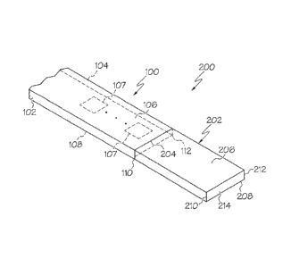
perspective view of an example of an SW waveguide assembly 200 including a
waveguide feed section 202 in accordance with an embodiment of the present
disclosure. The SW waveguide assembly 200 in FIG. 2 may include a waveguide
similar to the SW waveguide 100 in FIGs. 1A-1C.. In the exemplary embodiment
in
FIG 2, the SW waveguide 100 may be terminated by a waveguide feed section 202.
The waveguide feed section 202 may be a rectangular waveguide section 202 as
illustrated in FIG. 2. The waveguide feed section 202 includes a first end 204
that
has a shape and size that corresponds to a shape and size of an end of the SW
waveguide 100 to matingly contact the end of the SW waveguide 100. The
waveguide feed section 202 may be formed by top and bottom conductive walls
206
and 208 and side conductive walls 210 and 212. The top conductive wall 206 of
the
waveguide feed section 202 may correspond to and contact or join the impedance
sheet 106. The bottom conductive wall 208 may correspond to and may contact or
join the base conductive ground plane 108. The side conductive wall 210 may
correspond to and may contact or join the conductive side wall 102 of the
waveguide
100 and the side conductive wall 212 of the waveguide feed section 202 may
correspond to and may contact or join the conductive side wall 112 of the SW
waveguide 100. A waveguide aperture 214 is at an opposite end or second end of
the waveguide feed section 202 from the first end 204 of the waveguide feed
section
202 that interfaces with or joins the SW waveguide 100. The first end 204
defines a
8
CA 02892643 2015-05-20
feed of the waveguide feed section 202 where an electromagnetic wave is
transmitted from the waveguide feed section 202 to the SW waveguide 100. The
waveguide feed section 202 may be connected to standard waveguide feed
components in any of a number of arrangement. For example, the width and
height
of the waveguide feed section 202 may be tapered from the SW waveguide 100
dimensions to the dimensions of a standard waveguide section.
FIG. 3A is a perspective view of an example of an SW waveguide assembly 300
including a waveguide feed section 302 and a coaxial connector 304 integrated
into
the waveguide feed section 302 in accordance with an embodiment of the present
disclosure. FIG. 3B is an end view of the exemplary SW waveguide assembly 300
of FIG. 3A. The SW waveguide assembly 300 in FIG. 3A may include a waveguide
similar to the SW waveguide 100 in FIGs. 1A-1C. In the exemplary embodiment in
FIG 3A, the SW waveguide 100 may be terminated by a waveguide feed section
302. The waveguide feed section 302 may be similar to the waveguide feed
section
202 in FIG. 2. However, the waveguide feed section 302 is terminated by a
conductive end cap 306 rather than an aperture 214. A coaxial feed connector
304
is integrated into the waveguide feed section 302. A center conductor 308 in
the
coaxial connector 304 is used to excite surface waves in the SW waveguide 100
in
response to an electromagnetic signal being transmitted by a coaxial
transmission
line (not shown in FIGs. 3A and 3B) connected to the coaxial connector 304, or
a
surface wave signal may be extracted by the center conductor 308 in response
to an
electromagnetic signal being received by elements 107 of the SW waveguide 100
as
described herein. While the coaxial connector 304 is shown in the exemplary
embodiment in FIGs. 3A and 3B as entering a bottom conductive wall of the
waveguide feed section 302, the coaxial connector 304 may also enter the
waveguide feed section 302 through any of the other walls or through the end
cap
306.
FIG. 4A is a top view of an example of an SW waveguide 400 including a
modulated
impedance sheet 402 and vias 404 (as best shown in FIG. 4B) formed in the
conductive side walls 405 in accordance with an embodiment of the present
9
CA 02892643 2015-05-20
disclosure. Other exemplary embodiments may have only the modulated impedance
sheet 402 or only the vias 404. FIG. 4B is a side view of the exemplary SW
waveguide 400 of FIG. 4A. The SW waveguide 400 may be similar to the SW
waveguide 100 of FIG. 1 except the impedance sheet 106 in FIG. 1 may be
realized
by the impedance sheet 402 that includes an array of conductive patches 406 on
top
of the substrate 114. The conductive side walls 102 and 104 in FIG. 1 may be
replaced by conductive vias 404 that are electrically connected through the
dielectric
substrate 114 from the base conductive ground plane 108 to a metallic strip
408 that
may connect an opposite end or top of the vias 404 to each other on each side
of the
SW waveguide 400 as shown in FIG. 4A. The SW waveguide 400 including the vias
404 may define a substrate integrated waveguide (SIW) with a top conductor
replaced by a patterned metal representing the impedance sheet 402. The
exemplary embodiment in FIGs. 4A and 4B may also be terminated by a waveguide
feed section 410 including an integrated coaxial connector 412 that may be
similar to
the waveguide feed section 302 with integrated coaxial connector 304. The
waveguide assembly 400 could also be terminated by a waveguide feed section
410
similar to waveguide feed section 202 in FIG. 2 or by some other mechanism for
propagating a surface wave in the waveguide assembly 400. The waveguide feed
section 410 may also include conductive vias 414 (best shown in FIG. 4B) that
electrically connect between a bottom wall 416 and an upper wall 418 of the
waveguide feed section 410.
The SW impedance (ZSw) and the corresponding SW index (nsw) for the exemplary
SW waveguides described herein may be determined by the geometric dimensions
of the SW waveguides, the impedance of the impedance sheet (Zsheet), and the
dielectric properties by solving the walled-SW waveguide transverse-resonance
method (TRM) equation ( equation 1) for nsw:
1 nsub 1
__________________________ j
cot (kz,subd)I + ¨ = 0
ko[Zok,0 Zsubkz ,sub Zsheet
where kzo = (1¨ 7/...w) ¨ (5-w)2 and k, ,sub = kg (ns2ub ¨ 441)
(Equation 1)
Where 1(0 is the wavenumber of free-space radiation with the same frequency as
the
surface wave. Zo, Zõb and Zsheet are the impedance of free space, the
dielectric
substrate and the impedance sheet respectively. Nub and d are the refractive
index
and thickness of the dielectric substrate, respectively. w is the width of the
SW
waveguide. When the impedance sheet is realized as an array of conductive
patches, Zsheet is determined from the patch geometry and the substrate
properties.
FIG. 5A is a perspective view of an example of an SW waveguide 500 including
conductive side walls 102 and 104 and a center conductor 506 in accordance
with
an embodiment of the present disclosure. FIG. 5B is an end view of the
exemplary
SW waveguide 500 of FIG. 5A. The SW waveguide 500 may be similar to the SW
waveguide 100 in FIGs. 1A and 1B except including the center conductor 506
embedded within the dielectric substrate 114. The center conductor 506 may
extend
substantially the entire length of the SW waveguide 500 or only partially the
length of
the waveguide 500. The center conductor 506 may have a substantially
rectangular
cross-section as shown in the exemplary embodiment in FIGs. 5A and 5B. In
other
embodiments, the center conductor 506 may have another cross-section, such as
for
example, square, round or some other shape. The center conductor 506 may be
fed
by a coaxial connector 508 shown by broken lines in FIGs. 5A and 5B or by
another
suitable arrangement. The center conductor 506 allows the SW waveguide 500 to
be narrower than other waveguides without a center conductor because the SW
waveguide 500 with the center conductor 506 does not have a low frequency
cutoff.
As previously discussed, narrower SW waveguides can be advantageous for
antenna arrays of SW waveguide AISAs because the waveguides can be spaced
less than about 1/2 A apart. Adjacent SW waveguides may also share a common
side
wall in AISAs.
11
CA 2892643 2017-10-13
CA 02892643 2015-05-20
FIG. 6 is a block schematic diagram of an example of an antenna system 600 in
accordance with an embodiment of the present disclosure. The antenna system
600
may include antenna 602, a voltage controller 604, a phase shifter 606, and a
radio
frequency module 608. The antenna 602 may be an artificial impedance surface
antenna (AISA) 610 in this illustrative example.
The antenna 602 may be configured to transmit and/or a receive radiation
pattern
612. Further, the antenna 602 may be configured to electronically control the
radiation pattern 612, such as the direction of scan or angle of a main lobe
of the
radiation pattern 612. When the antenna 602 is used for transmitting,
radiation
pattern 612 may be the strength of the radio waves transmitted from the
antenna
602 as a function of direction. Radiation pattern 612 may be referred to as a
transmitting pattern when antenna 602 is used for transmitting. When antenna
602
is used for receiving, radiation pattern 612 may be the sensitivity of antenna
602 to
radio waves as a function of direction. Radiation pattern 612 may be referred
to as a
receiving pattern when the antenna 602 is used for receiving. The transmitting
pattern and receiving pattern of antenna 602 may be identical. Consequently,
the
transmitting pattern and receiving pattern of the antenna 602 may be simply
referred
to as radiation pattern 612.
Radiation pattern 612 may include main lobe 616 and one or more side lobes.
Main
lobe 616 may be the lobe at the direction in which antenna 602 is being
directed.
When antenna 602 is used for transmitting, main lobe 616 is located at the
direction
in which antenna 602 transmits the strongest radio waves to form a radio
frequency
beam. When antenna 602 is used for transmitting, main lobe 616 may also be
referred to as the primary gain lobe of radiation pattern 612. When antenna
602 is
used for receiving, main lobe 616 is located at the direction in which antenna
602 is
most sensitive to incoming radio waves.
In this illustrative example, antenna 602 is configured to electronically
steer main
lobe 616 of radiation pattern 612 in a desired direction 614. The main lobe
616 of
radiation pattern 612 may be electronically steered by controlling phi
steering angle
12
CA 02892643 2015-05-20
618 and theta steering angle 620 at which main lobe 616 is directed. Phi
steering
angle 618 and theta steering angle 620 are spherical coordinates. When antenna
602 is operating in an X-Y plane, phi steering angle 618 is the angle of main
lobe
616 in the X-Y plane relative to the X-axis. Further, theta steering angle 620
is the
angle of main lobe 616 relative to a Z-axis that is orthogonal to the X-Y
plane.
Antenna 602 may operate in the X-Y plane by having an array of radiating
elements
622 that lie in the X-Y plane. As used herein, an "array" of items may include
one or
more items arranged in rows and/or columns. In this illustrative example, the
array
of radiating elements 622 may be a single radiating element or a plurality of
radiating
elements. In one illustrative example, each radiating element in the array of
radiating elements 622 may take the form of an artificial impedance surface,
surface
wave waveguide structure. The SW waveguide structure may be similar to one of
those previously described with conductive side walls.
Radiating element 623 may be an example of one radiating element in the array
of
radiating elements 622. Radiating element 623 may be configured to emit
radiation
that contributes to radiation pattern 612.
As depicted, radiating element 623 may be implemented using a dielectric
substrate
624. Radiating element 623 may include one or more surface wave channels that
are formed on the dielectric substrate 624. For example, radiating element 623
may
include a surface wave channel 625. Surface wave channel 625 may be configured
to constrain the path of surface waves propagated along dielectric substrate
624,
and surface wave channel 625 in particular. The surface wave channel 625 may
be
defined by an impedance sheet, such as the impedance sheet 106 disposed on the
dielectric substrate 114 and between the two conductive side walls 102 and 104
in
the exemplary SW waveguide 100 described with reference to FIGs. 1A-1C.
In one illustrative example, the array of radiating elements 622 may be
positioned
substantially parallel to the X-axis and arranged and spaced along the Y-axis.
Further, when more than one surface wave channel is formed on a dielectric
13
CA 02892643 2015-05-20
substrate, these surface wave channels may be formed substantially parallel to
the
X-axis and arranged and spaced along the Y-axis.
In this illustrative example, impedance elements and tunable elements located
on a
dielectric substrate may be used to form each surface wave channel of a
radiating
element in the array of radiating elements 622. For example, surface wave
channel
625 may be comprised of a plurality of impedance elements 626 and a plurality
of
tunable elements 628 located on the surface of the dielectric substrate 624
similar to
that previously described with reference to FIG.1C. Together, the plurality of
impedance elements 626, plurality of tunable elements 628, and dielectric
substrate
624 form an artificial impedance surface from which radiation or
electromagnetic
signals may be transmitted or likewise received by the impedance sheet or SW
channel 625.
An impedance element of the plurality of impedance elements 626 may be
implemented in a number of different ways. In one illustrative example, an
impedance element may be implemented as a resonating element. In one
illustrative example, an impedance element may be implemented as an element
comprised of a conductive material. The conductive material may be, for
example,
without limitation, a metallic material. Depending on the implementation, an
impedance element may be implemented as a metallic strip, a patch of
conductive
paint, a metallic mesh material, a metallic film, a deposit of a metallic
substrate, or
some other type of conductive element. In some cases, an impedance element may
be implemented as a resonant structure such as, for example, a split-ring
resonator
(SRR), an electrically-coupled resonator (ECR), a structure comprised of one
or
more metamaterials, or some other type of structure or element.
Each one of plurality of tunable elements 628 may be an element that can be
controlled, or tuned, to change an angle of the one or more surface waves
being
propagated along radiating element 623. In this illustrative example, each of
the
plurality of tunable elements 628 may be an element having a capacitance that
can
be varied based on the voltage applied to the tunable element.
14
CA 02892643 2015-05-20
In one illustrative example, a plurality of impedance elements 626 may take
the form
of a plurality of metallic strips 632 and a plurality of tunable elements 628
may take
the form of a plurality of varactors 634. Each of plurality of varactors 634
may be a
semiconductor element diode that has a capacitance dependent on the voltage
applied to the semiconductor element diode.
In one illustrative example, the plurality of metallic strips 632 may be
arranged in a
row that extends along the X-axis. For example, the plurality of metallic
strips 132
may be periodically distributed on the dielectric substrate 624 along the X-
axis. The
plurality of varactors 634 may be electrically connected to the plurality of
metallic
strips 632 on the surface of dielectric substrate 624. In particular, at least
one
varactor of the plurality of varactors 634 may be positioned between each
adjacent
pair of metallic strips of the plurality of metallic strips 632. Further, the
plurality of
varactors 634 may be aligned such that all of the varactor connections on each
metallic strip have the same polarity.
The dielectric substrate 624, plurality of impedance elements 626, and
plurality of
tunable elements 628 may be configured with respect to a selected design
configuration 636 for the surface wave channel 625, and radiating element 623
in
particular. Depending on the implementation, each radiating element in the
array of
radiating elements 622 may have a same or different selected design
configuration.
As depicted, selected design configuration 636 may include a number of design
parameters such as, but not limited to, impedance element width 638, impedance
element spacing 640, tunable element spacing 642, and substrate thickness 644.
Impedance element width 638 may be the width of an impedance element in the
plurality of impedance elements 626. Impedance element width 638 may be
selected to be the same or different for each of plurality of impedance
elements 626,
depending on the implementation.
Impedance element spacing 640 may be the spacing of the plurality of impedance
elements 626 with respect to the X-axis. Tunable element spacing 642 may be
the
spacing of the plurality of tunable elements 628 with respect to the X-axis.
Further,
CA 02892643 2015-05-20
substrate thickness 644 may be the thickness of the dielectric substrate 624
on
which a particular waveguide is implemented.
The values for the different parameters in the selected design configuration
636 may
be selected based on, for example, without limitation, the radiation frequency
at
which antenna 602 is configured to operate. Other considerations include, for
example, the desired impedance modulations for antenna 602.
Voltages may be applied to the plurality of tunable elements 628 by applying
voltages to the plurality of impedance elements 626 because the plurality of
impedance elements 626 may be electrically connected to the plurality of
tunable
elements 628. In particular, the voltages applied to the plurality of
impedance
elements 626, and thereby the plurality of tunable elements 628, may change
the
capacitance of the plurality of tunable elements 628. Changing the capacitance
of
the plurality of tunable elements 628 may, in turn, change the surface
impedance of
the antenna 602. Changing the surface impedance of the antenna 602 changes the
radiation pattern 612 produced.
In other words, by controlling the voltages applied to the plurality of
impedance
elements 626, the capacitances of the plurality of tunable elements 628 may be
varied. Varying the capacitances of the plurality of tunable elements 628 may
vary,
or modulate, the capacitive coupling and impedance between the plurality of
impedance elements 626. Varying, or modulating, the capacitive coupling and
impedance between the plurality of impedance elements 626 may change the theta
steering angle 620 of the antenna 602.
The voltages may be applied to the plurality of impedance elements 626 using
voltage controller 604. Voltage controller 604 may include a number of voltage
sources 646, number of grounds 648, number of voltage lines 650, and/or some
other type of component. In some cases, voltage controller 604 may be referred
to
as a voltage control network.
16
CA 02892643 2015-05-20
A voltage source in the number of voltage sources 646 may take the form of,
for
example, without limitation, a digital to analog converter (DAC), a variable
voltage
source, or some other type of voltage source. The grounds 648 may be used to
ground at least a portion of the plurality of impedance elements 626. The
voltage
lines 650 may be used to transmit voltage from the respective voltage sources
646
and/or grounds 648 to the plurality of impedance elements 626.
In one illustrative example, each of the plurality of impedance elements 626
may
receive voltage from one of the number of voltage sources 646. In another
illustrative example, a portion of the plurality of impedance elements 626 may
receive voltage from the number of voltage sources 646 through a corresponding
portion of the number of voltage lines 650, while another portion of the
plurality of
impedance elements 626 may be electrically connected to respective ones of the
number of grounds 648 through a corresponding portion of the number of voltage
lines 650.
In some cases, the controller 651 may be used to control the number of voltage
sources 646. Controller 651 may be considered part of or separate from antenna
system 600, depending on the implementation. Controller 651 may be implemented
using a microprocessor, an integrated circuit, a computer, a central
processing unit,
a plurality of computers in communication with each other, or some other type
of
computer or processor.
Surface waves 652 propagated along the array of radiating elements 622 may be
coupled to a number of transmission lines 656 by a plurality of surface wave
feeds
630 located on the dielectric substrate 624. A surface wave feed of the
plurality of
surface wave feeds 630 may be any device that is capable of converting a
surface
wave into a radio frequency signal and/or a radio frequency signal into a
surface
wave. In one illustrative example, a surface wave feed of the plurality of
surface
wave feeds 630 is located at the end of each waveguide in the array of
radiating
elements 622 on dielectric substrate 624. Similar to that previously
described, the
17
CA 02892643 2015-05-20
surface wave feeds 630 may be a waveguide feed section similar to waveguide
feed
sections 202 and 302 in FIGs. 2 and 3A respectively.
For example, when antenna 602 is in a receiving mode, the one or more surface
waves propagating along radiating element 623 may be received at a
corresponding
surface wave feed of the plurality of surface wave feeds 630 and converted
into a
corresponding radio frequency signal 654. Radio frequency signal 654 may be
sent
to the radio frequency module 608 over one or more transmission lines 656.
Radio
frequency module 608 may then function as a receiver and process radio
frequency
signal 654 accordingly.
Depending on the implementation, radio frequency module 608 may function as a
transmitter, a receiver, or a combination of the two. In some illustrative
examples,
radio frequency module 608 may be referred to as transmit/receive module 658
or
transceiver.
In some cases, radio frequency signal 654 may pass through the phase shifter
606
prior to being sent to radio frequency module 608. Phase shifter 606 may
include
any number of phase shifters, power dividers, transmission lines, and/or other
components configured to shift the phase of radio frequency signal 654. In
some
cases, phase shifter 606 may be referred to as a phase-shifting network.
When antenna 602 is in a transmitting mode, radio frequency signal 654 may be
sent from radio frequency module 608 to antenna 602 over the transmission
lines
156. In particular, radio frequency signal 654 may be received at one of the
plurality
of surface wave feeds 630 and converted into one or more surface waves that
are
then propagated along a corresponding waveguide in the array of radiating
elements
622.
In this illustrative example, the relative phase difference between the
plurality of
surface wave feeds 630 may be changed to change a phi steering angle 618 of
the
radiation pattern 612 that is transmitted or received. Thus, by controlling
the relative
phase difference between the plurality of surface wave feeds 630 and
controlling the
18
CA 02892643 2015-05-20
voltages applied to the tunable elements of each waveguide in array of
radiating
elements 622, the phi steering angle 618 and theta steering angle 620,
respectively,
may be controlled. In other words, antenna 602 may be electronically steered
in two
dimensions. The phi steering angle may be defined as controlling the angular
direction of a main beam of the radiation pattern of the antenna 602 in a
plane
corresponding to the plane of the antenna 602 or in an X-Y coordinate plane.
The
theta steering angle may be defined as controlling the angular direction of
the main
beam of the radiation pattern in a direction perpendicular to the plane of the
antenna
602 or in an X-Z coordinate plane.
Depending on the implementation, radiating element 623 may be configured to
emit
linearly polarized radiation or circularly polarized radiation. When
configured to emit
linearly polarized radiation, the plurality of metallic strips used for each
surface wave
channel on radiating element 623 may be angled in the same direction relative
to the
X-axis along which the plurality of metallic strips are distributed.
Typically, only a
single surface wave channel is needed for each radiating element 623.
However, when radiating element 623 is configured for producing circularly
polarized
radiation, surface wave channel 625 may be a first surface wave channel and a
second surface wave channel 645 may also be present in radiating element 623.
Surface wave channel 625 and second surface wave channel 645 may be about 90
degrees out of phase from each other. The interaction between the radiation
from
these two coupled surface wave channels makes it possible to create circularly
polarized radiation.
The plurality of impedance elements 626 that form surface wave channel 625 may
be a first plurality of impedance elements that radiate with a polarization at
an angle
to the polarization of the surface wave electric field. A second plurality of
impedance
elements that form a second surface wave channel 645 may radiate with a
polarization at an angle offset about 90 degrees as compared to surface wave
channel 625.
19
CA 02892643 2015-05-20
For example, each impedance element in the first plurality of impedance
elements of
surface wave channel 625 may have a tensor impedance with a principal angle
that
is angled at a first angle relative to an X-axis of radiating element 623.
Further, each
impedance element in the second plurality of impedance elements of the second
surface wave channel 645 may have a tensor impedance that is angled at a
second
angle relative to the X-axis of the corresponding radiating element. The
difference
between the first angle and the second angle may be about 90 degrees.
The capacitance between the first plurality of impedance elements may be
controlled
using plurality of tunable elements 628, which may be a first plurality of
tunable
elements. The capacitance between the second plurality of impedance elements
may be controlled using a second plurality of tunable elements.
As a more specific example, the plurality of metallic strips 632 on surface
wave
channel 625 may be angled at about positive 45 degrees with respect to the X-
axis
along which plurality of metallic strips 632 is distributed. However, the
plurality of
metallic strips used for second surface wave channel 645 may be angled at
about
negative 45 degrees with respect to the X-axis along which the plurality of
metallic
strips is distributed. This variation in tilt angle produces radiation of
different linear
polarizations, that when combined with a 90 degree phase shift, may produce
circularly polarized radiation.
The illustration of antenna system 600 in Figure 1 is not meant to imply
physical or
architectural limitations to the manner in which an illustrative embodiment
may be
implemented. Other components in addition to or in place of the ones
illustrated
may be used. Some components may be optional. Also, the blocks are presented
to
illustrate some functional components. One or more of these blocks may be
combined, divided, or combined and divided into different blocks when
implemented
in an illustrative embodiment.
For example, in other illustrative examples, phase shifter 606 may not be
included in
antenna system 600. Instead, the transmission lines 656 may be used to couple
the
plurality of surface wave feeds 630 to a number of power dividers and/or other
types
CA 02892643 2015-05-20
of components, and these different components to radio frequency module 608.
In
some examples, the transmission lines 656 may directly couple the plurality of
surface wave feeds 630 to the radio frequency module 608.
In some illustrative examples, a tunable element of the plurality of tunable
elements
628 may be implemented as a pocket of variable material embedded in dielectric
substrate 124. As used herein, a "variable material" may be any material
having a
permittivity that may be varied. The permittivity of the variable material may
be
varied to change, for example, the capacitance between two impedance elements
between which the variable material is located. The variable material may be a
voltage-variable material or any electrically variable material, such as, for
example,
without limitation, a liquid crystal material or barium strontium titanate
(BST).
In other illustrative examples, a tunable element of the plurality of tunable
elements
628 may be part of a corresponding impedance element of the plurality of
impedance elements 626. For example, a resonant structure having a tunable
element may be used. The resonant structure may be, for example, without
limitation, a split-ring resonator, an electrically-coupled resonator, or some
other type
of resonant structure.
FIG. 7 is a schematic diagram of an example of an antenna system 700 including
an
array of SW waveguides 702a-702n with conductive side walls 704 in accordance
with an embodiment of the present disclosure. The antenna system 700 may be
used for the antenna system 600 of FIG. 6. The array of SW waveguides 702a-
702n
may form an AISA 706. The SW waveguides 702a-702n may be similar to any of
the SW waveguides with conductive side walls described herein or other SW
waveguide assembly that include conductive side walls. Accordingly, the SW
waveguides 702a-702n may be similar to the SW waveguide 100 described with
reference to FIGs. 1A-1C, SW waveguide 200 in FIG. 2, SW waveguide 300 in FIG.
3A, SW waveguide 400 in FIGs. 4A-4B, SW waveguide 500 in FIGs. 5A-5B or other
SW waveguide including conductive side walls similar to that described herein.
As
depicted in FIG. 7, the adjacent SW waveguides 702a-702n may share a common
21
CA 02892643 2015-05-20
side wall 704 that permits the adjacent SW waveguides 702a-702n to be spaced
less than about 1/2 A apart in an array of SW AISAs. In another embodiment,
the side
walls 704 of adjacent SW waveguides 702a-704n may abut one another rather than
share a common side wall.
In the exemplary embodiment illustrated in FIG. 7, the SW waveguides 702a-704n
may each include a impedance sheet 708 similar to the impedance sheet 106
described with reference to FIG. 1C. However, other impedance sheets similar
to
those described herein or other configurations may also be used depending upon
the particular performance and radiation pattern characteristics desired. In
the
exemplary embodiment of FIG. 7, the impedance sheet 708 may include a
plurality
of metallic patches 710. The metallic patches 710 may also be referred to as
radiating elements. The metallic patches 710 may be spaced from one another at
a
uniform distance or may be spaced according to a particular pattern, such as
alternating wide and narrow spacing. The metallic patches 710 may also be the
same width or may have different widths, such as for example alternating wide
and
narrow widths. At least one tunable element 712 or variable reactive element
may
be electrically connected between adjacent metallic patches 710. Examples of
the
tunable element 712 or variable reactive element may include, but is not
necessarily
limited to a varactor, a liquid crystal element, a tunable material element
comprising
barium strontium nitrate or other tunable impedance element capable of
modulating
or tuning the impedance sheet 708 to provide certain performance
characteristics,
such as those described herein, for example, steering a main lobe or beam of a
radiation pattern of the SW AISA 706. As described in more detail herein the
tunable element 712 may be configured to be tuned by a voltage being connected
to
at least one of the adjacent metallic patches 710 or by electric field or
magnetic field
being coupled to the tunable element 712.
The antenna system 700 may also include a controller 714 and voltage
controller
716 configured to control a voltage or voltages applied to the tunable
elements 712
and/or metallic patches 710 for controlling operation and steering of the SW
AISA
706. The controller 714 may be similar to the controller 651 described with
22
CA 02892643 2015-05-20
reference to FIG. 6 and the voltage controller 716 may be similar to voltage
controller 604. The voltage controller 716 may include a digital-to-analog
converter
718.
The antenna system 700 may also include a radio frequency (RF) transceiver 720
that may be coupled to the SW AISA 706 by a plurality of transmission lines
722 and
a phase shifter 724. The RF transceiver 720 may be similar to the RF module
608 of
FIG. 6 and the phase shifter 724 may be similar to the phase shifter 606 in
FIG. 6.
The RF transceiver 720 may transmit and receive electromagnetic or RF signals
to
and from the SW AISA 706 via the transmission lines 722 and phase shifter 724
similar to that described with respect to the exemplary embodiment of FIG. 6.
FIG. 8 is an example of a method 800 of operation of an antenna system
including
SW waveguides with conductive sides in accordance with an embodiment of the
present disclosure. The method 800 may be embodied in and performed by the
system 600 of FIG. 6 or 700 of FIG. 7. In block 802, an electromagnetic signal
may
be transmitted along an SW waveguide of an AISA array. The SW waveguide may
include a tunable impedance sheet disposed between conductive side walls
similar
to that described herein. The tunable impedance sheet may include a plurality
of
electromagnetic radiating elements and tunable elements associated with the
radiating elements.
In block 804, a radiation pattern may be generated by the SW AISA in response
to
the electromagnetic signal.
In block 806, the tunable elements of the impedance sheet may be
electronically
tuned to scan or steer a main radiation lobe of the radiation pattern over a
range of
angles in a direction perpendicular to a plane of the antenna (theta
direction). A
control voltage may be applied to the tunable element associated with each
radiating
element to scan or steer the antenna.
23
CA 02892643 2015-05-20
In block 808, the main lobe may be electronically steered in a plane of the SW
AISA
(phi direction) by controlling a relative phase difference between a plurality
of SW
feeds of the SW AISA.
The flowchart and block diagrams in the Figures illustrate the architecture,
functionality, and operation of possible implementations of systems, methods,
and
computer program products according to various embodiments of the present
disclosure. In this regard, each block in the flowchart or block diagrams may
represent a module, segment, or portion of instructions, which comprises one
or
more executable instructions for implementing the specified logical
function(s). In
some alternative implementations, the functions noted in the block may occur
out of
the order noted in the figures. For example, two blocks shown in succession
may, in
fact, be executed substantially concurrently, or the blocks may sometimes be
executed in the reverse order, depending upon the functionality involved. It
will also
be noted that each block of the block diagrams and/or flowchart illustration,
and
combinations of blocks in the block diagrams and/or flowchart illustration,
can be
implemented by special purpose hardware-based systems that perform the
specified
functions or acts or carry out combinations of special purpose hardware and
computer instructions.
The terminology used herein is for the purpose of describing particular
embodiments
only and is not intended to be limiting of any embodiments. As used herein,
the
singular forms "a", "an" and "the" are intended to include the plural forms as
well,
unless the context clearly indicates otherwise. It will be further understood
that the
terms "comprises" and/or "comprising," when used in this specification,
specify the
presence of stated features, integers, steps, operations, elements, and/or
components, but do not preclude the presence or addition of one or more other
features, integers, steps, operations, elements, components, and/or groups
thereof.
The corresponding structures, materials, acts, and equivalents of all means or
step
plus function elements in the claims below are intended to include any
structure,
material, or act for performing the function in combination with other claimed
24
CA 02892643 2015-05-20
elements as specifically claimed. The description herein has been presented
for
purposes of illustration and description, but is not intended to be exhaustive
or
limited to embodiments in the form disclosed. Many modifications and
variations will
be apparent to those of ordinary skill in the art without departing from the
intent of
the embodiments of the described. The embodiments were chosen and described in
order to best explain certain principles of practical application, and to
enable others
of ordinary skill in the art to understand that various embodiments with
various
modifications can be adapted to the particular use contemplated.
Although specific embodiments have been illustrated and described herein,
those of
ordinary skill in the art will appreciate that any arrangement which is
calculated to
achieve the same purpose may be substituted for the specific embodiments shown
and that some embodiments may have other applications in other environments.
This application is intended to cover any adaptations or variations of the
embodiments described. The following claims are in no way intended to be
limited
to the specific embodiments described herein.