Note: Descriptions are shown in the official language in which they were submitted.
CA 02892779 2015-05-22
T054 P02804-US
ELECTRONIC DEVICE SOCKET
Field
[01] The following relates generally to an electronic device mount, and
more particularly
to an electronic device socket especially suited for mounting a pluggable
electronic device
on a printed circuit board.
Background
[02] In the computer chip industry, there are several methods used to mount
an
electronic device, such as a semiconductor device, to a printed circuit board.
One such
method is by mounting the electronic device in a device socket which is
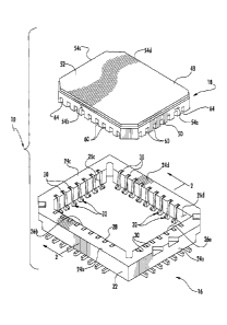
soldered onto the
printed circuit board. Pursuant to the teachings of this method, the socket
includes a
plurality of contact members which are resiliently engageable with the
electronic device.
More particularly, the electronic device has a plurality of spaced-apart
receiving slots
(castellations) aligned with the contact members of the device socket for
receiving the
contact members therein. Each of the contact members resiliently engages the
device for
securing the electronic device to the device socket and for providing
electrical continuity
between the electronic device, device socket and printed circuit board.
[03] One disadvantage associated with this method is that the electronic
device may
"pop-out" of the device socket if it is not physically restrained with
sufficient contact spring
force, a clip or other retention mechanism. This is particularly true for
electronic devices
that are substantially heavy. The weight and the center of mass of an
electronic device can
1
CA 02892779 2015-05-22
T054 P02804-US
cause it to fall out of the device socket, particularly when mounted in a
vertical or inverted
orientation. In addition, vibration and thermal cycling can also cause gradual
loosening of
the devices from the socket contacts. Accordingly, there is presently a need
for a mounting
system which more securely retains an electronic device to a printed circuit
board without
the need for external retention clips.
Summary
[04] In one embodiment, there is provided: an electronic device mounting
system which
may improve the electrical contact between the electronic device and the
device socket;
the provision of such a mounting system which may provide increased frictional
contact
between the device socket and the electronic device; the provision of such a
mounting
system which may make it easy to replace an electronic device on a printed
circuit board;
and the provision of such a mounting system which may be easy to install.
[05] In general, the electronic device socket of one embodiment is mounted
(e.g., by
soldering) on a printed circuit board. The socket has a frame with inwardly
facing surfaces
which define an opening, and a plurality of spaced-apart, inwardly projecting
contact
members each being mounted on the frame and resiliently movable along a plane
generally
perpendicular to the plane of its respective surface. Each contact member is
constructed of
electrically conductive material and has an inwardly extending contact point.
The socket is
configured and arranged to receive an electronic device, such as a
semiconductor device.
The electronic device has outwardly facing surfaces adapted to face the
inwardly facing
surfaces of the device socket when placing the device within the opening of
the socket, and
2
CA 02892779 2015-05-22
=
T054 P02804-US
a plurality of spaced-apart receiving slots in registry with and capable of
receiving the
contact members therein for securing the device to the socket. Each receiving
slot has an
electrically conductive surface mount for providing electrical connection
between the
device, device socket and printed circuit board when the contact point of each
contact
member is in resilient engagement with the electrically conductive surface
mount of its
respective receiving slot.
[06] The socket can be provided to a user without a device mounted thereto.
This allows
a user to mount an electronic device onto a printed circuit board to which the
socket is
secured. Alternatively, the socket can be provided to a user with a device
mounted thereto.
The socket and device can be incorporated in a fully formed electronic device.
[07] To allow the electronic device socket to support heavier devices, the
contact
member may have a textured surface on its contact point. Preferably, the
textured surface
is a serrated surface. The textured surface or serrations increase the
frictional engagement
of the contact member with the device mounted in the socket. The textured
surface or
serrations may be cut into or superposed on a rounded surface of the contact
point.
[08] In one embodiment, each individual contact point has a textured
surface or
serrations. In other embodiments, selective location of the serrated contact
points allows
the manufacturer to adjust and optimize insertion and removal force for the
socket. For
example, in one embodiment, a textured surface or serrations are provided on
alternating
contact points. In yet another embodiment, a textured surface or serrations
are provided
3
CA 02892779 2015-05-22
=
' T054 P02804-US
,
,
only on contact points that engage the corner surface contacts of the
electronic device.
Other configurations are also possible.
[09] According to one embodiment, there is provided a socket capable of
mounting an
electronic device on a printed circuit board, the electronic device having
outwardly facing
surfaces and a plurality of spaced-apart receiving slots, each receiving slot
having an
electrically conductive surface mount, said socket comprising: a frame with
inwardly facing
surfaces which define an opening, said inwardly facing surfaces being adapted
to face the
outwardly facing surfaces of the electronic device when placing the electronic
device within
the opening of the socket; a plurality of spaced-apart, inwardly projecting
contact members
each being mounted on the frame and resiliently movable along a plane
generally
perpendicular to the plane of its respective surface, each contact member
being
constructed of electrically conductive material and having a leg with a base
and an inwardly
extending, tapered contact point; wherein said contact members are in registry
with and
capable of being received in the spaced-apart receiving slots on the device
for securing the
electronic device to the socket and for providing electrical connection
between the
electronic device, socket, and a printed circuit board when said contact point
of each
contact member is in resilient engagement with the electrically conductive
surface mount of
its respective receiving slot; wherein said contact point of each contact
member is formed
to taper from the base of the leg in a widthwise dimension to a narrowed end
for enhancing
the electrical connection between said contact member and surface mount; and
wherein,
on at least one of said contact members, said contact point has a textured
surface for
4
CA 02892779 2015-05-22
T054 P02804-US
increasing frictional engagement between said contact member and said
electronic device
thereby maintaining said electronic device and socket in assembled relation.
In some
embodiments, the textured surface of said contact point of said at least one
contact
member is a serrated surface, said serrated surface having at least one peak
extending
inwardly to engage the electronic device received in said opening. In some
embodiments,
the serrated surface of said contact point is defined by notches defined on a
rounded
surface. In some embodiments, the electrically conductive surface mount of
each receiving
slot is flat or concave. In some embodiments, on each of said contact members,
said contact
,
point has a serrated surface for increasing frictional engagement between said
contact
member and said electronic device thereby maintaining said electronic device
and socket in
assembled relation. In some embodiments, on alternating contact members, said
contact
point has a serrated surface for increasing frictional engagement between said
contact
member and said electronic device thereby maintaining said electronic device
and socket in
assembled relation, and wherein on each contact member between said
alternating contact
members, said contact point does not have a serrated surface. In some
embodiments, on
contact members adjacent to corners of the frame, said contact point has a
serrated surface
for increasing frictional engagement between said contact member and said
electronic
device thereby maintaining said electronic device and socket in assembled
relation, and
wherein on each of the other contact members, said contact point does not have
a serrated
surface.
CA 02892779 2015-05-22
1054 P02804-US
110] According to another embodiment, there is provided an electrically
conductive
contact member for an electronic device socket comprising: a base portion; an
inverted U-
shaped leg portion extending from the base, said leg portion having a terminal
end, said
terminal end being resiliently movable; and an inwardly extending, tapered
contact point on
said terminal end of said leg portion, said contact point tapering from the
terminal end of
the leg portion in a widthwise dimensions to a narrowed end, said contact
point having a
plurality of contact serrations for increasing frictional engagement with a
corresponding
surface contact.
[11] According to another embodiment, there is provided a socket
capable of mounting
an electronic device on a printed circuit board, the electronic device having
outwardly
facing surfaces and a plurality of spaced-apart receiving slots adjacent to a
bottom of the
device, each receiving slot having a vertically oriented electrically
conductive contact
surface, said socket comprising: a frame with inwardly facing surfaces which
define an
opening, said inwardly facing surfaces being adapted to face the outwardly
facing surfaces
of the electronic device when placing the electronic device within the opening
of the socket;
a plurality of spaced-apart, inwardly projecting contact members each being
mounted on
the frame, each contact member having a base portion, and an inverted U-shaped
leg
portion extending from the base, the leg portion having a terminal end which
is resiliently
movable along a plane generally perpendicular to a plane extending along a
respective
inwardly facing surface of said frame, each contact member being constructed
of
electrically conductive material, said terminal end having an inwardly
extending, tapered
6
CA 02892779 2015-05-22
,
T054 P02804-US
contact point; wherein said contact members are in registry with and capable
of being
received in the spaced-apart receiving slots on the device for securing the
electronic device
to the socket and for providing electrical connection between the electronic
device, socket,
and the printed circuit board when said contact point of each contact member
is in resilient
engagement with the electrically conductive contact surface of its respective
receiving slot;
wherein said contact point of each contact member is formed to taper from the
base of the
leg in a widthwise dimension to a narrowed end for enhancing the electrical
and physical
connection between said contact member and said contact surface; and wherein,
on at
least one of said contact members, said contact point has a textured surface
for increasing
sliding frictional engagement between said contact member and said contact
surface of said
electronic device thereby maintaining said electronic device and socket in
assembled
relation; wherein said textured surface of said contact point of said at least
one contact
member is a serrated tooth surface, said serrated tooth surface having at
least two distinct
horizontally extending teeth extending inwardly, each of the teeth having an
angled peak
with a vertex which frictionally engages and bites into said contact surface,
said biting
frictional engagement enhancing electrical and physical contact therebetween
and reducing
perpendicular sliding movement of said contact surface relative to said
serrated tooth
surface. In some embodiments, said serrated surface of said contact point is
defined by
notches defined on a rounded surface. In some embodiments, said socket is
capable of
mounting an electronic device having outwardly facing surfaces and a plurality
of spaced-
apart receiving slots, each receiving slot having an electrically conductive
surface mount,
7
CA 02892779 2015-05-22
1054 P02804-US
said electrically conductive surface mount of each receiving slot being flat
or concave. In
some embodiments, on alternating contact members, said contact point has a
serrated
surface for increasing frictional engagement between said contact member and
said
electronic device thereby maintaining said electronic device and socket in
assembled
relation, and wherein on each contact member between said alternating contact
members,
said contact point does not have a serrated surface. In some embodiments, said
plurality of
contact members comprises contact members adjacent to corners of the frame and
contact
members in middle portions of the frame, wherein, on contact members adjacent
to
corners of the frame, said contact point has a serrated surface for increasing
frictional
engagement between said contact member and said electronic device thereby
maintaining
said electronic device and socket in assembled relation, and wherein on
contact members in
middle portions of the frame, said contact point does not have a serrated
surface.
[12] According to another embodiment, there is provided an electrically
conductive
contact member for an electronic device socket comprising: a base portion; an
inverted U-
shaped leg portion extending from the base, said leg portion having a terminal
end, said
terminal end being resiliently movable; and an inwardly extending, tapered
contact point on
said terminal end of said leg portion, said contact point tapering from the
terminal end of
the leg portion in a widthwise dimensions to a narrowed end, said contact
point having a
plurality of contact serrations for increasing sliding frictional engagement
with a
corresponding surface contact, said contact serrations further comprising at
least two
distinct horizontally extending serrated teeth extending inwardly, each of the
teeth having
8
CA 02892779 2015-05-22
T054 P02804-US
an angled peak with a vertex which frictionally engages and bites into a
contact surface of
said electrically conductive surface mount, said biting frictional engagement
enhancing
electrical and physical contact therebetween and reducing perpendicular
sliding movement
of said contact surface relative to said serrated tooth surface.
[13] According to another embodiment, there is provided a socket capable
of mounting
an electronic device on a printed circuit board, the electronic device having
outwardly
facing surfaces and a plurality of spaced-apart concave receiving slots
adjacent to a bottom
of the device, each concave receiving slot having a vertically oriented
electrically conductive
concave contact surface, said socket comprising: a frame with inwardly facing
surfaces
which define an opening, said inwardly facing surfaces being adapted to face
the outwardly
facing surfaces of the electronic device when placing the electronic device
within the
opening of the socket; a plurality of spaced-apart, inwardly projecting
contact members
each being mounted on the frame, each contact member having a base portion,
and an
inverted U-shaped leg portion extending from the base, the leg portion having
a terminal
end which is resiliently movable along a plane generally perpendicular to a
plane extending
along a respective inwardly facing surface of said frame, each contact member
being
constructed of electrically conductive material, said terminal end having an
inwardly
extending, tapered contact point; wherein said contact members are in registry
with and
capable of being received in the spaced-apart concave receiving slots on the
device for
securing the electronic device to the socket and for providing electrical
connection between
the electronic device, socket, and the printed circuit board when said contact
point of each
9
CA 02892779 2015-05-22
T054 P02804-US
contact member is in resilient engagement with the electrically conductive,
concave contact
surface of its respective receiving slot; wherein said contact point of each
contact member
is formed to taper from the base of the leg in a widthwise dimension to a
narrowed end for
enhancing the electrical and physical connection between said contact member
and said
concave contact surface; and wherein, on at least one of said contact members,
said
contact point has a textured surface for increasing sliding frictional
engagement between
said contact member and said contact surface thereby maintaining said
electronic device
and socket in assembled relation; wherein said textured surface of said
contact point of said
at least one contact member is a serrated tooth surface, said serrated tooth
surface having
at least two distinct horizontally extending teeth extending inwardly, each of
the teeth
having an angled peak with a vertex which frictionally engages and bites into
said concave
contact surface, said biting frictional engagement enhancing electrical and
physical contact
therebetween and reducing perpendicular sliding movement of said concave
contact
surface relative to said serrated tooth surface.
[14] Other objects, features and advantages of certain embodiments shall
become apparent as
the description thereof proceeds when considered in connection with the
accompanying
illustrative drawings.
Description of the Drawings
[15] In the drawings:
[16] Fig. 1 is an exploded perspective view of the socket and an electronic
device;
CA 02892779 2015-05-22
1054 P02804-US
[17] FIG. 2 is a cross-sectional view of the device socket taken along line
2-2 of FIG. 1;
[18] FIG. 3 is an enlarged perspective view of a contact member of the
socket;
[19] Fig. 4 is a cross-sectional view of a larger electronic device mounted
in the device
socket;
[20] Fig. 5 is a magnified view of the contact area encircled in Fig. 4;
[21] Fig. 6 is a further magnified view of the serrated contact point
encircled in Fig. 5;
[22] Fig. 7 is a perspective view of another exemplary embodiment having
contact
members that alternate between serrated contact points and non-serrated
contact points
along one side of the frame opening; and
[23] Fig. 8 is a perspective view of still another exemplary embodiment
having serrated
contact points towards the corners of the socket frame.
[24] Description of the Preferred Embodiments:
[25] Referring now to the drawings, the electronic device socket system of
one
embodiment is illustrated and generally indicated at 10 in Figs. 1-6. The
socket system 10
includes a socket 16 which is capable of mounting an electronic device 18 on a
printed
circuit board (not shown). The electronic device 18 may be a semiconductor
device, other
computer device, a vision device, or any another pluggable electronic device.
As will
hereinafter be more fully described, the instant electronic device socket 16
provides both
electrical and frictional engagement between the device socket 16 and the
device 18.
11
CA 02892779 2015-05-22
1054 P02804-US
[26] Referring to FIG. 1, the electronic device socket 16 comprises a
rectangular (or
square) frame 22 fabricated from insulating (nonconductive) material, such as
plastic or
ceramic material. The frame 22 has four rail members 24a, 24b, 24c and 24d
having
respective inwardly facing surfaces 26a, 26b, 26c and 26d which together
define a
rectangular (or square) opening 28. It should be noted that while the socket
16 is illustrated
as comprising a rectangular or square configuration, any one of a variety of
socket shapes is
contemplated. For example, the socket 16 could easily comprise a circular,
octagonal or
other shape suitable for receiving standard or custom shaped electronic
devices 18.
[27] Turning back to Figs. 1 and 2, a plurality of vertically disposed,
relatively thin,
notches 30 are formed in the inwardly facing surfaces 26a-26d of the frame 22.
Each notch
30 receives an inwardly projecting contact member generally indicated at 32
suitably
mounted on the frame 22 and resiliently moveable along a plane generally
perpendicular to
the plane of its respective surface 26a-26d. As illustrated throughout the
drawings, there
are provided a plurality (e.g., nine) contact members 32 on the long rail
members 24b, 24d
of the frame 22 and a plurality (e.g., seven) contact members 32 on the short
rail members
24a, 24c of the frame 22. It should be understood that any number of contact
members 32
may be provided and fall within the scope of the present invention. Each
contact member
32 is constructed of electrically conductive material, such as beryllium
copper or any
conductive material which is gold plated, non-plated, or with any type of
plating.
[28] FIGS. 2 and 3 better illustrate the attachment of the contact members
32 to the
frame 22 of the device socket 16 and the construction of each contact member
32. As
12
CA 02892779 2015-05-22
T054 P02804-US
illustrated in FIG. 2, there are vertically oriented cavities 34 formed in the
underside of the
frame 22 which receive upwardly extending extensions 36 of the contact members
32 for
attaching the contact members 32 to the frame 22. More specifically, for each
contact
member 32, the extension 36 is formed with a tapered head 38 which has an
interference
fit with the frame 22 when inserting the head 38 of the extension into the
bore 34.
Referring to FIG. 3, each contact member 32 also includes an inverted U-shaped
contact
spring 40 wherein an inner leg 42 of the contact spring 40 is disposed within
the notch 30 of
the frame 22 for providing lateral stability to the contact member 32 and an
outer leg 44 of
the portion which extends inwardly within the opening 28 of the frame 22. The
outer leg 44
is resiliently attached to the inner leg 42 so that it can resiliently move
along the
aforementioned plane in a generally perpendicular direction with respect to
the plane of its
respective surface 26a-26d. Each outer leg 44 has a tapered contact point 46
which is best
illustrated in Figs. 3 and 6. The contact point 46 ensures that electrical
connection is made
between the contact member 32 and the device 18. More specifically, the
contact point 46
is formed to taper from the base of the leg 44 in a widthwise dimension to a
narrowed,
rounded end. Additionally, the tapered contact point 46 is provided with
textured, i.e.
serrated formations 46a that significantly improve the frictional engagement
of the contact
point 46 with the device 18. The importance of this particular construction
will become
apparent as the description of the mounting socket 16 continues.
[29] Turning back to FIG. 1, the electronic device 18 comprises a
rectangular (or square)
frame 48 having a rectangular base portion 50 and a top wall 52 which overlies
the base
13
CA 02892779 2015-05-22
T054 P02804-US
portion 50. Like the frame 22 of the device socket 16, the electronic device
frame 48 is
fabricated from insulating (nonconductive) material, such as plastic or
ceramic material. The
base portion 50 has four outwardly facing surfaces 54a, 54b, 54c and 54d which
are adapted
to face the inwardly facing surfaces 26a-26d of the device socket 16 when
placing the
device 18 within the opening 28 of the socket 16.
[30] As best illustrated in FIG. 1, the base portion 50 of the
electronic device 18 has a
plurality of spaced-apart receiving slots 60 (castellations) in registry with
and capable of
receiving the contact members 32 therein when the device 18 is placed within
the opening
28 of the socket 16. Electrically conductive surface mounts 64 are housed
within the slots
60 so that when the device 18 is placed in the socket 16, the surface mounts
64 engage the
tapered contact points 46 of the contact members 32 of the socket 16 for
releasably
securing the device 18 to the socket 16 and for providing electrical
continuity between the
device's electrical components and the printed circuit board 14. When all of
the tapered
contact points 46 of the contact members 32 are in engagement with their
respective
surface mounts 64, the device 18 is secured in place with respect to the
socket 16 and can
only be removed therefrom by applying a substantial axial removal force on the
device 18.
The reason for the strong securement of the device 18 to the socket 16 is
because each
contact point 46 is in resilient frictional engagement with its respective
surface mount 64.
The contact serrations 46a provide improved frictional engagement of the
contact member
32 with the electronic device 18, as described in more detail below. As with
the contact
14
CA 02892779 2015-05-22
T054 P02804-US
members 32, the surface mounts 64 are preferably fabricated from metal (e.g.,
beryllium
copper) and are plated (e.g., with gold).
[31] Referring now to FIGS. 5 and 6, the surface mounts 64 of the
electronic device have
concave surfaces especially suited for engaging the tapered contact points 46
of the contact
members 32. The concave-shaped surfaces of each surface mount 64 assist in
securing the
device 18 to the device socket 16 thereby reducing the likelihood of the
device 18 from
"popping-out" of the socket 16. The resilient nature of the outer leg 44 of
each contact
member 32 provides a suitable engaging force for securing the electronic
device 18 to the
socket 16. An additional benefit of having tapered contact points 46 is that
they will engage
mounts 64 having varying surface radii or surface mounts 64 having a
relatively planar
surface.
[32] In assembly, the electronic device 18 is inserted into the opening 28
of the device
socket 16 in such a manner that the contact members 32 resiliently engage the
electrically
conductive surface mounts 64 for securing the device 18 to the socket 16.
Thus, electrical
continuity is established between the electrical components of the device and
the printed
circuit board 14.
[33] Referring now to FIGS. 4-6, a larger, heavier electronic device 100 is
shown mounted
in the device socket 16. FIG. 4 shows the device 100 having a base 110 mounted
within the
socket 16. The device 100 extends vertically above the upper surface of the
rail members
24a-d of the socket 16. Thus, when the socket 16 is mounted vertically, for
example by
rotating the device socket of FIG. 4 ninety (90) degrees clockwise, the device
100 would
CA 02892779 2015-05-22
1054 P02804-US
extend horizontally beyond the upper surface of the device socket 16. In this
rotated
orientation, the center of mass of the heavier device 100 provides a moment of
force on the
device 100 that would tend to disengage it from the socket 16, particularly
under vibration.
Frictional engagement of the serrated tips 46a of the contact members 32 with
the device
100 opposes such a moment force. The frictional engagement can be configured
for various
applications, so that it provides sufficient friction to retain the device 100
within the device
socket 16.
[34] Similarly, there may be applications where it is necessary for the
socket 16 to be
inverted. In such an application, it is necessary to ensure that the device
100 does not fall
out when the socket 16 is inverted. Frictional engagement between the contact
members
32 and the device 100 ensures that the device is retained within the socket
16.
[35] FIGS. 5 and 6 show greater detail of the contact member 32 engaging
the electronic
device 100. FIG. 5 shows the general structure of the contact member 32
engaging the
surface mount 64, while FIG. 6 shows a further detailed view of the serrated
contact tips
46a of contact point 46 engaging the surface mount 64. Notches or serrations
90 are
formed on the contact points 46 with peaks 94 and valleys 92 between the peaks
94. In the
embodiment shown in FIG. 6, there are three peaks 94 and two valleys 92. These
peaks 94
and valleys combined with the resilient spring force of the contact spring 40
provide
frictional engagement of the contact member 32 with the respective concave-
shaped
surface mounts 64 in the base 110 of the device 100.
16
CA 02892779 2015-05-22
T054 P02804-US
[36] Although the embodiment of FIGS. 5 and 6 has three peaks, more or
fewer peaks 94
are possible, and the depth of the notches 92 that form the peaks may be
adjusted, without
departing from the scope of the present invention. Other methods of providing
frictional
engagement are also possible. For example, it is possible to provide an
otherwise textured
surface on the contact point 46 that is not a notched/serrated pattern. In one
embodiment,
an abrasive coating applied to the surface of the contact point 46 would
create a rough
surface for frictionally engaging the surface mount of a device 10/100. Other
textured
patterns are also contemplated.
[37] Turning now to Figs. 7 and 8, in some applications, it is necessary to
adjust the
insertion/removal force between the socket 16 and the device 18. For example,
if the
contact points 46 provide too much friction between the socket 16 and a device
18, a user
could damage a device when either inserting or removing the device from the
socket 16.
Many devices specifically identify a suitable insertion/removal force to
prevent damage. To
optimize the friction between the socket 16 and the device 10/100, fewer than
all of the
contacts 32 may be provided with contact serrations 46a. In the primary
exemplary
embodiment, each contact 32 has contact serrations 46a. However, in another
embodiment as illustrated in Fig. 7, the contact serrations 46a are provided
only on
alternating feet. In yet another embodiment as illustrated in Fig. 8, contact
serrations 46a
are provided only on contacts 32 that engage corner surface mounts of
electronic device
10/100. Other embodiments are possible.
17
CA 02892779 2015-05-22
T054 P02804-US
[38] It can therefore be seen that there may be an improved frictional
engagement
between a device 10/100 and a device socket 16. A user may securely mount a
device
10/100 within the socket 16 when the socket is in a vertical orientation or an
inverted
orientation.
[39] While there is known and described herein certain specific structure
embodying the
invention, it will be manifest to those skilled in the art that various
modifications and
rearrangements of the parts may be made without departing from the scope of
the
underlying inventive concept and that the same is not limited to the
particular forms herein
shown and described except insofar as indicated by the scope of the appended
claims.
18