Note: Descriptions are shown in the official language in which they were submitted.
CA 02893176 2015-05-29
1
LED Display
Technical field of the invention
The invention relates to the field of Light-Emitting Diode (LED) equipment, in
particular to an LED display.
Background of the invention
At present, a discrete placement mode is adopted for LEDs, P-channel Metal
Oxide Semiconductor (P-MOS) transistors and an LED driving circuit during the
design of a unit board of an LED display. As shown in Fig. lb: LED particles
in Fig. lb
are four-pin Red/Green/Blue (R/G/B) common-anode three-in-one LEDs, pins 1 are
common anodes, and pins 2/3/4 are cathodes of the B/G/R three primary colors
LEDs respectively; and external display driving circuit 30', one of control
ports of the
external display driving circuit 30' is a constant current control signal
output port,
another of the control ports is a line power supply control port, and the
constant
current control signal output port is matched with the line power supply
control port to
realize the display work of an LED array.
Fig. I a to Fig. 1 c are discrete placement diagrams of an LED driving circuit
for
common-anode three-in-one LED particles in related art. As shown in Fig. I a,
the
LED driving circuit includes three logic circuits and corresponding constant
current
channel groups, i.e. LED driving control circuits for controlling R/G/B
display in the
LED unit board respectively, and the three integrated circuits have the same
internal
architecture, and drive the display of the LED array under the control of the
external
display driving circuit 30'. A present LED driving circuit includes multiple
independent
constant current logic components forming a constant current array; each
constant
current logic component consists of a constant current input end, a constant
current
output end and a constant current control end, the constant current output
ends of
the constant current array are connected with an external pin GND of the LED
driving
circuit respectively; the constant current array is controlled by a internal
logic circuits
of the LED driving circuit in a unified way to realize the ordered work of
each
independent constant current logic component and control the display of
external
LEDs; the internal logic circuit also includes two parts, i.e. an LED driving
circuit input
signal port and an output signal port, wherein the input signal port is
connected to the
1 PN3 0720
CA 02893176 2015-05-29
constant current control signal output port of the external display driving
circuit 30',
and the output signal port is used for cascading input signal port of an LED
driving
circuit of the next stage or are idled; and P-MOS components shown in Fig. 1c
are
controlled by the line power supply control port to realize line-by-line power
supply
control of the LED array.
The LED unit board consists of an LED matrix with M lines and N columns,
anodes of the LEDs in a single line are interconnected to drains of the P-MOS
transistors, and a common cathode of primary colors of the LEDs in a single
column
is interconnected to a constant current input end of the LED driving circuit;
sources of
the P-MOS transistors are connected to a power supply end VCC, and gates of
the
P-MOS transistors are connected to the line power supply control port; and
under the
control of the display driving circuit 30', the drain of a certain P-MOS
transistor is
switched on to supply power to the anodes of the LEDs in the corresponding
line, the
constant current control signal output port controls the logic circuits of the
LED driving
circuit to control the ordered conduction of the constant current array and
realize the
ordered conduction of the current of the LEDs in the line to GND to realize
the
ordered switching-on of the LEDs.
From the above, the P-MOS transistors, the LED driving circuit and the display
driving circuit 30' are independently encapsulated electronic components, and
a
Printed Circuit Board (PCB) area occupied by the P-MOS transistors, the LED
driving
circuit and the display driving circuit 30' for the LED array display of a
certain
resolution under the conditions of a certain scanning mode and a certain P-MOS
transistor load is a fixed value, that is, the PCB area occupied by the
components is a
fixed value, which inevitably brings the problems of low refresh rate and high
design
difficulty during application to a control mode of a high-density LED display.
In addition, Fig. 2a to Fig. 2c are discrete placement circuit diagrams of an
LED
driving circuit for 6-pin R/G/B three-in-one LEDs in related art. Wherein, an
anode of
each 6-pin R/G/B three-in-one LED in Fig. 2b has three pins, i.e. 1, 2 and 3
respectively, corresponding to anodes of internal R/G/B respectively, and a
cathode
of each 6-pin R/G/B three-in-one LED has three pins, i.e. 4, 5 and 6
respectively,
corresponding to cathodes of internal R/G/B respectively; the LED unit board
consists
of an LED matrix with M lines and N columns, the anodes of the LEDs in a
single line
are interconnected to the drains of the P-MOS transistors, and a common
primary
color cathode of the LEDs in a single column is interconnected to the input
end of the
2 PN3 0720
CA 02893176 2015-05-29
LED driving circuit; the sources of the P-MOS transistors are connected to the
power
supply end VCC, the gates of the P-MOS transistors are connected to a power
supply control logic part of the display driving circuit 30', and the drains
of the P-MOS
transistors are connected to the anodes of a group of LEDs (the LEDs in Fig.
2b are
LEDs in a single line, which the group definition is not purely defined into
one line
actually) of the LED unit board; the control end of the LED driving control
circuit is
connected with a branch of an LED driving circuit control part, and driving
current for
switching on the LEDs flows through the input end of the LED driving circuit
and the
output end of the LED driving circuit to reach the GND from the cathodes (pins
4, 5
and 6) of the LEDs; and the display driving circuit 30' includes a line power
supply
control logic part and the LED driving circuit control part, and under the
control of the
display driving circuit 30', the display work of the LED unit board is
realized.
Fig. 3a to Fig. 3c are discrete placement circuit diagrams of an LED driving
circuit for R/G/B independent LEDs in related art. As shown in Fig. 3b, an
anode of
an R/G/B independent LED particle is pin 1, a cathode of the R/G/B independent
LED
particle is pin 2, and R/G/B are welded in parallel to form a full-color pixel
during
application; the LED unit board consists of an LED matrix with M lines and N
columns,
the anodes of the LEDs in a single line are interconnected to the drains of
the P-MOS
transistors, and the common primary color cathode of the LEDs in a single
column is
interconnected to the input end of the LED driving control circuit; the
sources of the
P-MOS transistors are connected to the power supply end VCC, the gates of the
P-MOS transistors are connected to the power supply control logic part of the
display
driving circuit 30', and the drains of the P-MOS transistors are connected to
the
anodes of a group of LEDs (the LEDs in Fig. 3a are LEDs in a single line,
which the
group definition is not purely defined into a line actually) of the LED unit
board; the
control end of the LED driving circuit is connected with a branch of an LED
driving
circuit control part, and the driving current for switching on the LEDs flows
through
the input end of the LED driving circuit and the output end of the LED driving
circuit to
reach the GND from the cathodes (pins 2) of the LED particles; and the display
driving circuit 30' includes a line power supply control logic part and the
LED driving
circuit control part, and under the control of the display driving circuit
30', the display
work of the LED unit board is realized.
From the above, the R/G/B LEDs have different working voltages, wherein a
typical working voltage of R LEDs is 1.8-2V, and typical working voltages of
G/B
3 PN30720
CA 02893176 2015-05-29
=
LEDs are 3.4-3.6V, so that output voltages of the P-MOS transistors must be
higher
than the sum of the typical voltages of the G/B LEDs and a typical constant
current
voltage of the LED driving circuit to ensure that working voltages of the G/B
LEDs are
normal. Thus, voltage differences of the R LEDs relative to the G/B LEDs are
applied
to the LED driving circuit to generate heat for dissipation, which causes high
power
consumption of the LED display.
For the problems of large PCB area occupied by the control circuits, low
refresh
rate and high power consumption of the LED display in related art, there is
yet no
effective solution.
Summary of the invention
For the problems of large PCB area occupied by a control circuit, low refresh
rate and high power consumption of an LED display in a related art, there is
yet no
effective solution. Therefore, a main purpose of the invention is to provide
an LED
display, so as to solve the problems.
In order to achieve the purpose, according to one aspect of the invention, an
LED display is provided, which includes: an LED display panel; and a display
driving
circuit, the display driving circuit includes a driving circuit and a control
circuit, the
driving circuit includes a first constant current channel group, a second
constant
current channel group and a third constant current channel group, wherein the
first
constant current channel group includes one or more constant current logic
components, a first end of each constant current logic component is connected
with a
power end of a first power supply equipment respectively, a third end of each
constant current logic component is connected with a first R display control
sub-port
of a driving control port of the control circuit respectively, and a second
end of each
constant current logic component is connected with a cathode of an red lamp
tube in
each LED particle in a corresponding column in the LED display panel
respectively,
and is configured to control display of red lamp tubes of the LED display
panel; the
second constant current channel group includes one or more constant current
logic
components, wherein a first end of each constant current logic component is
connected with a power end of a second power supply equipment, a third end of
each constant current logic component is connected with a first G display
control
sub-port of the driving control port of the control circuit respectively, and
a second
end of each constant current logic component is connected with a cathode of a
green
4 PN30720
CA 02893176 2015-05-29
lamp tube in each LED particle in a corresponding column in the LED display
panel
respectively, and is configured to control display of green lamp tubes of the
LED
display panel; the third constant current channel group includes one or more
constant
current logic components, wherein a first end of each constant current logic
component is connected with a power end of a third power supply equipment
respectively, a third end of each constant current logic component is
connected with
a first B display control sub-port of the driving control port of the control
circuit
respectively, and a second end of each constant current logic component is
connected with a cathode of a blue lamp tube in each LED particle in a
corresponding column in the LED display panel respectively, and is configured
to
control display of blue lamp tubes of the LED display panel; the control
circuit
includes a driving control circuit, wherein the driving control circuit is
connected with a
third end of the driving circuit through the driving control port, and is
configured to
control switching-on or switching-off of the driving circuit; and the driving
circuit is
configured to control ordered display of the LED display panel.
Furthermore, the driving control circuit is configured to control each
constant
current logic component in the first constant current channel group to be
switched on
through the first R display control sub-port, and each constant current logic
component provides a current path for the red lamp tubes in the LED particles
in the
column corresponding to the constant current logic component in the LED
display
panel to control the display of the red lamp tubes of the LED particles in the
line
corresponding to a field effect transistor in the LED display panel after
being switched
on respectively; the driving control circuit is further configured to control
each
constant current logic component in the second constant current channel group
to be
switched on through the first G display control sub-port, and each constant
current
logic component provides a current path for the green lamp tubes in the LED
particles in the column corresponding to the constant current logic component
in the
LED display panel to control the display of the green lamp tubes of the LED
particles
in the line corresponding to the field effect transistor in the LED display
panel after
being switched on respectively; and the driving control circuit is further
configured to
control each constant current logic component in the third constant current
channel
group to be switched on through the first B display control sub-port, and each
constant current logic component provides a current path for the blue lamp
tubes in
the LED particles in the column corresponding to the constant current logic
5 PN3 0720
CA 02893176 2015-05-29
. .
component in the LED display panel to control the display of the blue lamp
tubes of
the LED particles in the line corresponding to the field effect transistor in
the LED
display panel after being switched on respectively.
Furthermore, the display driving circuit further includes: a switching
circuit,
wherein a first end of the switching circuit is connected to the grounding end
of the
power supply equipment, and a second end of the switching circuit is connected
with
an anode of the LED display panel; the control circuit further includes a
power supply
control circuit, wherein the power supply control circuit is connected with a
third end
of the switching circuit through a power supply control port, and is
configured to
control the switching-on or switching-off of the switching circuit; and the
switching
circuit is configured to control the power supply of the LED display panel.
Furthermore, the switching circuit includes one switching sub-circuit, and the
switching sub-circuit includes one or more field effect transistors, wherein a
source of
each field effect transistor is connected with the grounding end of the power
supply
equipment respectively; a drain of each field effect transistor is connected
with a
cathode of each LED particle in a corresponding line in the LED display panel
respectively; and a gate of each field effect transistor is connected with a
corresponding connection terminal in the power supply control port
respectively.
Furthermore, the power supply control circuit is configured to control each
field
effect transistor to be switched on to supply power to the LED particles in
the lines
corresponding to the field effect transistors in the LED display panel.
Furthermore, the field effect transistors are N-channel Metal Oxide
Semiconductor (N-MOS) transistors, the LED display panel includes M lines and
N
columns of LED particles, and each LED particle includes the red lamp tube,
the
green lamp tube and the blue lamp tube respectively, wherein the cathode of
the red
lamp tube, the cathode of the green lamp tube and the cathode of the blue lamp
tube
in an ith LED particle in each line are connected in parallel with an ith
joint, and each
joint in each line is connected in parallel, and is connected with a drain of
a
corresponding N-MOS transistor in the switching circuit respectively; the
anode of the
red lamp tube of each LED particle in each column is connected in parallel
respectively, and is connected with the second end of a corresponding constant
current logic component in the first constant current channel group as a
connection
terminal of the anode of the LED display panel respectively; the anode of the
green
lamp tube of each LED particle in each column is connected in parallel
respectively,
6 PN3 0720
CA 02893176 2015-05-29
, .
and is connected with the second end of a corresponding constant current logic
component in the second constant current channel group as a connection
terminal of
the anode of the LED display panel respectively; and the anode of the blue
lamp tube
of each LED particle in each column is connected in parallel respectively, and
is
connected with the second end of a corresponding constant current logic
component
in the third constant current channel group as a connection terminal of the
anode of
the LED display panel respectively.
Furthermore, the field effect transistors are N-MOS transistors, the LED
display
panel includes M lines and N columns of LED particles, and each LED particle
includes the red lamp tube, the green lamp tube and the blue lamp tube,
wherein the
cathode of the red lamp tube, the cathode of the green lamp tube and the
cathode of
the blue lamp tube in each LED particle in each line are connected in
parallel, and
are connected with the drain of a corresponding N-MOS transistor in the
switching
circuit respectively; the anode of the red lamp tube of each LED particle in
each
column is connected in parallel respectively, and is connected with the second
end of
a corresponding constant current logic component in the first constant current
channel group respectively; the anode of the green lamp tube of each LED
particle in
each column is connected in parallel respectively, and is connected with the
second
end of a corresponding constant current logic component in the second constant
current channel group; and the anode of the blue lamp tube of each LED
particle in
each column is connected in parallel respectively, and is connected with the
second
end of a corresponding constant current logic component in the third constant
current
channel group respectively.
Furthermore, the switching circuit includes a first switching sub-circuit and
a
second switching sub-circuit, wherein the first switching sub-circuit includes
one or
more field effect transistors, a source of each field effect transistor is
connected with
the grounding end of the power supply equipment respectively, a drain of each
field
effect transistor is connected with the cathode of the red lamp tube in each
LED
particle in the corresponding line in the LED display panel respectively, and
a gate of
each field effect transistor is connected with the corresponding connection
terminal in
the power supply control port respectively, and is configured to control the
power
supply of the red lamp tubes of the LED display panel; and the second
switching
sub-circuit includes one or more field effect transistors, a source of each
field effect
transistor is connected with the grounding end of the power supply equipment
7 PN3 0720
CA 02893176 2015-05-29
respectively, a drain of each field effect transistor is connected with the
cathodes of
the green lamp tube and the blue lamp tube in each LED particle in the
corresponding line in the LED display panel respectively, and a gate of each
field
effect transistor is connected with the corresponding connection terminal in
the power
supply control port, and is configured to control the power supply of the
green lamp
tubes and the blue lamp tubes of the LED display panel.
Furthermore, the power supply control circuit is configured to control one
field
effect transistor in the first switching sub-circuit to be switched on to
supply power to
the red lamp tubes in the LED particles in the line corresponding to the field
effect
transistor in the first switching sub-circuit in the LED display panel; the
power supply
control circuit is further configured to control the field effect transistor
corresponding
to the switched-on field effect transistor in the first switching sub-circuit
in the second
switching sub-circuit to be switched on to supply power to the green lamp
tubes and
the blue lamp tubes in the LED particles in the line corresponding to the
field effect
transistor in the first switching sub-circuit in the LED display panel; the
driving control
circuit is configured to control each constant current logic component in the
first
constant current channel group to be switched on through a second R display
control
sub-port, and each constant current logic component provides a current path
for the
red lamp tubes in the LED particles in the column corresponding to the
constant
current logic component in the LED display panel to control the display of the
red
lamp tubes of the LED particles in the line corresponding to the field effect
transistor
in the LED display panel respectively after being switched on; the driving
control
circuit is further configured to control each constant current logic component
in the
second constant current channel group to be switched on through a second G
display
control sub-port, and each constant current logic component provides a current
path
for the green lamp tubes in the LED particles in the column corresponding to
the
constant current logic component in the LED display panel to control the
display of
the green lamp tubes of the LED particles in the line corresponding to the
field effect
transistor in the LED display panel respectively after being switched on; and
the
driving control circuit is further configured to control each constant current
logic
component in the third constant current channel group to be switched on
through a
second B display control sub-port, and each constant current logic component
provides a current path for the blue lamp tubes in the LED particles in the
column
corresponding to the constant current logic component in the LED display panel
to
8 PN30720
CA 02893176 2015-05-29
'
. .
control the display of the blue lamp tubes of the LED particles in the line
corresponding to the field effect transistor in the LED display panel
respectively after
being switched on.
Furthermore, the field effect transistors are N-MOS transistors, the LED
display
panel includes M lines and N columns of LED particles, and each LED particle
includes the red lamp tube, the green lamp tube and the blue lamp tube,
wherein the
cathode of the red lamp tube in an ith LED particle in each line is connected
in
parallel with an ith joint, and each joint in each line is connected in
parallel, and is
connected with the drain of a corresponding N-MOS transistor in the first
switching
sub-circuit respectively; the cathode of the green lamp tube and the cathode
of the
blue lamp tube in the jth LED particle in each line are connected in parallel
with a jth
joint, and each joint in each line is connected in parallel, and is connected
with the
drain of a corresponding N-MOS transistor in the second switching sub-circuit
respectively; the anode of the red lamp tube of each LED particle in each
column is
connected in parallel, and is connected with the second end of a corresponding
constant current logic component in the first constant current channel group
respectively; the anode of the green lamp tube of each LED particle in each
column
is connected in parallel, and is connected with the second end of a
corresponding
constant current logic component in the second constant current channel group
respectively; and the anode of the blue lamp tube of each LED particle in each
column is connected in parallel, and is connected with the second end of a
corresponding constant current logic component in the third constant current
channel
group respectively.
Furthermore, the field effect transistors are N-MOS transistors, the LED
display
panel includes M lines and N columns of LED particles, and each LED particle
includes the red lamp tube, the green lamp tube and the blue lamp tube,
wherein the
cathode of the red lamp tube in each LED particle in each line is connected in
parallel,
and is connected with the drain of a corresponding N-MOS transistor in the
first
switching sub-circuit respectively; the cathode of the green lamp tube and the
cathode of the blue lamp tube in each LED particle in each line are connected
in
parallel, and are connected with the drain of a corresponding N-MOS transistor
in the
second switching sub-circuit respectively; the anode of the red lamp tube of
each
LED particle in each column is connected in parallel, and is connected with
the
second end of a corresponding constant current logic component in the first
constant
9 PN30720
CA 02893176 2015-05-29
current channel group respectively; the anode of the green lamp tube of each
LED
particle in each column is connected in parallel, and is connected with the
second
end of a corresponding constant current logic component in the second constant
current channel group respectively; and the anode of the blue lamp tube of
each LED
particle in each column is connected in parallel, and is connected with the
second
end of a corresponding constant current logic component in the third constant
current
channel group respectively.
Furthermore, the LED particles in the LED display panel include the red lamp
tubes, the green lamp tubes and the blue lamp tubes, wherein the red lamp
tubes,
the green lamp tubes and the blue lamp tubes are integrated in the LED
particles; or,
the red lamp tubes, the green lamp tubes and the blue lamp tubes are arranged
in
the LED particles after being independently encapsulated respectively.
By the LED display of the invention, the driving circuit and the control
circuit are
integrated in the display driving circuit, and then more display driving
circuits can be
placed under the condition of not changing the area of the LED display panel,
so that
the number ratio of the LED particles to the display driving circuits on the
LED display
with a fixed area is reduced, and the refresh rate is increased; moreover, the
driving
circuit includes the first constant current channel group, the second constant
current
channel group and the third constant current channel group, and the three
constant
current channel groups control the ordered display of the R/G/B LEDs in an LED
particle array with M lines and N columns in the LED display panel
respectively, and
provide different working voltages for the red lamp tubes and the green/blue
lamp
tubes of the LED particles in the LED display panel respectively, so that the
power
consumption of the LED display can be lowered. The problems of large PCB area
occupied by the control circuit and low refresh rate of the LED display in
related art
are solved, and the effects of small PCB area occupied by the control circuit,
simple
design, high refresh rate and low power consumption of the LED display are
achieved.
Brief description of the drawings
The drawings are described here to provide further understanding of the
invention, and form a part of the invention. The schematic embodiments and
description of the invention are adopted to explain the invention, and do not
form
improper limits to the invention. In the drawings:
10 PN30720
CA 02893176 2015-05-29
Fig. la is a discrete placement diagram of an LED driving circuit for
three-anode-in-one LED particles in related art;
Fig. lb is a drawing of partial enlargement of a dotted part A in Fig. la;
Fig. lc is a drawing of partial enlargement of a dotted part Al in Fig. 1 b;
Fig. 2a is a discrete placement circuit diagram of an LED driving circuit for
a
6-pin R/G/B three-in-one LED in related art;
Fig. 2b is a drawing of partial enlargement of a dotted part B in Fig. 2a;
Fig. 2c is a drawing of partial enlargement of a dotted part BI in Fig. 2b;
Fig. 3a is a discrete placement circuit diagram of an LED driving circuit for
an
R/G/B independent LED in related art;
Fig. 3b is a drawing of partial enlargement of a dotted part C in Fig. 3a;
Fig. 3c is a drawing of partial enlargement of a dotted part Cl in Fig. 3b;
Fig. 4 is a structure diagram of an LED display according to embodiment 1 of
the
invention;
Fig. 5 is a structure diagram of an LED display according to a preferred
embodiment of the invention;
Fig. 5a is a detailed structure diagram of an LED display according to the
preferred embodiment of the invention shown in Fig. 5;
Fig. 5b is a drawing of partial enlargement of a dotted part D in Fig. 5a;
Fig. 5c is a drawing of partial enlargement of a dotted part D1 in Fig. 5b;
Fig. 6a is a structure diagram of an LED display according to embodiment 2 of
the invention;
Fig. 6b is a drawing of partial enlargement of a dotted part E in Fig. 6a;
Fig. 6c is a drawing of partial enlargement of a dotted part El in Fig. 6b;
Fig. 7a is a structure diagram of an LED display according to embodiment 3 of
the invention;
Fig. 7b is a drawing of partial enlargement of a dotted part F in Fig. 7a;
Fig. 7c is a drawing of partial enlargement of a dotted part Fl in Fig. 7b;
Fig. 7d is a drawing of partial enlargement of a switching circuit in a dotted
part
G in Fig. 7a;
Fig. 7e is a drawing of partial enlargement of a dotted part G1 in Fig. 7d;
Fig. 8a is a structure diagram of an LED display according to embodiment 4 of
the invention;
Fig. 8b is a drawing of partial enlargement of a dotted part H in Fig. 8a;
11 PN3 0720
CA 02893176 2015-05-29
,
. .
Fig. 8c is a drawing of partial enlargement of a dotted part H1 in Fig. 8b;
Fig. 9a is a structure diagram of an LED display according to embodiment 5 of
the invention;
Fig. 9b is a drawing of partial enlargement of a dotted part I in Fig. 9a;
Fig. 9c is a drawing of partial enlargement of a dotted part 11 in Fig. 9b;
Fig. 10a is a structure diagram of an LED display according to embodiment 6 of
the invention;
Fig. 10b is a drawing of partial enlargement of a dotted part J in Fig. 10a;
Fig. 10c is a drawing of partial enlargement of a dotted part J1 in Fig. 10b;
Fig. 10d is a drawing of partial enlargement of a dotted part K in Fig. 10a;
Fig. 10e is a drawing of partial enlargement of a dotted part K1 in Fig. 10d;
and
Fig. 11 is a structure diagram of an LED control system according to an
embodiment of the invention.
Detailed description of the embodiments
It should be noted that the embodiments of the invention and the
characteristics
in the embodiments can be combined under the condition of no conflicts. The
invention is descried below with reference to the drawings and embodiments in
detail.
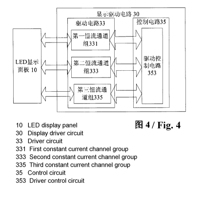
Embodiment 1:
Fig. 4 is a structure diagram of an LED display according to embodiment 1 of
the
invention. As shown in Fig. 4, the LED display includes: an LED display panel
10; and
a display driving circuit 30, the display driving circuit 30 includes a
driving circuit 33
and a control circuit 35, the driving circuit 33 includes a first constant
current channel
group 331, a second constant current channel group 333 and a third constant
current
channel group 335, wherein the first constant current channel group 331
includes one
or more constant current logic components, wherein a first end of each
constant
current logic component is respectively connected with a power end of a first
power
supply equipment 51, a third end of each constant current logic component is
respectively connected with a first R display control sub-port of a driving
control port
of the control circuit, and a second end of each constant current logic
component is
respectively connected with a cathode of an red lamp tube in each LED particle
in a
corresponding column in the LED display panel, and the first constant current
channel group 331 is configured to control the display of the red lamp tubes
of the
LED display panel; the second constant current channel group 333 includes one
or
12 PN30720
CA 02893176 2015-05-29
,
,
, .
more constant current logic components, wherein a first end of each constant
current
logic component is respectively connected with a power end of a second power
supply equipment 53, a third end of each constant current logic component is
respectively connected with a first G display control sub-port of the driving
control
port of the control circuit, and a second end of each constant current logic
component
is respectively connected with a cathode of a green lamp tube in each LED
particle in
a corresponding column in the LED display panel, and the second constant
current
channel group 333 is configured to control the green lamp tubes of the LED
display
panel; the third constant current channel group 335 includes one or more
constant
113 current logic components, wherein a first end of each constant current
logic
component is respectively connected with a power end of a third power supply
equipment, a third end of each constant current logic component is
respectively
connected with a first B display control sub-port of the driving control port
of the
control circuit, and a second end of each constant current logic component is
respectively connected with a cathode of a blue lamp tube in each LED particle
in a
corresponding column in the LED display panel, and the third constant current
channel group 335 is configured to control the blue lamp tubes of the LED
display
panel; the control circuit includes a driving control circuit; wherein the
driving control
circuit is connected with a third end of the driving circuit through the
driving control
port, and is configured to control the switching-on or switching-off of the
driving circuit;
and the driving circuit is configured to control the ordered display of the
LED display
panel.
By the LED display of the invention, the driving circuit 33 and the control
circuit
35 are integrated in the display driving circuit 30, and then more display
driving
circuits 30 can be placed under the condition of not changing the area of the
LED
display panel 10, so that the number ratio of the LED particles to the display
driving
circuits 30 on the LED display with a fixed area is reduced, and the refresh
rate is
increased; moreover, the driving circuit 33 includes the first constant
current channel
group 331, the second constant current channel group 333 and the third
constant
current channel group 335, and the three constant current channel groups
control the
ordered display of the R/G/B LEDs in an LED particle array with M lines and N
columns in the LED display panel 10 respectively, and provide different
working
voltages for the red lamp tubes and the green/blue lamp tubes of the LED
particles in
the LED display panel 10 respectively, so that the power consumption of the
LED
13 PN30720
CA 02893176 2015-05-29
,
. . '
display can be lowered. The problems of large PCB area occupied by the control
circuit 35 and low refresh rate of the LED display in related art are solved,
and the
effects of small PCB area occupied by the control circuit 35, simple design,
high
refresh rate and low power consumption of the LED display are achieved.
Wherein, the first power supply equipment, the second power supply equipment
and the third power supply equipment are not shown in Fig. 4, a power supply
voltage of the first power supply equipment for the first constant current
channel
group preferably is 1.6V, which is obtained by subtracting a typical working
voltage
(1.8-2V) of the red LEDs from a typical working voltages (3.4-3.6V) of the
green/blue
LEDs, and the power supply voltage of the first power supply equipment for the
first
constant current channel group is lower than respective power supply voltages
of the
second power supply equipment and the third power supply equipment for the
second constant current channel group/the third constant current channel
group.
The LED display can include: the LED display panel 10; and the display driving
circuit 30, the display driving circuit 30 includes a switching circuit 31,
the driving
circuit 33 and the control circuit 35, wherein a first end of one of the
switching circuit
31 and the driving circuit 33 is connected to a power end of power supply
equipment,
and a first end of the other of the switching circuit 31 and the driving
circuit 33 is
connected to a grounding end of the power supply equipment; a second end of
one
of the switching circuit 31 and the driving circuit 33 is connected with an
anode of the
LED display panel 10, and a second end of the other of the switching circuit
31 and
the driving circuit 33 is connected with a cathode of the LED display panel
10; the
control circuit 35 includes: a power supply control circuit 351 and a driving
control
353, wherein the power supply control circuit 351 is connected with a third
end of the
switching circuit 31 through a power supply control port, and is configured to
control
the switching-on or switching-off of the switching circuit 31; the driving
control circuit
353 is connected with a third end of the driving circuit 33 through a driving
control
port, and is configured to control the switching-on or switching-off of the
driving circuit
33. Wherein, the switching circuit 31 is configured to control the power
supply of the
LED display panel 10, and the driving circuit 33 is configured to control the
ordered
display of the LED display panel 10.
The switching circuit 31, the driving circuit 33 and the control circuit 35
are
integrated in the display driving circuit 30, and then more display driving
circuits 30
can be placed under the condition of not changing the area of the LED display
panel
14 PN30720
CA 02893176 2015-05-29
'
. .
10, so that the number ratio of the LED particles to the display driving
circuits 30 on
the LED display with a fixed area is reduced, and the refresh rate is
increased; and
the connection relationship between the LED particle array with M lines and N
columns in the LED display panel 10 and the display driving circuits 30 is
clearer, and
fewer connection lines are required, so that the design difficulty of a PCB is
lowered.
The problems of large PCB area occupied by the control circuit 35 and low
refresh
rate of the LED display in related art are solved, and the effects of small
PCB area
occupied by the control circuit 35, simple design and high refresh rate of the
LED
display are achieved.
Fig. 5 is a structure diagram of an LED display according to a preferred
embodiment of the invention; Fig. 5a is a detailed structure diagram of the
LED
display according to the preferred embodiment of the invention shown in Fig.
5; Fig.
5b is a drawing of partial enlargement of a dotted part D in Fig. 5a; and Fig.
5c is a
drawing of partial enlargement of a dotted part D1 in Fig. 5b.
As shown in Fig. 5, the display driving circuit in the display can also
include: the
switching circuit 31, wherein the first end of the switching circuit 31 is
connected to
the grounding end of the power supply equipment, and the second end of the
switching circuit 31 is connected with the anode of the LED display panel; the
control
circuit in the display can also include: the power supply control circuit,
wherein the
power supply control circuit is connected with the third end of the switching
circuit
through the power supply control port, and is configured to control the
switching-on or
switching-off of the switching circuit 31; wherein the switching circuit 31 is
configured
to control the power supply of the LED display panel.
As shown in Fig. 5a, Fig. 5b and Fig. 5c, the switching circuit 31 can include
a
switching sub-circuit, and the switching sub-circuit includes one or more
field effect
transistors, wherein a source of each field effect transistor is connected
with the
power end or the grounding end of the power supply equipment; a drain of each
field
effect transistor is connected with an anode or cathode of each LED particle
in the
corresponding line in the LED display panel 10; and a gate of each field
effect
transistor is connected with a corresponding connection terminal in the power
supply
control port.
According to the above embodiment of the invention, the driving circuit 33 can
include a constant current channel group, and the constant current channel
group
includes one or more constant current logic components, wherein a first end of
each
15 PN30720
CA 02893176 2015-05-29
,
,
, .
constant current logic component is connected with the power end or grounding
end
of the power supply equipment; a second end of each constant current logic
component is connected with the anodes or cathodes of the LED particles in a
corresponding column in the LED display panel 10; and a third end of each
constant
current logic component is connected with the corresponding connection
terminal in
the driving control port.
Specifically, the power supply control circuit 351 is configured to control
each
field effect transistor to be switched on to supply power to the LED particles
in the
line corresponding to the field effect transistor in the LED display panel 10;
and the
driving control circuit 353 is configured to control each constant current
logic
component in the constant current channel group to be switched on, and each
constant current logic component provides a current path for the LED particles
in the
column corresponding to the constant current logic component in the LED
display
panel 10 to control the ordered display of the LED particles after being
switched on.
Specifically, the field effect transistors can be P-MOS transistors, the LED
display panel 10 includes M lines and N columns of LED particles, and each LED
particle respectively includes an red lamp tube, a green lamp tube and a blue
lamp
tube, wherein the anode of the red lamp tube, the anode of the green lamp tube
and
the anode of the blue lamp tube in an ith LED particle in each line are
connected in
parallel with an ith joint, and each joint in each line is connected in
parallel, and is
respectively connected with the drain of the corresponding P-MOS transistor in
the
switching circuit 31; the cathode of the red lamp tube of each LED particle in
each
column is connected in parallel with each other, and is respectively connected
with
the second end of a corresponding constant current logic component in the
constant
current channel group; the cathode of the green lamp tube of each LED particle
in
each column is connected in parallel with each other, and is respectively
connected
with the second end of a corresponding constant current logic component in the
constant current channel group; and the cathode of the blue lamp tube of each
LED
particle in each column is connected in parallel with each other, and is
respectively
connected with the second end of a corresponding constant current logic
component
in the constant current channel group. Wherein, i is more than or equal to 1
and less
than or equal to N, and is a natural number, and the red lamp tubes, the green
lamp
tubes and the blue lamp tubes can be R/G/B LEDs respectively.
Wherein, in the embodiment of the invention, Fig. 5b is a drawing of partial
16 PN30720
CA 02893176 2015-05-29
enlargement of a part D covered by a dotted line in Fig. 5a, the LED particle
shown in
Fig. 5c is a drawing of partial enlargement of a part D1 covered by a dotted
line in Fig.
5b, and in Fig. Sc, pin 1 is a common anode, and pins 2/3/4 are cathodes of
the
B/G/R LEDs respectively.
The display driving circuit 30 includes a switching sub-circuit, the constant
current channel group and the control circuit 35. The switching sub-circuit 31
includes
N P-MOS transistors, wherein the drain of each P-MOS transistor serves as one
of
output pins of the control circuit 35, the source of each P-MOS transistor is
connected to a power supply end (i.e. VCC end) of the display driving circuit
30, and
the gate of each P-MOS transistor is connected with a connection terminal in
the
power supply control port of the control circuit 35; the constant current
channel group
can include N constant current logic components (which can also be called
constant
current logic circuits), the second end (input end of the constant current
logic
component in the embodiment) of each constant current logic component serves
as
one of input pins of the display driving circuit 30, the first ends (i.e.
output ends) of all
the constant current logic components are internally interconnected, and are
connected with the grounding end of the power supply equipment as a grounding
end
(i.e. GND end) of the display driving circuit 30, and the third ends (control
ends of the
constant current logic components in the embodiment) of the constant current
logic
components are connected with the driving control port of the control circuit
35, and
are configured to receive a constant current control signal of the driving
circuit 33.
In embodiment 1, the LED display panel 10 (which can be called an LED unit as
well as an LED unit board) includes a matrix with M lines and N columns of LED
particles, wherein the anodes of the LED particles in each line are
interconnected to
the ith joint, each joint is connected to the output pin corresponding to the
drain of the
corresponding P-MOS transistor in the switching sub-circuit 31 in the
switching circuit
31 and the cathodes of the LEDs in the same primary colors in the LED
particles in
each column are interconnected to the input ends of the corresponding constant
current logic components of the constant current channel group of the display
driving
circuit 30, that is, the common cathode of the red lamp tubes (i.e. R LEDs) in
the LED
particles in each column is interconnected to the input end of the
corresponding
constant current logic component of the constant current channel group of the
display
driving circuit 30; the common cathode of the green lamp tubes (i.e. G LEDs)
in the
LED particles in each column is interconnected to the input end of the
corresponding
17 PN30720
CA 02893176 2015-05-29
constant current logic component of the constant current channel group of the
display
driving circuit 30; and the common cathode of the blue lamp tubes (i.e. B
LEDs) in
the LED particles in each column is interconnected to the input end of the
corresponding constant current logic component of the constant current channel
group of the display driving circuit 30.
According to the LED display panel 10, under the control of the display
driving
circuit 30, the power supply control circuit 351 controls a certain P-MOS
transistor in
the switching sub-circuit 31 (which can be the P-MOS channel group) to be in
an on
state through the power supply control port to supply power to the anodes of
the LED
particles in the corresponding line on the LED display panel 10, and the
driving
control circuit 353 outputs a constant current control signal to each constant
current
logic component in the constant current channel group through the driving
control
port to control each constant current logic component to be in an on working
state,
thereby providing the current paths for the cathodes of the LED particles in
the
corresponding columns and realizing the ordered display of the LED unit.
Wherein,
the cathodes of the LED particles in the corresponding columns include the
cathodes
of the R, G and B three primary colors lamp tubes, that is, the ordered
display of the
red lamp tubes, the green lamp tubes and the blue lamp tubes of the LED
particles in
the corresponding columns respectively.
In the embodiment of the invention, the field effect transistors can be P-MOS
transistors, the LED display panel 10 includes M lines and N columns of LED
particles, and each LED particle includes an red lamp tube, a green lamp tube
and a
blue lamp tube, wherein the anode of the red lamp tube, the anode of the green
lamp
tube and the anode of the blue lamp tube in each LED particle in each line are
connected in parallel, and are connected with the drain of the corresponding P-
MOS
transistor in the switching circuit 31; the cathode of the red lamp tube of
each LED
particle in each column is connected in parallel, and is connected with the
second
end of the corresponding constant current logic component in the constant
current
channel group; the cathode of the green lamp tube of each LED particle in each
column is connected in parallel, and is connected with the second end of the
corresponding constant current logic component in the constant current channel
group; and the cathode of the blue lamp tube of each LED particle in each
column is
connected in parallel, and is connected with the second end of the
corresponding
constant current logic component in the constant current channel group.
18 PN30720
CA 02893176 2015-05-29
Based on the technical solution shown in embodiment 1, there can be a first
transformed implementation mode as follows:
the anodes of the R/G/B LEDs of the LED particles in each line in the LED
display panel 10 are interconnected to the output pin corresponding to the
drain of a
corresponding P-MOS transistor in the switching circuit 31 in the display
driving
circuit 30, and the cathodes of the LEDs in the same primary colors in the LED
particles in each column are interconnected to the input ends of the constant
current
logic components of the constant current channel group of the display driving
circuit
30, that is, the common cathode of the R LEDs in the LED particles in each
column is
interconnected to the input end of the constant current logic component of the
constant current channel group of the display driving circuit 30; the common
cathode
of the G LEDs in the LED particles in each column is interconnected to the
input end
of the constant current logic component of the constant current channel group
of the
display driving circuit 30; and the common cathode of the B LEDs in the LED
particles in each column is interconnected to the input end of the constant
current
logic component of the constant current channel group of the display driving
circuit
30.
In the transformed mode, a connection relationship of the anodes of the LED
particles in each line in the LED display panel 10 rather than a control mode
of the
display driving circuit 30 is changed, and in the transformed mode, the anodes
of the
R/G/B LEDs of the LED particles in each line are directly interconnected, and
are
connected to the output pin corresponding to the drain of a corresponding P-
MOS
transistor in the switching circuit. In the transformed mode, the switching
circuit 31,
the driving circuit 33 and the control circuit 35 are integrated in the
display driving
circuit 30, and then more display driving circuits 30 can be placed under the
condition
of not changing the area of the LED display panel 10, so that the number ratio
of the
LED particles and the display driving circuits 30 on the LED display with the
fixed
area is reduced, and the refresh rate is increased; moreover, the connection
relationship between the LED particle array in the LED display panel 10 and
the
display driving circuits 30 is clearer, and fewer connection lines are
required, so that
the design difficulty of the PCB is lowered.
Based on the technical solution shown in embodiment 1, there can also be a
second transformed implementation mode as follows:
the field effect transistors can also be N-channel Metal Oxide Semiconductor
19 PN30720
CA 02893176 2015-05-29
'
,
(N-MOS) transistors, the LED display panel 10 can include M lines and N
columns of
LED particles, and each LED particle includes an red lamp tube, a green lamp
tube
and a blue lamp tube, wherein the cathode of the red lamp tube, the cathode of
the
green lamp tube and the cathode of the blue lamp tube in the ith LED particle
in each
line are connected in parallel with the ith joint, and each joint in each line
is
connected in parallel, and is connected with a drain of the corresponding N-
MOS
transistor in the switching circuit 31; the anode of the red lamp tube in each
LED
particle in each column is connected in parallel, and is connected with the
second
end of the corresponding constant current logic component in the constant
current
channel group; the anode of the green lamp tube of each LED particle in each
column is connected in parallel, and is connected with the second end of the
corresponding constant current logic component in the constant current channel
group; and the anode of the blue lamp tube of each LED particle in each column
is
connected in parallel, and is connected with the second end of the
corresponding
constant current logic component in the constant current channel group.
Wherein, i is
more than or equal to 1 and less than or equal to N, and is a natural number.
Specifically, in the second transformed mode, the switching sub-circuit
includes
N N-MOS transistors, wherein the drain of each N-MOS transistor serves as one
of
output pins of the control circuit 35, the source of each N-MOS transistor is
connected with the grounding end of the power supply equipment as the
grounding
end (i.e. GND end) of the display driving circuit 30, and the gate of each N-
MOS
transistor is connected with a connection terminal in the power supply control
port of
the control circuit 35; the constant current channel group includes N constant
current
logic components (which can also be called constant current logic circuits),
the
second end (i.e. input end) of each constant current logic component serves as
one
of the input pins of the display driving circuit 30, the first ends (i.e.
output ends) of all
the constant current logic components are internally interconnected, and are
connected with the grounding end of the power supply equipment as the power
supply end (i.e. VCC end) of the display driving circuit 30, and the third
ends (i.e.
control ends) of the constant current logic components are connected with the
display
control port of the control circuit 35, and are configured to receive the
constant
current control signal of the driving circuit 33.
In the second transformed mode, the LED display panel 10 (which can also be
called an LED unit) includes a matrix with M lines and N columns of LED
particles,
20 PN30720
CA 02893176 2015-05-29
'
'
, .
wherein the cathodes of the LED particles in each line are interconnected to
the ith
joint, each joint is connected to the output pin corresponding to the drain of
the
corresponding N-MOS transistor in the switching circuit 31 in the display
driving
circuit 30, and the anodes of the LEDs in the same primary colors in the LED
particles in each column are interconnected to the input ends of the
corresponding
constant current logic components of the constant current channel group of the
display driving circuit 30, that is, the common anode of the R LEDs in the LED
particles in each column is interconnected to the input end of the
corresponding
constant current logic component of the constant current channel group of the
display
11:1 driving circuit 30; the common anode of the G LEDs in the LED
particles in each
column is interconnected to the input end of the corresponding constant
current logic
component of the constant current channel group of the display driving circuit
30; and
the common anode of the B LEDs in the LED particles in each column is
interconnected to the input end of the corresponding constant current logic
component of the constant current channel group of the display driving circuit
30.
In the second transformed mode, the power supply control circuit 351 in the
display driving circuit 30 controls any one N-MOS transistor in the switching
circuit 31
to be in an on state through the power supply control port to supply power to
the
anodes of the LED particles in the corresponding line on the LED display panel
10,
and the driving control circuit 353 outputs the constant current control
signal to each
constant current logic component in the constant current channel group through
the
driving control port to control each constant current logic component to be in
an on
working state, thereby providing the current path for the anodes of the LED
particles
in the corresponding columns and realizing the ordered display of the LED
unit.
Wherein, the anodes of the lamp tubes of the LED particles in the
corresponding
columns include the anodes of three primary colors R, G and B, that is, the
ordered
display of the red lamp tubes, the green lamp tubes and the blue lamp tubes of
the
LED particles in the corresponding columns is also controlled respectively.
Based on the technical solution shown in the second transformed mode of
embodiment 1, there can also be a transformed implementation mode as follows:
the field effect transistors can be N-MOS transistors, the LED display panel
10
can include M lines and N columns of LED particles, and each LED particle
includes
an red lamp tube, a green lamp tube and a blue lamp tube, wherein the cathode
of
the red lamp tube, the cathode of the green lamp tube and the cathode of the
blue
21 PN30720
CA 02893176 2015-05-29
lamp tube in each LED particle in each line are connected in parallel, and are
connected with the drain of the corresponding N-MOS transistor in the
switching
circuit 31; the anode of the red lamp tube of each LED particle in each column
is
connected in parallel, and is connected with the second end of the
corresponding
constant current logic component in the constant current channel group; the
anode of
the green lamp tube of each LED particle in each column is connected in
parallel,
and is connected with the second end of the corresponding constant current
logic
component in the constant current channel group; and the anode of the blue
lamp
tube of each LED particle in each column is connected in parallel, and is
connected
with the second end of the corresponding constant current logic component in
the
constant current channel group.
Specifically, the cathodes of the LED particles in each line in the LED
display
panel 10 in the implementation mode can be interconnected to the output pin
corresponding to the drain of the corresponding N-MOS transistor in the
switching
circuit 31 in the display driving circuit 30, and the anodes of the LEDs in
the same
primary colors in the LED particles in each column are interconnected to the
input
ends of the corresponding constant current logic components of the constant
current
channel group of the display driving circuit 30, that is, the common anode of
the R
LEDs of red lamp tubes in the LED particles in each column is interconnected
to the
input end of the corresponding constant current logic component of the
constant
current channel group of the display driving circuit 30; the common anode of
the G
LEDs in the LED particles in each column is interconnected to the input end of
the
corresponding constant current logic component of the constant current channel
group of the display driving circuit 30; and the common anode of the B LEDs in
the
LED particles in each column is interconnected to the input end of the
corresponding
constant current logic component of the constant current channel group of the
display
driving circuit 30.
Based on the technical solution shown in embodiment 1, there can also be a
third transformed implementation mode as follows:
in the implementation mode, the driving circuit 33 can include a first
constant
current channel group, a second constant current channel group and a third
constant
current channel group, wherein the first constant current channel group
includes one
or more constant current logic components, a first end of each constant
current logic
component is connected with the power end or grounding end of the power supply
22 PN30720
CA 02893176 2015-05-29
. .
equipment, a third end of each constant current logic component is connected
with a
first R display control sub-port of the driving control port, and a second end
of each
constant current logic component is connected with the anode or cathode of the
red
lamp tube in each LED particle in the corresponding column in the LED display
panel
10, and is configured to control the display of the red lamp tubes of the LED
display
panel 10; the second constant current channel group includes one or more
constant
current logic components, a first end of each constant current logic component
is
connected with the power end or grounding end of the power supply equipment, a
third end of each constant current logic component is connected with a first G
display
control sub-port of the driving control port, and a second end of each
constant current
logic component is connected with the anode or cathode of the green lamp tube
in
each LED particle in the corresponding column in the LED display panel 10, and
is
configured to control the display of the green lamp tubes of the LED display
panel 10;
and the third constant current channel group includes one or more constant
current
logic components, a first end of each constant current logic component is
connected
with the power end or grounding end of the power supply equipment, a third end
of
each constant current logic component is connected with a first B display
control
sub-port of the driving control port, and a second end of each constant
current logic
component is connected with the anode or cathode of the blue lamp tube in each
LED particle in the corresponding column in the LED display panel 10, and is
configured to control the display of the blue lamp tubes of the LED display
panel 10.
Wherein, the first constant current channel group can be an R constant current
channel group, the second constant current channel group can be a G constant
current channel group, and the third constant current channel group can be a B
constant current channel group.
Specifically, the R constant current channel group can include one or more
constant current logic components, the second ends (i.e. input ends) of these
constant current logic components are connected to the cathodes (i.e. R
cathodes) of
the red lamp tubes of the LED particles in the corresponding columns in the
LED
display panel 10, the first ends (i.e. output ends) of the constant current
logic
components are interconnected as an external pin GND of the display driving
circuit
30, and are connected to the grounding end of the power supply equipment, and
the
third ends (i.e. control ends) of the constant current logic components are
connected
to the first R display control sub-port of the driving control port to receive
an R display
23 PN30720
CA 02893176 2015-05-29
control signal of the driving control circuit 353; the G constant current
channel group
can include one or more constant current logic components, the second ends
(i.e.
input ends) of these constant current logic components are connected to the
cathodes (i.e. G cathodes) of the green lamp tubes of the LED particles in the
corresponding columns in the LED display panel 10, the first ends (i.e. output
ends)
of the constant current logic components are interconnected as the external
pin GND
of the display driving circuit 30, and are connected to the grounding end of
the power
supply equipment, and the third ends (i.e. control ends) of the constant
current logic
components are connected to the first G display control sub-port of the
driving control
port to receive a G display control signal of the driving control circuit 353;
and the B
constant current channel group can include one or more constant current logic
components, the second ends (i.e. input ends) of these constant current logic
components are connected to the cathodes (i.e. B cathodes) of the blue lamp
tubes
of the LED particles in the corresponding columns in the LED display panel 10,
the
first ends (i.e. output ends) of the constant current logic components are
interconnected as the external pin GND of the display driving circuit 30, and
are
connected to the grounding end of the power supply equipment, and the third
ends
(i.e. control ends) of the constant current logic components are connected to
the first
B display control sub-port of the driving control port to receive a B display
control
signal of the driving control circuit 353.
In the implementation mode, the power supply control circuit 351 controls each
field effect transistor to be switched on to supply power to the LED particles
in the
lines corresponding to the field effect transistors in the LED display panel
10; the
driving control circuit 353 is configured to control each constant current
logic
component in the first constant current channel group to be switched on
through the
first R display control sub-port, and each constant current logic component
provides a
current path for the red lamp tubes in the LED particles in the column
corresponding
to the constant current logic component in the LED display panel 10 to control
the
display of the red lamp tubes of the LED particles in the line corresponding
to the
field effect transistor in the LED display panel 10 after being switched on;
the driving
control circuit 353 is further configured to control each constant current
logic
component in the second constant current channel group to be switched on
through
the first G display control sub-port, and each constant current logic
component
provides a current path for the green lamp tubes in the LED particles in the
column
24 PN30720
CA 02893176 2015-05-29
,
. .
corresponding to the constant current logic component in the LED display panel
10 to
control the display of the green lamp tubes of the LED particles in the line
corresponding to the field effect transistor in the LED display panel 10 after
being
switched on; and the driving control circuit 353 is further configured to
control each
constant current logic component in the third constant current channel group
to be
switched on through the first B display control sub-port, and each constant
current
logic component provides a current path for the blue lamp tubes in the LED
particles
in the column corresponding to the constant current logic component in the LED
display panel 10 to control the display of the blue lamp tubes of the LED
particles in
the line corresponding to the field effect transistor in the LED display panel
10 after
being switched on.
In the implementation mode, the power supply control port of the display
driving
circuit 30 is unchanged, and the driving control port includes three control
sub-ports
for controlling the switching-on or switching-off of the first/second/third
constant
current channel groups to enable the switching circuit and the driving circuit
to control
the power supply of the LED particles in each line and the ordered display of
the LED
particles in each column in the LED display panel respectively. In the
transformed
mode, the switching circuit 31, the driving circuit 33 and the control circuit
35 are
integrated in the display driving circuit 30, only the driving circuit
includes the three
constant current channel groups, and more display driving circuits 30 can
still be
placed under the condition of not changing the area of the LED display panel
10, so
that the number ratio of the LED particles and the display driving circuits 30
on the
LED display with the fixed area is reduced, and the refresh rate is increased;
moreover, the connection relationship between the LED particle array in the
LED
display panel 10 and the display driving circuits 30 is clearer, and fewer
connection
lines are required, so that the design difficulty of the PCB is lowered.
In the implementation mode, the field effect transistors can be P-MOS
transistors,
the LED display panel 10 includes M lines and N columns of LED particles, and
each
LED particle includes an red lamp tube, a green lamp tube and a blue lamp
tube,
wherein the anode of the red lamp tube, the anode of the green lamp tube and
the
anode of the blue lamp tube in the ith LED particle in each line are connected
in
parallel to the ith joint, and each joint in each line is connected in
parallel, and is
connected with the drain of the corresponding P-MOS transistor in the
switching
circuit 31; the cathode of the red lamp tube of each LED particle in each
column is
25 PN30720
CA 02893176 2015-05-29
,
,
connected in parallel, and is connected with the second end of the
corresponding
constant current logic component in the first constant current channel group;
the
cathode of the green lamp tube of each LED particle in each column is
connected in
parallel, and is connected with the second end of the corresponding constant
current
logic component in the second constant current channel group; and the cathode
of
the blue lamp tube of each LED particle in each column is connected in
parallel, and
is connected with the second end of the corresponding constant current logic
component in the third constant current channel group. Wherein, i is more than
or
equal to 1 and less than or equal to N, and is a natural number, and the red
lamp
tubes, the green lamp tubes and the blue lamp tubes can be the R/G/B LEDs
respectively.
In addition, the LED display panel 10 (which can also be called an LED unit)
includes a matrix with M lines and N columns of LED particles, wherein the
anodes of
the LED particles in each line are interconnected to the ith joint, each joint
is
connected to the output pin corresponding to the drain of the corresponding P-
MOS
transistor in the switching circuit 31 in the display driving circuit 30, and
the cathodes
of the LEDs in the same primary colors in the LED particles in each column are
interconnected to the input ends of the corresponding constant current logic
components of the first constant current channel group of the display driving
circuit
30, that is, the common cathode of the R LEDs in the LED particles in each
column is
interconnected to the input end of the constant current logic component of the
second
constant current channel group of the display driving circuit 30; the common
cathode
of the G LEDs in the LED particles in each column is interconnected to the
input end
of the constant current logic component of the constant current channel group
of the
display driving circuit 30; and the common cathode of the B LEDs in the LED
particles in each column is interconnected to the input end of the constant
current
logic component of the third constant current channel group of the display
driving
circuit 30.
In the embodiment, the power supply control circuit 351 of the display driving
circuit 30 controls any one P-MOS transistor in the switching circuit 31 to be
in an on
state through the power supply control port to supply power to the anodes of
the LED
particles in the corresponding line on the LED display panel 10, and the
driving
control circuit 353 outputs an R display control signal/G display control
signal/B
display control signal to each constant current logic component in the first
constant
26 PN30720
CA 02893176 2015-05-29
'
,
. ,
current channel group/second constant current channel group/third constant
current
channel group through the first R display control sub-port/first G display
control
sub-port/first B display control sub-port to control each constant current
logic
component in the three constant current channel groups to be in an on working
state,
thereby providing the current paths for the R cathodes, G cathodes and B
cathodes
of the LED particles in the corresponding columns and realizing the ordered
display
of the LED particles. Wherein, the R cathodes, G cathodes and B cathodes of
the
LED particles in the corresponding columns are the cathodes of the red lamp
tubes,
the green lamp tubes and the green lamp tubes of the LED particles in the
corresponding columns respectively. Wherein, the switching sub-circuit can
also be
called a P-MOS channel.
Based on the technical solution shown in the third transformed implementation
mode of embodiment 1, there can also be a transformed implementation mode as
follows:
the field effect transistors can be P-MOS transistors, the LED display panel
10
can include M lines and N columns of LED particles, and each LED particle
includes
an red lamp tube, a green lamp tube and a blue lamp tube, wherein the anodes
of
the red lamp tube, the anodes of the green lamp tube and the anodes of the
blue
lamp tube in each LED particle in each line are connected in parallel, and are
connected with the drain of the corresponding P-MOS transistor in the
switching
circuit 31; the cathode of the red lamp tube of each LED particle in each
column is
connected in parallel, and is connected with the second end of the
corresponding
constant current logic component in the first constant current channel group;
the
cathode of the green lamp tube of each LED particle in each column is
connected in
parallel, and is connected with the second end of the corresponding constant
current
logic component in the second constant current channel group; and the cathode
of
the blue lamp tube of each LED particle in each column is connected in
parallel, and
is connected with the second end of the corresponding constant current logic
component in the third constant current channel group.
Specifically, the anodes of the LED particles in each line in the LED display
panel
10 are interconnected to the output pin corresponding to the drain of a
corresponding
P-MOS transistor in the switching circuit 31 in the display driving circuit
30, and the
cathodes of the LEDs in the same primary colors in the LED particles in each
column
are interconnected to the input ends of the constant current logic components
of the
27 PN30720
CA 02893176 2015-05-29
,
first constant current channel group of the display driving circuit 30, that
is, the
common cathode of the R LEDs in the LED particles in each column is
interconnected to the input end of the constant current logic component of the
second
constant current channel group of the display driving circuit 30; the common
cathode
of the G LEDs in the LED particles in each column is interconnected to the
input end
of the constant current logic component of the constant current channel group
of the
display driving circuit 30; and the common cathode of the B LEDs in the LED
particles in each column is interconnected to the input end of the constant
current
logic component of the third constant current channel group of the display
driving
circuit 30.
In the implementation mode, the control mode is the same as that of the
display
driving circuit 30 in the technical solution shown in the third transformed
implementation mode of embodiment 1, and similarly, the power supply control
circuit
351 controls a certain P-MOS transistor in the switching circuit 31 (i.e. the
P-MOS
channel group) to be in an on state through the power supply control port to
supply
power to the anodes of the LED particles in the corresponding line on the LED
display panel 10, and the driving control circuit 353 outputs the R display
control
signal/G display control signal/B display control signal to each constant
current logic
component in the first constant current channel group/second constant current
channel group/third constant current channel group through the first R display
control
sub-port/first G display control sub-port/first B display control sub-port to
control each
constant current logic component in the three constant current channel groups
to be
in an on working state, thereby providing the current paths for the R
cathodes, G
cathodes and B cathodes of the LED particles in the corresponding columns and
realizing the ordered display of the LED particles. Wherein, the R cathodes, G
cathodes and B cathodes of the LED particles in the corresponding columns are
the
cathodes of the red lamp tubes, the green lamp tubes and the blue lamp tubes
of the
LED particles in the corresponding columns respectively.
Embodiment 2:
Fig. 6a to Fig. 6c are structure diagrams of an LED display according to
embodiment 2 of the invention. As shown in Fig. 6a, field effect transistors
in the LED
display can also be N-MOS transistors, an LED display panel 10 can include M
lines
and N columns of LED particles, and each LED particle includes an red lamp
tube, a
green lamp tube and a blue lamp tube, wherein a cathode of the red lamp tube,
a
28 PN30720
CA 02893176 2015-05-29
=
. .
cathode of the green lamp tube and a cathode of the blue lamp tube in an ith
LED
particle in each line are connected in parallel with an ith joint, and each
joint in each
line is connected in parallel, and is connected with a drain of a
corresponding N-MOS
transistor in a switching circuit 31 respectively; an anode of the red lamp
tube in each
LED particle in each column is connected in parallel respectively, and is
connected
with the second end of a corresponding constant current logic component in the
first
constant current channel group respectively as a connection terminal of an
anode of
the LED display panel 10; an anode of the green lamp tube of each LED particle
in
each column is connected in parallel respectively, and is connected with the
second
end of a corresponding constant current logic component in the second constant
current channel group respectively as a connection terminal of the anode of
the LED
display panel 10; and an anode of the blue lamp tube of each LED particle in
each
column is connected in parallel respectively, and is connected with the second
end of
a corresponding constant current logic component in the third constant current
channel group respectively as a connection terminal of the anode of the LED
display
panel 10.
Specifically, as shown in Fig. 6a, the R constant current channel group can
include one or more constant current logic components, first ends (input ends
in the
embodiment) of these constant current logic components are interconnected as
an
external pin VCCR of the display driving circuit 30, and are connected to a
power end
of a power supply equipment, second ends (i.e. output ends) of the constant
current
logic components are connected to the anodes (R anodes in the embodiment) of
the
red lamp tubes of the LED particles in the corresponding columns in the LED
display
panel 10, and third ends (i.e. control ends) of the constant current logic
components
are connected to a first R display control port; the G constant current
channel group
can include one or more constant current logic components, first ends (input
ends in
the embodiment) of these constant current logic components are interconnected
as
an external pin VCCG of the display driving circuit 30, and are connected to a
power
end of the power supply equipment, second ends (i.e. output ends) of the
constant
current logic components are connected to the anodes (G anodes in the
embodiment)
of the green lamp tubes of the LED particles in the corresponding columns in
the LED
display panel 10, and third ends (i.e. control ends) of the constant current
logic
components are connected to a first G display control port; and the B constant
current channel group can include one or more constant current logic
components,
29 PN30720
CA 02893176 2015-05-29
first ends (input ends in the embodiment) of the constant current logic
components
are interconnected as an external pin VCCB of the display driving circuit 30,
and are
connected to the power end of the power supply equipment, second ends (i.e.
output
ends) of the constant current logic components are connected to the anodes (B
anodes in the embodiment) of the blue lamp tubes of the LED particles in the
corresponding columns in the LED display panel 10, and third ends (i.e.
control ends)
of the constant current logic components are connected to a first B display
control
port.
The LED particle shown in Fig. 6c is a drawing of partial enlargement of a
part
El covered by a dotted line in Fig. 6b, wherein pin 4 is a common cathode, and
pins
2/3/4 are the anodes of R/G/B LEDs respectively.
Wherein, in the embodiment, a power supply voltage of the external pin VCCR of
the display driving circuit 30 can be lower than that of the external pin
VCCR/VCCB,
and specifically, the power supply voltage of the VCCR can be 1.6V which is
obtained
by subtracting a working voltage (1.8-2V) of the red lamp tubes from a working
voltages (3.4-3.6V) of the green and blue lamp tubes, and the power supply
voltages
of the R/G/B LEDs are differentially controlled, thereby reducing the power
consumption of the LED display.
In embodiment 2, the LED display panel 10 (which can also be called an LED
unit) includes a matrix with M lines and N columns of LED particles, wherein
the
cathodes of the LED particles in each line are interconnected to the ith
joint, each
joint is connected to an output pin corresponding to the drain of the
corresponding
N-MOS transistor in the switching circuit 31 in the display driving circuit
30, and the
anodes of the LEDs in the same primary colors in the LED particles in each
column
are interconnected to the input ends of the corresponding constant current
logic
components of the constant current channel group of the display driving
circuit 30,
that is, the common anode of the R LEDs in the LED particles in each column is
interconnected to the input end of the corresponding constant current logic
component of the second constant current channel group of the display driving
circuit
30; the common anode of the G LEDs in the LED particles in each column is
interconnected to the input end of the corresponding constant current logic
component of the constant current channel group of the display driving circuit
30; and
the common anode of the B LEDs in the LED particles in each column is
interconnected to the input end of the corresponding constant current logic
30 PN30720
CA 02893176 2015-05-29
'
. ,
component of the third constant current channel group of the display driving
circuit 30.
Under the control of the display driving circuit 30, the power supply control
circuit 351
controls a certain N-MOS transistor in the switching sub-circuit 31 (which can
be an
N-MOS channel group) to be in an on state through a power supply control port
to
supply power to the anodes of the LED particles in the corresponding line on
the LED
display panel 10, and the driving control circuit 353 outputs an R display
control
signal/G display control signal/B display control signal to each constant
current logic
component in the first constant current channel group/second constant current
channel group/third constant current channel group through the first R display
control
sub-port/first G display control sub-port/first B display control sub-port to
control each
constant current logic component in the three constant current channel groups
to be
in an on working state respectively, thereby providing the current paths for
the R
anodes, G anodes and B anodes of the LED particles in the corresponding
columns
and realizing the ordered display of the LED particles. Wherein, the R anodes,
G
anodes and B anodes of the LED particles in the corresponding columns are the
anodes of the red lamp tubes, the green lamp tubes and the blue lamp tubes of
the
LED particles in the corresponding columns respectively.
Embodiments 3 and 4:
Fig. 7a to Fig. 7e are structure diagrams of an LED display according to
embodiment 3 of the invention; and Fig. 8a to Fig. 8c are structure diagrams
of an
LED display according to embodiment 4 of the invention. Fig. 7b and Fig. 8b
show
drawings of partial enlargement of a part F covered by a dotted line in Fig.
7a and a
part H covered by a dotted line in Fig. 8a in the two embodiments
respectively, LEDs
of three primary colors in an LED particle in Fig. 7c are directly integrated
on the LED
particle, LEDs in three primary colors in an LED particle in Fig. 8c are
encapsulated
and integrated on the LED particle respectively, but beyond that, the same
circuit
connection relationship can be adopted in the two implementation modes.
Wherein,
an anode of each LED particle in Fig. 7c has three pins, i.e. 1, 2 and 3
respectively,
corresponding to anodes of internal R/G/B LEDs respectively, and a cathode of
each
LED particle in Fig. 7c has three pins, i.e. 4, 5 and 6 respectively,
corresponding to
cathodes of the internal B/G/R LEDs respectively; and as shown in Fig. 8c, the
anodes of the R/G/B LEDs are pins 1, the cathodes of the R/G/B LEDs are pins
2,
and the R/G/B LEDs are welded in parallel as the LED particles (i.e. full-
color pixels).
Specifically, as shown in Fig. 7e and Fig. 8a, field effect transistors can
also be
31 PN3 0720
CA 02893176 2015-05-29
N-MOS transistors, an LED display panel 10 can include M lines and N columns
of
LED particles, and each LED particle includes an red lamp tube, a green lamp
tube
and a blue lamp tube respectively, wherein the cathode of the red lamp tube,
the
cathode of the green lamp tube and the cathode of the blue lamp tube in each
LED
particle in each line are connected in parallel, and are connected with the
drain of a
corresponding N-MOS transistor in a switching circuit 31 respectively; the
anode of
the red lamp tube in each LED particle in each column is connected in parallel
respectively, and is connected with the second end of a corresponding constant
current logic component in a first constant current channel group
respectively; the
anode of the green lamp tube of each LED particle in each column is connected
in
parallel respectively, and is connected with the second end of a corresponding
constant current logic component in a second constant current channel group
respectively; and the anode of the blue lamp tube of each LED particle in each
column is connected in parallel respectively, and is connected with the second
end of
a corresponding constant current logic component in a third constant current
channel
group respectively.
In embodiments 3 and 4, the anodes of the LED particles in each line in the
LED
display panel 10 are interconnected to an output pin corresponding to the
drain of the
corresponding N-MOS transistor in the switching circuit 31 in the display
driving
circuit 30, the cathodes of the LED particles in each line are interconnected
to an ith
joint, each joint is connected to the output pin corresponding to the drain of
the
corresponding N-MOS transistor in the switching circuit 31 in the display
driving
circuit 30, and the anodes of the LEDs in the same primary colors in the LED
particles in each column are interconnected to the input ends of the
corresponding
constant current logic components of the first constant current channel group
of the
display driving circuit 30, that is, the common anode of the R LEDs in the LED
particles in each column is interconnected to the input end of the constant
current
logic component of the second constant current channel group of the display
driving
circuit 30; the common anode of the G LEDs in the LED particles in each column
is
interconnected to the input end of the constant current logic component of the
constant current channel group of the display driving circuit 30; and the
common
cathode of the B LEDs in the LED particles in each column is interconnected to
the
input end of the constant current logic component of the third constant
current
channel group of the display driving circuit 30.
32 PN30720
CA 02893176 2015-05-29
'
. ,
Based on the technical solutions shown in embodiments 3 and 4, there can also
be a first transformed implementation mode as follows:
in the implementation mode, the switching circuit 31 includes a first
switching
sub-circuit and a second switching sub-circuit, each of the first switching
sub-circuit
and the second switching sub-circuit includes one or more field effect
transistors, and
a source of each field effect transistor in the first switching sub-circuit
and the second
switching sub-circuit is connected with a power end or grounding end of a
power
supply equipment respectively, wherein a drain of each field effect transistor
in the
first switching sub-circuit is connected with the anode or cathode of the red
lamp tube
in each LED particle in the corresponding line in the LED display panel
respectively,
and a gate of each field effect transistor is connected with a corresponding
connection terminal in a power supply control port respectively, and is
configured to
control the power supply of the red lamp tubes of the LED display panel; and a
drain
of each field effect transistor in the second switching sub-circuit is
connected with the
anodes or cathodes of the green lamp tube and the blue lamp tube in each LED
particle in the corresponding line in the LED display panel respectively, and
a gate of
each field effect transistor is connected with a corresponding connection
terminal in
the power supply control port respectively, and is configured to control the
power
supply of the green lamp tubes and the blue lamp tubes of the LED display
panel.
In the implementation mode, the driving circuit 33 can include a constant
current
channel group, and the constant current channel group can include: one or more
constant current logic components, wherein a first end of each constant
current logic
component is connected with the power end or grounding end of the power supply
equipment; a second end of each constant current logic component is connected
with
the anodes or cathodes of the LED particles in the corresponding column in the
LED
display panel 10; and a third end of each constant current logic component is
connected with the corresponding connection terminal in the driving control
port.
In addition, in the embodiment, the power supply control circuit 351 is
configured
to control one field effect transistor in the first switching sub-circuit to
be switched on
to supply power to the red lamp tubes in the LED particles in the line
corresponding
to the field effect transistor in the first switching sub-circuit in the LED
display panel
10; the power supply control circuit 351 is further configured to control the
field effect
transistor corresponding to the switched-on field effect transistor in the
first switching
sub-circuit in the second switching sub-circuit to be switched on to supply
power to
33 PN30720
CA 02893176 2015-05-29
. ,
the green lamp tubes and the blue lamp tubes in the LED particles in the line
corresponding to the field effect transistor in the first switching sub-
circuit in the LED
display panel 10; and the driving control circuit 353 is configured to control
each
constant current logic component in the constant current channel group to be
switched on, and each constant current logic component provides a current path
for
the LED particles in the column corresponding to the constant current logic
component in the LED display panel 10 to control the ordered display of the
LED
particles in the line corresponding to the field effect transistor in the LED
display
panel 10 respectively after being switched on.
The switching circuit 31, the driving circuit 33 and the control circuit 35
are
integrated in the display driving circuit 30, and then more display driving
circuits 30
can be placed under the condition of not changing the area of the LED display
panel
10, so that the number ratio of the LED particles and the display driving
circuits 30 on
the LED display with the fixed area is reduced, and the refresh rate is
increased.
The field effect transistors of the display driving circuit 30 in the
embodiment can
be P-MOS transistors, the LED display panel 10 can include M lines and N
columns
of LED particles, and each LED particle includes an red lamp tube, a green
lamp tube
and a blue lamp tube, wherein the anode of the red lamp tube in the ith LED
particle
in each line is connected in parallel with the ith joint, and each joint in
each line is
connected in parallel, and is connected with the drain of a corresponding P-
MOS
transistor in the first switching sub-circuit 31 respectively; the anodes of
the green
lamp tube and the anodes of the blue lamp tube in the jth LED particle in each
line
are connected in parallel with a jth joint, and each joint in each line is
connected in
parallel, and is connected with the drain of a corresponding P-MOS transistor
in the
second switching sub-circuit 31; the cathode of the red lamp tube of each LED
particle in each column is connected in parallel, and is connected with the
second
end of a corresponding constant current logic component in the constant
current
channel group respectively; the cathode of the green lamp tube of each LED
particle
in each column is connected in parallel, and is connected with the second end
of a
corresponding constant current logic component in the constant current channel
group respectively; and the cathode of the blue lamp tube of each LED particle
in
each column is connected in parallel, and is connected with the second end of
a
corresponding constant current logic component in the constant current channel
group respectively. Wherein, i is more than or equal to 1 and less than or
equal to N, j
34 PN30720
CA 02893176 2015-05-29
is more than or equal to 1 and less than or equal to N, both i and j are
natural
numbers, and the red lamp tubes, the green lamp tubes and the blue lamp tubes
can
be R/G/B LEDs respectively.
In the implementation mode, the display driving circuit 30 integrates the
first
switching sub-circuit and the second switching sub-circuit, and each of the
two
switching sub-circuits includes one or more P-MOS transistors respectively;
the
sources of each P-MOS transistor of the first switching sub-circuit is
interconnected
as an external pin VCCB of the display driving circuit 30, and is connected to
a
connection terminal of the power end of the power supply equipment, the gate
of
each P-MOS transistor is connected to an red power supply control signal of
the
power supply control port, and the drain of each P-MOS transistor is connected
to the
anodes (i.e. R anodes of the LED particles in the corresponding line) of the
red lamp
tubes of the LED particles in the corresponding line in the LED display panel
10; and
the source of the P-MOS transistor of the second switching sub-circuit is
interconnected as an external pin VCCA of the display driving circuit 30, and
is
connected to a connection terminal of the power end of the power supply
equipment,
the gate of the P-MOS transistor is connected to green and blue power supply
control
signals of the power supply control port, and the drain of the P-MOS
transistor is
connected to the anodes (i.e. G anodes and B anodes of the LED particles in
the
corresponding line) of the green lamp tubes and the blue lamp tubes of the LED
particles in the corresponding line in the LED display panel 10.
The driving circuit 33 can be the same as that shown in embodiment 1, and can
include a constant current channel group, wherein the constant current channel
group includes multiple constant current logic components (which can also be
called
constant current logic circuits); and a second end (i.e. input end) of each
constant
current logic component serves as one of input pins of the display driving
circuit 30
respectively, first ends (i.e. output ends) of all the constant current logic
components
are internally interconnected, and are connected to the grounding end (i.e.
GND end)
of the display driving circuit 30, and third ends (i.e. control ends) of the
constant
current logic components are connected with the driving control port of the
control
circuit 35, and are configured to receive a constant current control signal of
the
driving circuit 33.
In the implementation mode, the anode of the red lamp tube in the ith LED
particle in each line in the LED display panel 10 is connected in parallel
with the ith
PN30720
CA 02893176 2015-05-29
'
= ,
joint, and each joint in each line is connected in parallel, and is connected
with the
drain of a corresponding P-MOS transistor in the first switching sub-circuit
31respectively; the anodes of the green lamp tube and the anodes of the blue
lamp
tube in the jth LED particle in each line are connected in parallel with the
jth joint, and
each joint in each line is connected in parallel, and is connected to the
drain of a
corresponding P-MOS transistor in the second switching sub-circuit
31respectively;
the cathodes of the LEDs in the same primary colors in each LED particle in
each
column are interconnected to the input ends of the constant current logic
components
in the constant current channel group of the display driving circuit 30, that
is, the
common cathode of the red lamp tubes (i.e. R display units) in the LED
particles in
each column is interconnected to the input end of the corresponding constant
current
logic component of the constant current channel group of the display driving
circuit 30;
the common cathode of the green lamp tubes (i.e. G display units) in the LED
particles in each column is interconnected to the input end of the constant
current
logic component of the constant current channel group of the display driving
circuit 30;
and the common cathode of the blue lamp tubes (i.e. B display units) in the
LED
particles in each column is interconnected to the input end of the constant
current
logic component of the constant current channel group of the display driving
circuit
30.
In the implementation mode, power supply voltages of the first switching
sub-circuit and the second switching sub-circuit can be different, a power
supply
voltage of VCCB is preferably 1.6V, and can be lower than that of the pin
VCCA, and
1.6V is obtained by subtracting a typical working voltage (1.8-2V) of the red
lamp
tubes from typical working voltages (3.4-3.6V) of the green and blue lamp
tubes, so
that the power supply voltages of the R/G/B LEDs are differentially controlled
to
further reduce the power consumption of the LED display.
In the implementation mode, the power supply control circuit 351 of the
display
driving circuit 30 controls the corresponding P-MOS transistors corresponding
to the
same lines in the first switching sub-circuit and the second switching sub-
circuit to be
in an on state through the power supply control port respectively to supply
power to
the anodes of the R LEDs and the G/B LEDs of the LED particles in the
corresponding lines on the LED display panel 10, and the driving control
circuit 353
outputs an R display control signal/G display control signal/B display control
signal to
each constant current logic component in the first constant current channel
36 PN30720
CA 02893176 2015-05-29
. ,
group/second constant current channel group/third constant current channel
group
through the first R display control sub-port/first G display control sub-
port/first B
display control sub-port to control each constant current logic component in
the three
constant current channel groups to be in an on working state respectively,
thereby
providing the current paths for the R cathodes, G cathodes and B cathodes of
the
LED particles in the corresponding columns and realizing the ordered display
of the
LED particles.
Based on the technical solution shown in the first transformed implementation
mode of embodiments 3 and 4, there can also be a transformed mode as follows:
the LED display panel 10 can also be implemented by an implementation mode
as follows: the field effect transistors can be P-MOS transistors, the LED
display
panel 10 can include M lines and N columns of LED particles, and each LED
particle
respectively includes an red lamp tube, a green lamp tube and a blue lamp
tube,
wherein the cathode of the red lamp tube in each LED particle in each line is
connected in parallel, and is connected with the drain of a corresponding P-
MOS
transistor in the first switching sub-circuit; the anodes of the green lamp
tube and the
anodes of the blue lamp tube in each LED particle in each line are connected
in
parallel, and are connected with the drain of a corresponding P-MOS transistor
in the
second switching sub-circuit; the cathode of the red lamp tube of each LED
particle in
each column is connected in parallel, and is connected with the second end of
a
corresponding constant current logic component in the constant current channel
group respectively; the cathode of the green lamp tube of each LED particle in
each
column is connected in parallel, and is connected with the second end of a
corresponding constant current logic component in the constant current channel
group respectively; and the cathode of the blue lamp tube of each LED particle
in
each column is connected in parallel, and is connected with the second end of
a
corresponding constant current logic component in the constant current channel
group respectively.
Specifically, the anode of the red lamp tube in each LED particle in each line
in
the LED display panel 10 is connected in parallel with the drain of a
corresponding
P-MOS transistor in the first switching sub-circuit; the anodes of the green
lamp tube
and the anodes of the blue lamp tube in each LED particle in each line are
connected
in parallel with the drain of a corresponding P-MOS transistor in the second
switching
sub-circuit; the cathodes of the LEDs in the same primary colors in the LED
particles
37 PN30720
CA 02893176 2015-05-29
'
. ,
in each column are interconnected to the input ends of the constant current
logic
components of the constant current channel group of the display driving
circuit 30,
that is, the common cathode of the R LEDs in the LED particles in each column
is
interconnected to the input end of the constant current logic component of the
constant current channel group of the display driving circuit 30; the common
cathode
of the G LEDs in the LED particles in each column is interconnected to the
input end
of the constant current logic component of the constant current channel group
of the
display driving circuit 30; and the common cathode of the B LEDs in the LED
particles in each column is interconnected to the input end of the constant
current
logic component of the constant current channel group of the display driving
circuit
30.
Based on the technical solution shown in the first transformed implementation
mode of embodiments 3 and 4, there can also be two implementation modes as
follows:
first: the field effect transistors can be N-MOS transistors, the LED display
panel
10 includes M lines and N columns of LED particles, and each LED particle
includes
an red lamp tube, a green lamp tube and a blue lamp tube, wherein the cathode
of
the red lamp tube in each LED particle in each line is connected in parallel,
and is
connected with the drain of a corresponding N-MOS transistor in the first
switching
sub-circuit; the cathodes of the green lamp tube and the cathodes of the blue
lamp
tube in each LED particle in each line are connected in parallel, and are
connected
with the drain of a corresponding N-MOS transistor in the second switching
sub-circuit; the anode of the red lamp tube of each LED particle in each
column is
connected in parallel, and is connected with the second end of a corresponding
constant current logic component in the constant current channel group; the
anode of
the green lamp tube of each LED particle in each column is connected in
parallel,
and is connected with the second end of a corresponding constant current logic
component in the constant current channel group respectively; and the anode of
the
blue lamp tube of each LED particle in each column is connected in parallel,
and is
connected with the second end of a corresponding constant current logic
component
in the constant current channel group respectively.
Second: the field effect transistors are N-MOS transistors, the LED display
panel
10 includes M lines and N columns of LED particles, and each LED particle
includes
an red lamp tube, a green lamp tube and a blue lamp tube, wherein the cathode
of
38 PN30720
CA 02893176 2015-05-29
. .
the red lamp tube in the ith LED particle in each line is connected in
parallel with the
ith joint, and each joint in each line is connected in parallel, and is
connected with the
drain of a corresponding N-MOS transistor in the first switching sub-circuit
31; the
cathodes of the green lamp tube and the cathodes of the blue lamp tube in the
jth
LED particle in each line are connected in parallel with the jth joint, and
each joint in
each line is connected in parallel, and is connected to the drain of a
corresponding
N-MOS transistor in the second switching sub-circuit 31; the anode of the red
lamp
tube of each LED particle in each column is connected in parallel, and is
connected
with the second end of a corresponding constant current logic component in the
constant current channel group respectively; the anode of the green lamp tube
of
each LED particle in each column is connected in parallel, and is connected
with the
second end of a corresponding constant current logic component in the constant
current channel group respectively; and the anode of the blue lamp tube of
each LED
particle in each column is connected in parallel, and is connected with the
second
end of a corresponding constant current logic component in the constant
current
channel group respectively.
In the embodiment, the display driving circuit 30 integrates the first
switching
sub-circuit and the second switching sub-circuit, each of the two switching
sub-circuits 31 includes one or more N-MOS transistors, the sources of the N-
MOS
transistor of the first switching sub-circuit is interconnected as an external
pin GND of
the display driving circuit 30, and is connected to a connection terminal of
the power
end of the power supply equipment, the gate of each N-MOS transistor is
connected
to an red power supply control signal of the power supply control port, and
the drain
of each N-MOS transistor is connected to the anodes (i.e. R anodes of the LED
particles in the corresponding line) of the red lamp tubes of the LED
particles in the
corresponding line in the LED display panel 10; and the source of the N-MOS
transistor of the second switching sub-circuit is interconnected as an
external pin
GND of the display driving circuit 30, and is connected to a connection
terminal of the
power end of the power supply equipment, the gate of the N-MOS transistor is
connected to green and blue power supply control signals of the power supply
control
port, and the drain of each N-MOS transistor is connected to the anodes (i.e.
G
anodes and B anodes of the LED particles in the corresponding line) of the
green
lamp tubes and blue lamp tubes of the LED particles in the corresponding line
in the
LED display panel 10.
39 PN30720
CA 02893176 2015-05-29
The driving circuit 33 can be the same as that shown in embodiment 1, and can
include a constant current channel group, wherein the constant current channel
group includes multiple constant current logic components (which can also be
called
constant current logic circuits); and the second end (i.e. input end) of each
constant
current logic component serves as one of input pins of the display driving
circuit 30
respectively, the first ends (i.e. output ends) of all the constant current
logic
components are internally interconnected, and are connected to the power end
of the
power supply equipment as the VCC end of the display driving circuit 30, and
the
third ends (i.e. control ends) of the constant current logic components are
connected
with the driving control port of the control circuit 35, and are configured to
receive a
constant current control signal of the driving circuit 33.
Specifically, in the first implementation mode of the transformed mode, the
cathode of the red lamp tube of the ith LED particle in each line is connected
to the
ith joint, and each joint in each line is connected in parallel, and is
connected to the
drain of a corresponding N-MOS transistor in the first switching sub-circuit
respectively; the cathodes of the green lamp tube and the cathodes of the blue
lamp
tube in the jth LED particle in each line are connected in parallel with the
jth joint, and
each joint in each line is connected in parallel, and is connected with the
drain of a
corresponding N-MOS transistor in the second switching sub-circuit; the common
anode of the R LEDs in the LED particles in each column is interconnected to
the
input end of the constant current logic component of the constant current
channel
group; the common anode of the G LEDs in the LED particles in each column is
interconnected to the input end of the constant current logic component of the
constant current channel group; and the common anode of the B LEDs in the LED
particles in each column is interconnected to the input end of the constant
current
logic component of the constant current channel group.
In the second implementation mode, the cathode of the red lamp tube in each
LED particle in each line is internally interconnected, and is connected with
the drain
of a corresponding N-MOS transistor in the first switching sub-circuit, and
the
cathodes of the green and blue lamp tubes in each LED particle in each line
are
interconnected, and are connected with the drain of a corresponding N-MOS
transistor in the second switching sub-circuit; the common anode of the R LEDs
in
the LED particles in each column is interconnected, and is connected to the
input end
of the constant current logic component of the constant current channel group
of the
PN30720
CA 02893176 2015-05-29
display driving circuit 30; the common anode of the G LEDs in the LED
particles in
each column is interconnected, and is connected to the input end of the
constant
current logic component of the constant current channel group; and the common
anode of the B LEDs in the LED particles in each column is interconnected, and
is
connected to the input end of the constant current logic component of the
constant
current channel group.
Embodiments 5 and 6:
Specifically, a switching circuit 31 of a display driving circuit 30 includes
a first
switching sub-circuit and a second switching sub-circuit, and a driving
circuit 33
includes a first constant current channel group, a second constant current
channel
group and a third constant current channel group, wherein structures of the
first
switching sub-circuit and the second switching sub-circuit can be the same as
those
in the first implementation mode in embodiment 1; the first constant current
channel
group can include one or more constant current logic components, a first end
of each
constant current logic component is connected with a power end or grounding
end of
the power supply equipment, a third end of each constant current logic
component is
connected with a first R display control sub-port of a driving control port,
and a
second end of each constant current logic component is connected with an anode
or
cathode of an red lamp tube in each LED particle in a corresponding column in
an
LED display panel 10, and is configured to control the display of the red lamp
tubes
of the LED display panel 10; the second constant current channel group
includes one
or more constant current logic components, a first end of each constant
current logic
component is connected with the power end or grounding end of the power supply
equipment, a third end of each constant current logic component is connected
with a
first G display control sub-port of the driving control port, and a second end
of each
constant current logic component is connected with an anode or cathode of a
green
lamp tube in each LED particle in the corresponding column in the LED display
panel
10, and is configured to control the display of the green lamp tubes of the
LED
display panel 10; and the third constant current channel group includes one or
more
constant current logic components, a first end of each constant current logic
component is connected with the power end or grounding end of the power supply
equipment, a third end of each constant current logic component is connected
with a
first B display control sub-port of the driving control port, and a second end
of each
constant current logic component is connected with an anode or cathode of a
blue
41 PN30720
CA 02893176 2015-05-29
=
lamp tube in each LED particle in the corresponding column in the LED display
panel
10, and is configured to control the display of the blue lamp tubes of the LED
display
panel 10. Wherein, the first constant current channel group can be an R
constant
current channel group, the second constant current channel group can be G
constant
current channel group, and the third constant current channel group can be a B
constant current channel group.
Specifically, a power supply control circuit 351 in the control circuit 35 is
configured to control a field effect transistor in the first switching sub-
circuit to be
switched on to supply power to the red lamp tubes in the LED particles in the
line
113 corresponding to the field effect transistor in the first switching sub-
circuit in the LED
display panel 10; the power supply control circuit 351 is further configured
to control
the field effect transistor corresponding to each field effect transistor in
the first
switching sub-circuit in the second switching sub-circuit to be switched on to
supply
power to the green lamp tubes and the blue lamp tubes in the LED particles in
the
line corresponding to the field effect transistor in the first switching sub-
circuit in the
LED display panel 10; the driving control circuit 353 is configured to control
each
constant current logic component in the first constant current channel group
to be
switched on through the first R display control sub-port, and each constant
current
logic component provides a current path for the red lamp tubes in the LED
particles in
the column corresponding to the constant current logic component in the LED
display
panel 10 to control the display of the red lamp tubes of the LED particles in
the line
corresponding to the field effect transistor in the LED display panel 10 after
being
switched on; the driving control circuit 353 is further configured to control
each
constant current logic component in the second constant current channel group
to be
switched on through the first G display control sub-port, and each constant
current
logic component provides a current path for the green lamp tubes in the LED
particles in the column corresponding to the constant current logic component
in the
LED display panel 10 to control the display of the green lamp tubes of the LED
particles in the line corresponding to the field effect transistor in the LED
display
panel 10 after being switched on; and the driving control circuit 353 is
further
configured to control each constant current logic component in the third
constant
current channel group to be switched on through the first B display control
sub-port,
and each constant current logic component provides a current path for the blue
lamp
tubes in the LED particles in the column corresponding to the constant current
logic
42 PN30720
CA 02893176 2015-05-29
-
= .
component in the LED display panel 10 to control the display of the blue lamp
tubes
of the LED particles in the line corresponding to the field effect transistor
in the LED
display panel 10 after being switched on.
Wherein, the three constant current channel groups in the embodiment control
the constant current display of the red lamp tubes, the green lamp tubes and
the blue
lamp tubes (which can be R/G/B LEDs) on the LED display panel 10 respectively,
the
first switching sub-circuit 31 and the second switching sub-circuit 31 (each
of the two
switching sub-circuits 31 can be a group of channels consisting of P-MOS
transistors,
called P-MOS channels for short) in the switching circuit 31 are configured to
control
the power supply of the R/G/B LEDs on the LED display panel 10 respectively,
and
the power supply control circuit 351 and the driving control circuit 353 in
the display
driving circuit 30 control working states of the switching circuit 31 and the
driving
circuit 33 respectively.
Correspondingly, the power supply control port includes a first power supply
control port and a second power supply control port, wherein the first power
supply
control port is configured to transmit a first power supply control signal to
the first
switching sub-circuit (i.e. VCCB-powered P-MOS channel group shown in Fig. 9),
and the second power supply control port is configured to transmit a second
power
supply control signal to the second switching sub-circuit (i.e. VCCA-powered P-
MOS
channel group); and the driving control port includes a second R/G/B display
control
sub-port which transmits second R/G/B display control signals to the R/G/B
constant
current channel groups.
Fig. 9a to Fig. 9c are structure diagrams of an LED display according to
embodiment 7 of the invention, and Fig. 10a to Fig. 10e are structure diagrams
of an
LED display according to embodiment 7 of the invention. Fig. 9b and Fig. 10b
show
drawings of partial enlargement of a part I covered by a dotted line in Fig.
9a and a
part J covered by a dotted line in Fig. 10a in the two embodiments
respectively, LEDs
in three primary colors in an LED particle in Fig. 9c are directly integrated
on the LED
particle, the LEDs in the three primary colors in each LED particle in Fig.
10c are
encapsulated and integrated on the LED particle respectively, but beyond that,
the
same circuit connection relationship can be adopted in the two implementation
modes. Wherein, the anode of each LED particle in Fig. 9c and Fig. 9b has
three pins,
i.e. 1, 2 and 3 respectively, corresponding to the anodes of the internal
R/G/B LEDs
respectively, and the cathode of each LED particle in Fig. 9c and Fig. 9b has
three
43 PN30720
CA 02893176 2015-05-29
=
pins, i.e. 4, 5 and 6 respectively, corresponding to the cathodes of the
internal B/G/R
LEDs respectively; and as shown in Fig. 10c, the anodes of the R/G/B LEDs are
pins
1, the cathodes of the R/G/B LEDs are pins 2, and the R/G/B LEDs are welded in
parallel as the LED particles (i.e. full-color pixels).
Specifically, the display driving circuit 30 integrates three constant current
channel groups which control the constant current display of the R/G/B LEDs on
the
LED display panel 10 respectively, integrates two groups of P-MOS channels
which
are configured to control the power supply of the R/G/B LEDs on the LED
display
panel respectively, and integrates the control circuit 35 which is configured
to control
the coordinated work of the constant current channel groups and the P-MOS
transistor channels.
In embodiments 5 and 6, as shown in Fig. 10d, the field effect transistors on
the
part K covered by the dotted line in Fig. 10a can be P-MOS transistors, Fig.
10e
shows the structure of the P-MOS transistor on the part K1 covered by the
dotted line
in Fig. 10d, the LED display panel 10 includes M lines and N columns of LED
particles, and each LED particle includes an red lamp tube, a green lamp tube
and a
blue lamp tube, wherein the anode of the red lamp tube in each LED particle in
each
line is connected in parallel, and is connected with the drain of a
corresponding
P-MOS transistor in the first switching sub-circuit respectively; the anodes
of the
green lamp tube and the blue lamp tube in each LED particle in each line are
connected in parallel, and are connected with the drain of a corresponding P-
MOS
transistor in the second switching sub-circuit as connection terminals of the
anode of
the LED display panel 10; the cathode of the red lamp tube of each LED
particle in
each column is connected in parallel, and is connected with the second end of
a
corresponding constant current logic component in the first constant current
channel
group respectively; the cathode of the green lamp tube of each LED particle in
each
column is connected in parallel, and is connected with the second end of a
corresponding constant current logic component in the second constant current
channel group respectively; and the cathode of the blue lamp tube of each LED
particle in each column is connected in parallel, and is connected with the
second
end of a corresponding constant current logic component in the third constant
current
channel group respectively.
The first switching sub-circuit includes one or more P-MOS transistors, the
sources of these P-MOS transistors are interconnected to an external pin VCCB
of
44 PN30720
CA 02893176 2015-05-29
'
. .
the display driving circuit 30 (3024), the gates of the P-MOS transistors are
connected to the first power supply control port, and the drains of the P-MOS
transistors are connected to the R anodes of the LED particles in the
corresponding
lines in the LED display panel 10 (the LED particles in a single line or in
multiple lines
in Fig. 9a); and the second switching sub-circuit includes one or more P-MOS
transistors, the sources of these P-MOS transistors are interconnected to an
external
pin VCCA of the display driving circuit 30 (3024), the gates of the P-MOS
transistors
are connected to the second power supply control port, and the drains of the P-
MOS
transistors are connected to the G and B anodes of the LED particles in the
corresponding lines in the LED display panel 10 (the LED particles in a single
line or
in multiple lines in Fig. 9a).
In addition, the R constant current channel group can include one or more
constant current logic components, the input ends of these constant current
logic
components are connected to the R cathodes of the LED particles in the
corresponding columns in the LED display panel 10, the output ends of the
constant
current logic components are interconnected to the external pin GND of the
display
driving circuit 30, and the control ends of the constant current logic
circuits are
connected to the first R display control sub-port; the G constant current
channel
group can include one or more constant current logic components, the input
ends of
these constant current logic components are connected to the G cathodes of the
LED
particles in the corresponding columns in the LED display panel 10, the output
ends
of the constant current logic components are interconnected to the external
pin GND
of the display driving circuit 30, and the control ends of the constant
current logic
circuits are connected to the first G display control sub-port; and the B
constant
current channel group can include one or more constant current logic
components,
the input ends of these constant current logic components are connected to the
B
cathodes of the LED particles in the corresponding columns in the LED display
panel
10, the output ends of the constant current logic components are
interconnected to
the external pin GND of the display driving circuit 30, and the control ends
of the
constant current logic circuits are connected to the first B display control
sub-port.
Under the control of the display driving circuit 30, the power supply control
circuit
351 controls the corresponding two P-MOS transistors corresponding to the same
line in the first switching sub-circuit 31 and the second switching sub-
circuit 31 to be
in an on state through the power supply control port to supply power to the
anodes of
45 PN30720
CA 02893176 2015-05-29
'
. .
the R LEDs and the GIB LEDs of the LED particles in the corresponding line on
the
LED display panel 10, and the driving control circuit 353 outputs an R display
control
signal/G display control signal/B display control signal to each constant
current logic
component in the first constant current channel group/second constant current
channel group/third constant current channel group through the second R
display
control sub-port/second G display control sub-port/second B display control
sub-port
to control each constant current logic component in the three constant current
channel groups to be in an on working state respectively, thereby providing
the
current paths for the R cathodes, G cathodes and B cathodes of the LED
particles in
the corresponding columns and realizing the ordered display of the LED
particles.
In the implementation mode, power supply voltages of the first switching
sub-circuit and the second switching sub-circuit can be different, a power
supply
voltage of VCCB is preferably 1.6V, and can be lower than that of the pin
VCCA, and
1.6V is obtained by subtracting a typical working voltage (1.8-2V) of the red
lamp
tubes from typical working voltages (3.4-3.6V) of the G and blue lamp tubes,
so that
the power supply voltages of the R/G/B LEDs can be differentially controlled
to
further reduce the power consumption of the LED display.
In addition, the implementation modes shown in embodiments 5 and 6 can also
be transformed as follows:
the field effect transistors in the LED display can be P-MOS transistors, the
LED
display panel 10 can include M lines and N columns of LED particles, and each
LED
particle includes an red lamp tube, a green lamp tube and a blue lamp tube,
wherein
the anode of the red lamp tube in the ith LED particle in each line is
connected in
parallel with the ith joint, and each joint in each line is connected in
parallel, and is
connected with the drain of a corresponding P-MOS transistor in the first
switching
sub-circuit 31; the anodes of the green lamp tube and the anodes of the blue
lamp
tube in the jth LED particle in each line are connected in parallel with the
jth joint, and
each joint in each line is connected in parallel, and is connected with the
drain of a
corresponding P-MOS transistor in the second switching sub-circuit 31; the
cathode
of the red lamp tube of each LED particle in each column is connected in
parallel,
and is connected with the second end of a corresponding constant current logic
component in the first constant current channel group respectively; the
cathode of the
green lamp tube of each LED particle in each column is connected in parallel,
and is
connected with the second end of a corresponding constant current logic
component
46 PN30720
CA 02893176 2015-05-29
,
,
in the second constant current channel group respectively; and the cathode of
the
blue lamp tube of each LED particle in each column is connected in parallel,
and is
connected with the second end of a corresponding constant current logic
component
in the third constant current channel group.
Furthermore, the power supply voltage of the external pin VCCB of the display
driving circuit 30 can be lower than that of the external pin VCCA, and is
preferably
1.6V which is obtained by subtracting the typical working voltage (1.8-2V) of
the red
lamp tubes from the working voltages (3.4-3.6V) of the green and blue lamp
tubes,
and the power supply voltages of the R/G/B LEDs are differentially controlled,
thereby reducing the power consumption of the LED display.
Based on the implementation modes shown in embodiments 5 and 6, there can
also be two transformations as follows:
the field effect transistors can also be N-MOS transistors, the LED display
panel
10 includes M lines and N columns of LED particles, and each LED particle
includes
an red lamp tube, a green lamp tube and a blue lamp tube, wherein the cathode
of
the red lamp tube in the ith LED particle in each line is connected in
parallel with the
ith joint, and each joint in each line is connected in parallel, and is
connected with the
drain of a corresponding N-MOS transistor in the first switching sub-circuit
31respectively; the cathodes of the green lamp tube and the cathodes of the
blue
lamp tube in the jth LED particle in each line are connected in parallel with
the jth
joint, and each joint in each line is connected in parallel, and is connected
with the
drain of a corresponding N-MOS transistor in the second switching sub-circuit
31respectively; the anode of the red lamp tube of each LED particle in each
column
is connected in parallel, and is connected with the second end of a
corresponding
constant current logic component in the first constant current channel group
respectively; the anode of the green lamp tube of each LED particle in each
column
is connected in parallel, and is connected with the second end of a
corresponding
constant current logic component in the second constant current channel group
respectively; and the anode of the blue lamp tube of each LED particle in each
column is connected in parallel, and is connected with the second end of a
corresponding constant current logic component in the third constant current
channel
group respectively.
Specifically, in the embodiment, the first switching sub-circuit includes one
or
more N-MOS transistors, the sources of these N-MOS transistors are
interconnected
47 PN30720
CA 02893176 2015-05-29
to the external pin GND of the display driving circuit 30, the gates of the N-
MOS
transistors are connected to the first power supply control port, and the
drains of the
N-MOS transistors are connected to the R anodes of the LED particles in the
corresponding lines in the LED display panel 10 (the LED particles in a single
line or
in multiple lines in Fig. 10a); and the second switching sub-circuit includes
one or
more N-MOS transistors, the sources of these N-MOS transistors are
interconnected
to the external pin GND of the display driving circuit 30, the gates of the N-
MOS
transistors are connected to the second power supply control port, and the
drains of
the N-MOS transistors are connected to the G and B anodes of the LED particles
in
the corresponding lines in the LED display panel 10 (the LED particles in a
single line
or in multiple lines in Fig. 10a).
In addition, the R constant current channel group can include one or more
constant current logic components, the input ends of these constant current
logic
components are connected to the R cathodes of the LED particles in the
corresponding columns in the LED display panel 10, the output ends of the
constant
current logic components are interconnected to the external pin VCCR of the
display
driving circuit 30, and the control ends of the constant current logic
circuits are
connected to the first R display control sub-port; the G constant current
channel
group can include one or more constant current logic components, the input
ends of
these constant current logic components are connected to the G cathodes of the
LED
particles in the corresponding columns in the LED display panel 10, the output
ends
of the constant current logic components are interconnected to the external
pin
VCCG of the display driving circuit 30, and the control ends of the constant
current
logic circuits are connected to the first G display control sub-port; and the
B constant
current channel group can include one or more constant current logic
components,
the input ends of these constant current logic components are connected to the
B
cathodes of the LED particles in the corresponding columns in the LED display
panel
10, the output ends of the constant current logic components are
interconnected to
the external pin VCCB of the display driving circuit 30, and the control ends
of the
constant current logic circuits are connected to the first B display control
sub-port.
Wherein, the power supply voltage of the external pin VCCR is lower than that
of
the external pin VCCRNCCB, and is preferably 1.6V which is obtained by
subtracting
the typical working voltage (1.8-2V) of the red lamp tubes from the typical
working
voltages (3.4-3.6V) of the G and blue lamp tubes, and the power supply
voltages of
48 PN30720
CA 02893176 2015-05-29
,
. .
the R/G/B LEDs are differentially controlled, thereby reducing the power
consumption
of the LED display.
Specifically, the cathode of the red lamp tube in the ith LED particle in each
line
is connected in parallel with the ith joint, and each joint in each line is
connected in
parallel, and is connected with the drain of a corresponding N-MOS transistor
in the
first switching sub-circuit 31respectively; the cathodes of the green lamp
tube and the
blue lamp tube in the jth LED particle in each line are connected in parallel
with the
jth joint, and each joint in each line is connected in parallel, and is
connected with the
drain of a corresponding N-MOS transistor in the second switching sub-circuit
31
respectively; the common anode of the R LEDs in the LED particles in each
column
is interconnected to the input end of the constant current logic component of
the first
constant current channel group of the display driving circuit 30 respectively;
the
common anode of the G LEDs of the LED particles in each column is
interconnected
to the input end of the constant current logic component of the second
constant
current channel group of the display driving circuit 30; and the common anode
of the
B LEDs of the LED particles in each column is interconnected to the input end
of the
constant current logic component of the third constant current channel group
of the
display driving circuit 30.
In addition, embodiment 8 can be implemented by a method as follows: the field
effect transistors can be N-MOS transistors, the LED display panel 10 includes
M
lines and N columns of LED particles, and each LED particle includes an red
lamp
tube, a green lamp tube and a blue lamp tube, wherein the cathode of the red
lamp
tube in each LED particle in each line is connected in parallel, and is
connected with
the drain of a corresponding N-MOS transistor in the first switching sub-
circuit 31; the
cathodes of the green lamp tube and the cathodes of the blue lamp tube in each
LED
particle in each line are connected in parallel, and are connected with the
drain of a
corresponding N-MOS transistor in the second switching sub-circuit 31; the
anode of
the red lamp tube of each LED particle in each column is connected in
parallel, and is
connected with the second end of a corresponding constant current logic
component
in the first constant current channel group; the anode of the green lamp tube
of each
LED particle in each column is connected in parallel, and is connected with
the
second end of a corresponding constant current logic component in the second
constant current channel group; and the anode of the blue lamp tube of each
LED
particle in each column is connected in parallel, and is connected with the
second
49 PN30720
CA 02893176 2015-05-29
end of a corresponding constant current logic component in the third constant
current
channel group.
Specifically, the cathode of the red lamp tube in each LED particle in each
line is
internally interconnected, and is connected with the drain of a corresponding
N-MOS
transistor in the first switching sub-circuit, and the cathodes of the blue
and blue lamp
tubes in each LED particle in each line are interconnected, and are connected
with
the drain of a corresponding N-MOS transistor in the second switching sub-
circuit 31;
the common anode of the R LEDs in the LED particles in each column is
interconnected, and is connected to the input end of the constant current
logic
component of the constant current channel group of the display driving circuit
30; the
common anode of the G LEDs in the LED particles in each column is
interconnected,
and is connected to the input end of the constant current logic component of
the
constant current channel group of the display driving circuit 30; and the
common
anode of the B LEDs in the LED particles in each column is interconnected, and
is
connected to the input end of the constant current logic component of the
constant
current channel group of the display driving circuit 30.
The LED particles in the LED display according to the embodiment of the
invention include the red lamp tubes, the green lamp tubes and the blue lamp
tubes,
wherein the red lamp tubes, the green lamp tubes and the blue lamp tubes can
be
integrated in the LED particles, and can also be arranged in the LED particles
after
being independently encapsulated respectively.
In embodiments 1 to 6, the field effect transistors in Fig. 6a, Fig. 7a and
Fig. 8a
can be the N-MOS transistors shown in Fig. 7c respectively, and the field
effect
transistors in Fig. 5a, Fig. 9a and Fig. 10a can be the P-MOS transistors
shown in Fig.
1 Oc respectively.
Fig. 11 is a structure diagram of an LED control system according to an
embodiment of the invention. As shown in Fig. 11, the LED control system
includes: a
display driving circuit 30, the display driving circuit 30 includes: a
switching circuit 31,
a driving circuit 33 and a control circuit 35, wherein a first end of one of
the switching
circuit 31 and the driving circuit 33 is connected to a power end of power
supply
equipment, and a first end of the other of the switching circuit 31 and the
driving
circuit 33 is connected to a grounding end of the power supply equipment; a
second
end of one of the switching circuit 31 and the driving circuit 33 is connected
with an
anode of an LED display panel 10, and a second end of the other of the
switching
50 PN30720
CA 02893176 2015-05-29
circuit 31 and the driving circuit 33 is connected to a cathode of the LED
display
panel 10; the switching circuit 31 is configured to control the power supply
of the LED
display panel 10, and the driving circuit 33 is configured to control the
ordered display
of the LED display panel 10; the control circuit includes: a power supply
control circuit
351 and a driving control circuit 353, wherein the power supply control
circuit 351 is
connected with a third end of the switching circuit 31 through a power supply
control
port, and is configured to control the switching-on or switching-off of the
switching
circuit 31; and the driving control circuit 353 is connected with a third end
of the
driving circuit 33 through a driving control port, and is configured to
control the
switching-on or switching-off of the driving circuit 33.
According to the invention, the display driving circuit 30 in the LED control
system includes the switching circuit 31, the driving circuit 33 and the
control circuit
35, wherein the control circuit 35 includes the power supply control circuit
351 and
the driving control circuit 353; the power supply control circuit 351 is
configured to
control the switching-on or switching-off of the switching circuit 31; and the
driving
control circuit 353 is configured to control the switching-on or switching-off
of the
driving circuit 33, then control the power supply of the LED display panel 10
by
switching on or switching off the switching circuit 31 and control the display
of the
LED display panel 10 by switching on or switching off the driving circuit 33,
thereby
realizing the ordered display of the LED display panel 10. By the LED control
system
of the invention, the switching circuit 31, the driving circuit 33 and the
control circuit
35 are integrated in the display driving circuit 30, and then more display
driving
circuits 30 can be placed under the condition of not changing an area of the
LED
display panel 10, so that a number ratio of the LED particles and the display
driving
circuits 30 on the LED display with a fixed area is reduced, and a refresh
rate is
increased; moreover, a connection relationship between the LED particle array
with
M lines and N columns in the LED display panel and the display driving
circuits 30 is
clearer, and fewer connection lines are required, so that the design
difficulty of a PCB
is lowered. The problems of large PCB area occupied by the control circuit 35,
low
refresh rate and high power consumption of the LED display in related art are
solved,
and the effects of small PCB area occupied by the control circuit 35, simple
design
and high refresh rate of the LED display are achieved.
From the above, it can be seen that the invention achieves technical effects
as
follows: by the LED display of the invention, the driving circuit 33 and the
control
51 PN30720
CA 02893176 2015-05-29
=
,
circuit 35 are integrated in the display driving circuit 30, and then more
display driving
circuits 30 can be placed under the condition of not changing the area of the
LED
display panel 10, so that the number ratio of the LED particles and the
display driving
circuits 30 on the LED display with the fixed area is reduced, and the refresh
rate is
increased; moreover, the driving circuit 33 includes the first constant
current channel
group 331, the second constant current channel group 333 and the third
constant
current channel group 335, and the three constant current channel groups
control the
ordered display of the R/G/B LEDs in an LED particle array with M lines and N
columns in the LED display panel 10 respectively, and provide different
working
voltages for the red lamp tubes and the green/blue lamp tubes of the LED
particles in
the LED display panel 10 respectively, so that the power consumption of the
LED
display can be lowered. The problems of large PCB area occupied by the control
circuit 35 and low refresh rate of the LED display in related art are solved,
and the
effects of small PCB area occupied by the control circuit 35, simple design,
high
refresh rate and low power consumption of the LED display are achieved.
The above is only the preferred embodiment of the invention and not intended
to
limit the invention. For those skilled in the art, the invention can have
various
modifications and variations. Any modifications, equivalent replacements,
improvements and the like within the spirit and principle of the invention
shall fall
within the scope of protection of the invention.
52 PN30720