Note: Descriptions are shown in the official language in which they were submitted.
CA 02893624 2016-10-20
1
Transparent Pane with an Electrically Conductive Coating
The invention relates to a transparent pane with an electrically conductive
coating, a method
for its production, and its use.
The field of vision of a motor vehicle window, in particular a windshield,
must be kept free of
ice and condensation. In the case of motor vehicles with an internal
combustion engine, a
stream of air heated by engine heat can, for example, be directed to the
windows.
Alternatively, the window can have an electrical heating function. From DE 103
52 464 Al,
for example, a composite glass pane is known in which electrically heatable
wires are placed
between two glass panes. The specific heating output P, for example, roughly
600 VV/m2, can
be adjusted by the ohmic resistance of the wires. Because of design and safety
aspects, the
number of wires as well as the diameter of the wires must be kept as small as
possible. The
wires must not be visible or must be hardly perceptible in daylight and at
night with headlight
illumination.
Also known are transparent, electrically conductive coatings, in particular
based on silver.
WO 03/024155 A2 discloses, for example, an electrically conductive coating
with two silver
layers. Such coatings usually have sheet resistances in the range from 3
ohm/square to 5
ohm/square.
The specific heating output P of an electrically heatable coating with a sheet
resistance
Rsquarel an operating voltage U, and a distance h between two busbars can be
calculated with
the formula P = U2/(Rsquare*h2). The distance h between two busbars is, in
typical windshields
of passenger cars, roughly 0.8 m, which corresponds approx. to the height of
the pane. In
order to obtain a desired specific heating output P of 600 W/m2 with a sheet
resistance of 4
ohm/square, an operating voltage U of roughly 40 V is necessary. Since the
onboard voltage
of motor vehicles is usually 14 V, a power supply or a voltage converter is
necessary to
generate an operating voltage of 40 V. A voltage increase from 14 V to 40 V is
always
associated with electrical line losses and additional costs for additional
components.
US 2007/0082219 Al and US 2007/0020465 Al disclose transparent, electrically
conductive
coatings with at least three silver layers. In US 2007/0082219 Al, sheet
resistances near
1 ohm/square are reported for coatings based on three silver layers. An
operating voltage U
CA 02893624 2016-10-20
2
= 14 V, a sheet resistance Rsquare = 1 ohm/square and a distance h = 0.8 m
yield a specific
heating output P of roughly 300 W/m2.
To provide an adequate specific heating output P, for example, roughly 500
W/m2, in
particular for heating relatively large panes, a further reduction of the
sheet resistance of the
electrically heatable coating is essential. This can be achieved with an
electrically heatable
coating with, typically, three silver layers by increasing the thickness of
the individual silver
layers. However, an excessive layer thickness of the silver layers results in
inadequate
optical properties of the pane, in particular with regard to transmittance and
color
appearance, such that legal regulations, as specified, for example, in ECE R
43 ("Uniform
Provisions concerning the Approval of Safety Glazing and Composite Glass
Materials"),
cannot be complied with. Accordingly, the silver layers must be dimensioned
such that the
conductivity is high enough for adequate heating with simultaneously
sufficient transmittance.
The conductivity of the layers depends primarily on the crystallinity of the
deposited silver.
Generally, the deposition of the layer system on a glass pane is done before
the bending and
the lamination of the windshield. Thus, the coating must have adequate thermal
load
capacity. However, the heating of the coated pane in the bending process
results in oxidation
of the silver layer. EP 2444381 Al solves this problem through application of
a blocker layer
adjacent the silver-containing layer. This blocker layer serves, in
particular, to stabilize the
silver-containing layer during the thermal processing and improves the optical
quality of the
electrically heatable coating. EP 2444381 Al discloses a blocker layer
containing niobium,
titanium, nickel, chromium, or alloys thereof, particularly preferably nickel-
chromium alloys.
However, a disadvantage of this solution is that the layer has an undesirable
negative effect
on the crystallinity of the silver-containing layer.
The object of the present invention consists in providing a transparent pane
with an
electrically conductive coating, which, compared to the prior art, has
improved crystallinity
and lower sheet sheet resistance Rsquare, as well as an economical method for
its production.
The pane should have high transmittance and high color neutrality and be
economically
producible.
The object of the present invention is accomplished according to the invention
by a
transparent pane with a conductive coating, a method for its production, and
its use.
CA 02893624 2016-10-20
. 3
The transparent pane according to the invention comprises at least one
transparent
substrate and at least one electrically conductive coating on at least one
surface of the
transparent substrate, wherein
- the electrically conductive coating has at least two functional layers
arranged one above the
other, and each functional layer comprises at least
- one layer of an optically highly refractive material with a refractive
index greater than or
equal to 2.1,
- above the layer of an optically highly refractive material, a smoothing
layer that contains at
least one non-crystalline oxide,
- above the smoothing layer, a lower matching layer,
- above the lower matching layer, an electrically conductive layer, and
- above the electrically conductive layer, an upper matching layer,
- the lower matching layer and/or the upper matching layer contains a getter
material from
the group consisting of niobium, titanium, barium, magnesium, tantalum,
zirconium, thorium,
palladium, platinum, and alloys thereof, which is homogeneously distributed in
the entire
cross-section of the layer, and
at least one lower matching layer and/or upper matching layer containing the
getter material
is in direct contact with each electrically conductive layer.
The getter material of the matching layers protects the adjacent electrically
conductive layers
against oxidation. Thus, by means of the layer structure according to the
invention, all
electrically conductive layers of the transparent pane are protected against
oxidation. Since
the matching layers according to the invention are directly adjacent the
electrically
conductive layers, the crystallinity of the matching layers is optimally
transferred to the
conductive layers.
If a first layer is arranged above a second layer, this means, in the context
of the invention,
that the first layer is arranged farther from the transparent substrate than
the second layer. If
a first layer is arranged below a second layer, this means, in the context of
the invention, that
the second layer is arranged farther from the transparent substrate than the
first layer. The
uppermost functional layer is that functional layer that is at the greatest
distance from the
transparent substrate. The lowest functional layer is that functional layer
that is at the least
distance from the transparent substrate.
In the context of the invention, a layer can be made of one material. However,
a layer can
also comprise two or more individual layers of different materials. A
functional layer
according to the invention comprises, for example, at least one layer of
optically highly
CA 02893624 2016-10-20
4
refractive material, a smoothing layer, a lower and an upper matching layer,
and an
electrically conductive layer.
If a first layer is arranged above or below a second layer, this does not
necessarily mean, in
the context of the invention, that the first and the second layer are in
direct contact with each
other. One or more other layers can be arranged between the first and the
second layer, so
long as this is not explicitly ruled out.
According to the invention, the electrically conductive coating is applied at
least on one
surface of the transparent substrate. However, both surfaces of the
transparent substrate
can also be provided with an electrically conductive coating according to the
invention.
The electrically conductive coating can extend over the entire surface of the
transparent
substrate. However, alternatively, the electrically conductive coating can
extend over only a
part of the surface of the transparent substrate. The electrically conductive
coating preferably
extends over at least 50%, particularly preferably over at least 70%, and most
particularly
preferably over at least 90% of the surface of the transparent substrate.
The electrically conductive coating can be applied directly on the surface of
the transparent
substrate. The electrically conductive coating can, alternatively, be applied
on a carrier film
that is adhesively bonded to the transparent substrate.
In the context of the invention, "optically highly refractive material" refers
to a material whose
refractive index is greater than or equal to 2.1. According to the prior art,
layer sequences are
known in which the electrically conductive layers are arranged in each case
between two
dielectric layers. These dielectric layers customarily include silicon
nitride. The layers of an
optically highly refractive material according to the invention result in a
reduction of the sheet
resistance of the electrically conductive layers with simultaneously good
optical
characteristics of the transparent pane, in particular high transmittance and
neutral color
effect. Advantageously low values for the sheet resistance and, thus, high
specific heating
outputs can be achieved by means of the layers of an optically highly
refractive material
together with the smoothing layers according to the invention.
The values reported for refractive indices are measured at a wavelength of 550
nm.
The transparent pane according to the invention with an electrically
conductive coating
preferably has a total transmittance greater than 70%. The term "total
transmittance" is
CA 02893624 2016-10-20
based on the process for testing the light permeability of motor vehicle
windows specified by
ECE-R 43, Annex 3, 9.1.
The electrically conductive coating preferably has a sheet resistance of less
than 1
ohm/square. The sheet resistance of the electrically conductive coating is
particularly
preferably from 0.4 ohm/square to 0.9 ohm/square. In this range for the sheet
resistance,
advantageously high specific heating outputs P are achieved.
The lower matching layer and/or the upper matching layer includes a getter
material
homogeneously distributed in the entire cross-section of the layer. The getter
material comes
from the group consisting of niobium, titanium, barium, magnesium, tantalum,
zirconium,
thorium, palladium, platinum. The getter material binds oxygen such that
adjacent conductive
layers are protected against oxidation. The application of an additional
blocker layer
containing such a getter material is unnecessary. The blocker layers known
according to the
prior art prevent the extension of the crystallinity of the underlying
matching layer to the
conductive layer. Omission of the blocker layer thus improves the
crystallinity of the
conductive layer and, as a result, its conductivity as well. Thus, the
specific heating output
can be increased by the particularly advantageous combination according to the
invention of
the matching layer and the getter material.
The getter material of the matching layer according to the invention is
homogeneously
distributed therein and, in contrast to the blocker layers known according to
the prior art, is
applied not only on the surface of the matching layer but is contained
therein. In the cross-
section of the matching layer, the getter material can even present local
accumulations;
however, on average there is homogeneous distribution of the getter material
over the entire
cross-sectional area. Thus, exactly as much getter material is available on
the surface of the
matching layer facing the smoothing layer as on the surface facing the
conductive layer. By
means of this uniform distribution of the getter material in the matching
layer, adequate getter
material is present for the absorption of oxygen. In addition, the
crystallinity of the matching
layer is optimally transferred to the conductive layer, since the surface of
the matching layer
is not covered by a blocker layer. The electrically conductive coating
according to the
invention thus has, in contrast to the prior art, increased conductivity along
with the same
oxidation stability.
The getter material can, moreover, contain nickel, chromium, aluminum, and/or
alloys
thereof.
CA 02893624 2016-10-20
6
To increase the total transmittance and/or to reduce the sheet resistance, the
transparent
pane with an electrically conductive coating can be subjected to a temperature
treatment, for
example, at a temperature from 500 C to 700 C.
It has been demonstrated that the electrically conductive coating according to
the invention
can be subjected to such a temperature treatment without the coating being
damaged by
oxidation. The transparent pane according to the invention can also be
convexly or
concavely bent without the coating being damaged by oxidation. These are major
advantages of the electrically conductive coating according to the invention.
Preferably, the lower matching layer and/or the upper matching layer contains
the getter
material in a concentration from 1 wt.-% to 10 wt.-%, preferably 2 wt.-% to 10
wt.-%,
particularly preferably 3 wt.-% to 10 wt.-%, most particularly preferably 3
wt.-% to 7 wt.-%, in
particular 4 wt.-% to 6 wt.-%. In the concentration range above 3 wt.-%,
particularly good
protection of the electrically conductive layers against oxidation can be
observed.
Preferably, the getter material contains titanium.
The electrically conductive coating has two to five functional layers.
In a preferred embodiment of the invention, the electrically conductive
coating has three
functional layers. The production of an electrically conductive coating with
four or more
electrically conductive layers is technically complicated and costly. However,
due to the
improved conductivity of the functional layer structure according to the
invention, sufficiently
high heating output is obtained even with three functional layers.
In another preferred embodiment, the electrically conductive coating has four
functional
layers. Since, in the method according to the invention, the matching layer
and the getter
material are deposited from a common target that contains both components,
there is a free
cathode space in the coating system. In a system according to the prior art,
this cathode
space accommodates the target for depositing the blocker layer. With the
freeing of this
cathode space, another target for depositing a fourth electrically conductive
layer can be
attached there. This makes the production of an electrically conductive
coating with four
functional layers substantially simpler and substantially more economical with
the same sized
system.
CA 02893624 2016-10-20
7
The layer of an optically highly refractive material preferably has a
refractive index n from 2.1
to 2.5, particularly preferably from 2.1 to 2.3.
The layer of an optically highly refractive material preferably contains at
least one mixed
silicon/metal nitride, particularly preferably mixed silicon/zirconium
nitride. This is particularly
advantageous with regard to the sheet resistance of the electrically
conductive coating. The
mixed silicon/zirconium nitride preferably has dopants. The layer of an
optically highly
refractive material can, for example, contain an aluminum-doped mixed
silicon/zirconium
nitride (SiZrNx:A1).
The mixed silicon/zirconium nitride is preferably deposited by means of
magnetic field
supported cathode sputtering with a target that contains from 40 wt.-% to 70
wt.-% silicon,
from 30 wt.-% to 60 wt.-% zirconium, and from 0 wt.-% to 10 wt.-% aluminum as
well as
production-related admixtures. The target particularly preferably contains
from 45 wt.-% to 60
wt.-% silicon, from 35 wt.-% to 55 wt.-% zirconium, and from 3 wt.-% to 8 wt.-
% aluminum as
well as production-related admixtures. The deposition of the mixed
silicon/zirconium nitride
preferably takes place under addition of nitrogen as reaction gas during the
cathode
sputtering.
However, the layer of an optically highly refractive material can also
contain, for example, at
least mixed silicon/aluminum nitride, mixed silicon/hafnium nitride, or mixed
silicon/titanium
nitride. Alternatively, the layer of an optically highly refractive material
can contain, for
example, MnO, W03, Nb205, B1203, T102, Zr3N4, and/or AIN.
The layer thickness of each layer of an optically highly refractive material
that is arranged
between two electrically conductive layers is preferably from 35 nm to 70 nm,
particularly
preferably from 45 nm to 60 nm. In this range for the layer thickness,
particularly
advantageous sheet resistances of the electrically conductive coating and
particularly good
optical properties of the transparent pane are achieved. In the context of the
invention, a
layer of an optically highly refractive material is arranged between two
electrically conductive
layers, if at least one electrically conductive layer is arranged above the
layer of an optically
highly refractive material and if at least one electrically conductive layer
is arranged below
the layer of an optically highly refractive material. However, according to
the invention, the
layer of an optically highly refractive material is not in direct contact with
the adjacent
electrically conductive layers.
CA 02893624 2016-10-20
8
The layer thickness of the lowest layer of an optically highly refractive
material is preferably
from 20 nm to 40 nm. Particularly good results are thus obtained.
In an advantageous embodiment of the invention, a cover layer is arranged
above the
uppermost functional layer. The cover layer protects the layers arranged
thereunder against
corrosion. The cover layer is preferably dielectric. The cover layer can, for
example, contain
silicon nitride and/or tin oxide.
The cover layer preferably contains at least one optically highly refractive
material with a
refractive index greater than or equal to 2.1. The cover layer particularly
preferably contains
at least one mixed silicon/metal nitride, in particular mixed
silicon/zirconium nitride, such as
aluminum-doped mixed silicon/zirconium nitride. This is particularly
advantageous with
regard to the optical properties of the transparent pane according to the
invention. However,
the cover layer can also contain other mixed silicon/metal nitrides, for
example, mixed
silicon/aluminum nitride, mixed silicon/hafnium nitride, or mixed
silicon/titanium nitride.
Alternatively, the cover layer can also contain, for example, MnO, W03, Nb205,
Bi203, TiO2,
Zr3N4, and/or AIN.
The layer thickness of the cover layer is preferably from 20 nm to 40 nm.
Particularly good
results are thus obtained.
According to the invention, each functional layer of the electrically
conductive coating
includes at least one smoothing layer. The smoothing layer is arranged below
the first
matching layer, preferably between the layer of an optically highly refractive
material and the
first matching layer. The smoothing layer is preferably in direct contact with
the first matching
layer. The smoothing layer effects an optimization, in particular smoothing of
the surface for
an electrically conductive layer subsequently applied above. An electrically
conductive layer
deposited on a smoother surface has a higher degree of transmittance with a
simultaneously
lower sheet resistance.
The smoothing layer contains at least one non-crystalline oxide. The oxide can
be
amorphous or partially amorphous (and thus partially crystalline) but is not
completely
crystalline. The non-crystalline smoothing layer has low roughness and thus
forms an
advantageously smooth surface for the layers to be applied above the smoothing
layer. The
non-crystalline smoothing layer further effects an improved surface structure
of the layer
deposited directly above the smoothing layer, which is preferably the first
matching layer.
CA 02893624 2016-10-20
9
The smoothing layer can, for example, contain at least one oxide of one or
more of the
elements tin, silicon, titanium, zirconium, hafnium, zinc, gallium, and
indium.
The smoothing layer preferably contains a non-crystalline mixed oxide. The
smoothing layer
most particularly preferably contains a mixed tin/zinc oxide. The mixed oxide
can have
dopants. The smoothing layer can, for example, contain an antimony-doped mixed
tin/zinc
oxide (SnZnOx:Sb). The mixed oxide preferably has a substoichiometric oxygen
content. A
method for producing mixed tin/zinc oxide layers by reactive cathode
sputtering is known, for
example, from DE 198 48 751 Cl. The mixed tin/zinc oxide is preferably
deposited with a
target that contains from 25 wt.-% to 80 wt.-% zinc, from 20 wt.-% to 75 wt.-%
tin, and from 0
wt.-% to 10 wt.-% antimony as well as production-related admixtures. The
target particularly
preferably contains from 45 wt.-% to 75 wt.-% zinc, from 25 wt.-% to 55 wt.-%
tin, and from 1
wt.-% to 5 wt.-% antimony as well as production-related admixtures of other
metals. The
deposition of the mixed tin/zinc oxide takes place under addition of oxygen as
reaction gas
during the cathode sputtering.
The layer thickness of a smoothing layer is preferably from 3 nm to 20 nm,
particularly
preferably from 4 nm to 12 nm. The smoothing layer preferably has a refractive
index of less
than 2.2.
The electrically conductive layer preferably contains at least one metal, for
example, gold or
copper, or an alloy, particularly preferably silver or a silver-containing
alloy. However, the
electrically conductive layer can also contain other electrically conductive
materials known to
the person skilled in the art.
In an advantageous embodiment of the invention, the electrically conductive
layer contains at
least 90 wt.-% silver, preferably at least 99.9 wt.-% silver. The electrically
conductive layer is
preferably applied using conventional methods of layer deposition of metals,
for example, by
vacuum methods, such as magnetic field supported cathode sputtering.
The electrically conductive layer preferably has a layer thickness from 8 nm
to 25 nm,
particularly preferably from 10 nm to 20 nm. This is particularly advantageous
with regard to
the transparency and the sheet resistance of the electrically conductive
layer.
The total layer thickness of all the electrically conductive layers is,
according to the invention,
from 32 nm to 75 nm. In this range for the total thickness of all electrically
conductive layers,
with distances h between two busbars typical for motor vehicle windows, in
particular
CA 02893624 2016-10-20
= 10
windshields, and an operating voltage U from 12 V to 15 V, an adequately high
specific
heating output P and, simultaneously, an adequately high transmittance are
advantageously
achieved. Excessively low total layer thicknesses of all the electrically
conductive layers yield
an excessively high sheet resistance Rsquare and, thus, an excessively low
specific heating
output P. Excessively high total layer thicknesses of all the electrically
conductive layers
reduce the transmittance through the pane too greatly, such that the
requirements for the
transmittance of motor vehicle windows according to ECE R 43 are not met. It
has been
demonstrated that particularly good results are achieved with a total layer
thickness of all the
electrically conductive layers from 50 nm to 60 nm, in particular from 51 nm
to 58 nm. This is
particularly advantageous with regard to the sheet resistance of the
electrically conductive
coating and the transmittance of the transparent pane.
The lower matching layer and/or the upper matching layer preferably contains
zinc oxide
Zn01.8 with 0 <6 < 0.01. The zinc oxide is preferably deposited
substoichiometrically relative
to the oxygen to prevent a reaction of excess oxygen with the silver-
containing layer as well
as with the getter material. Besides zinc oxide, other ceramic components can
also be
contained in the matching layers. Preferably, other oxides, for example,
aluminum oxide, are
added. The zinc oxide layer is preferably deposited by magnetic field
supported cathode
sputtering. The lower matching layer and/or the upper matching layer contains
the getter
material. At least one matching layer within each functional layer includes
the getter material.
The second matching layer of the functional layer can, optionally, contain a
getter material.
The target for depositing a matching layer with getter material contains 90
wt.-% to 99 wt.-%
zinc-oxide-based ceramic and 1 wt.-% to 10 wt.-% of the getter material,
preferably 90 wt.-%
to 98 wt.-% zinc-oxide-based ceramic and 2 wt.-% to 10 wt.-% of the getter
material,
particularly preferably 90 wt.-% to 97 wt.-% zinc-oxide-based ceramic and 3
wt.-% to 10 wt.-
% of the getter material, most particularly preferably 93 wt.-% to 97 wt.-%
zinc-oxide-based
ceramic and 3 wt.-% to 7 wt.-% of the getter material, in particular 94 wt.-%
to 96 wt.-% zinc-
oxide-based ceramic and 4 wt.-% to 6 wt.-% of the getter material. This zinc-
oxide-based
ceramic can, for its part, in turn contain other oxidic components, for
example, aluminum
oxide. In a preferred embodiment, the zinc-oxide-based ceramic contains 85 wt.-
% to 100
wt.-% zinc oxide, particularly preferably 95 wt.-% to 99 wt.-% zinc oxide as
well as 1 wt.-% to
wt.-% aluminum oxide. Moreover, production-related admixtures can be included.
Preferably, titanium is used as getter material. In depositing a matching
layer without getter
material, a target containing 85 wt.-% to 100 wt.-% zinc oxide as well as
production-related
admixtures is preferably used. Particularly preferably, the target contains 85
wt.-% to 99 wt.-
% zinc oxide and 1 wt.-% to 15 wt.-% aluminum oxide, in particular 95 wt.-% to
99 wt.-% zinc
CA 02893624 2016-10-20
11
oxide and 1 wt.-% to 5 wt.-% aluminum oxide as well as respective production-
related
admixtures. The deposition of the upper matching layer and the lower matching
layer is
preferably done by magnetic field supported cathode sputtering under the use
of an inert
gas, for example, argon or krypton. Matching layers that contain no getter
material can also
be deposited, alternatively, using metal targets under the addition of oxygen
as reaction gas,
as is well known according to the prior art and is disclosed, for example, in
EP 2444381 Al.
The layer thicknesses of the lower matching layer and of the upper matching
layer are
preferably from 3 nm to 20 nm, particularly preferably from 4 nm to 12 nm.
Both the upper matching layer and the lower matching layer can contain a
getter material,
with, preferably, at least the lower matching layer containing a getter
material. The lower
matching layer with getter material is situated directly below the
electrically conductive layer
and serves in particular to stabilize the electrically conductive layer
against oxidation. This
improves the optical quality of the electrically conductive coating. The upper
matching layer
is applied directly above the electrically conductive layer.
The transparent substrate preferably contains glass, particularly preferably
flat glass, float
glass, quartz glass, borosilicate glass, soda lime glass, or clear plastics,
preferably rigid clear
plastics, in particular polyethylene, polypropylene, polycarbonate, polymethyl
methacrylate,
polystyrene, polyamide, polyester, polyvinyl chloride, and/or mixtures
thereof. Examples of
appropriate types of glass are known from DE 697 31 268 T2, page 8, paragraph
[0053].
The thickness of the transparent substrate can vary widely and thus be ideally
adapted to the
requirements of the individual case. Preferably, panes with the standard
thicknesses from 1.0
mm to 25 mm and preferably from 1.4 mm to 2.6 mm are used. The size of the
transparent
substrate can vary widely and is determined by the use according to the
invention. The
transparent substrate has, for example, in the automotive sector and in the
architectural
sector, customary areas from 200 cm2 all the way to 4 m2.
The transparent substrate can have any three-dimensional shape. Preferably,
the three-
dimensional shape has no shadow zones such that it can, for example, be coated
by cathode
sputtering. The transparent substrate is preferably planar or slightly or
greatly curved in one
or a plurality of spatial directions. The transparent substrate can be
colorless or tinted.
In an advantageous embodiment of the invention, the transparent substrate is
bonded to a
second pane via at least one laminating film to form a composite pane. The
electrically
CA 02893624 2016-10-20
12
conductive coating according to the invention is preferably applied on the
surface of the
transparent substrate facing the laminating film. Thus, the electrically
conductive coating is
advantageously protected against damage and corrosion.
The composite pane preferably has a total transmittance greater than 70%.
Die laminating film preferably contains thermoplastic plastics, for example,
polyvinyl butyral
(PVB), ethylene vinyl acetate (EVA), polyurethane (PU), polyethylene
terephthalate (PET), or
multiple layers thereof, preferably with thicknesses from 0.3 mm to 0.9 mm.
The second pane preferably contains glass, particularly preferably flat glass,
float glass,
quartz glass, borosilicate glass, soda lime glass, or clear plastics,
preferably rigid clear
plastics, in particular polyethylene, polypropylene, polycarbonate, polymethyl
methacrylate,
polystyrene, polyamide, polyester, polyvinyl chloride, and/or mixtures
thereof. The second
pane preferably has a thickness from 1.0 mm to 25 mm and particularly
preferably from 1.4
mm to 2.6 mm.
The electrically conductive coating preferably extends over the entire surface
of the
transparent substrate, minus a circumferential frame-like coating-free region
with a width
from 2 mm to 20 mm, preferably from 5 mm to 10 mm. The coating-free region is
preferably
hermetically sealed by the laminating film or by an acrylate adhesive as a
vapor diffusion
barrier. The corrosion-sensitive electrically conductive coating is protected
against moisture
and atmospheric oxygen by the vapor diffusion barrier. If the composite pane
is provided as
a motor vehicle window, for example, as a windshield, the circumferential
coating-free region
also effects electrical insulation between the voltage-carrying coating and
the motor vehicle
body.
The transparent substrate can be coating-free in at least one other region,
which serves, for
example, as a data transmission window or a communication window. In the other
coating-
free region, the transparent pane is permeable to electromagnetic radiation
and, in particular,
to infrared radiation.
The electrically conductive coating can be applied directly on the surface of
the transparent
substrate. Alternatively, the electrically conductive coating can be applied
on a carrier film
that is embedded between two laminating films. The carrier film preferably
contains a
thermoplastic polymer, in particular polyvinyl butyral (PVB), ethylene vinyl
acetate (EVA),
polyurethane (PU), polyethylene terephthalate (PET), or combinations thereof.
CA 02893624 2016-10-20
13
The transparent substrate can, for example, also be bonded to a second pane
via spacers to
form an insulating glazing unit. The transparent substrate can also be bonded
to more than
one other pane via laminating films and/or spacers. If the transparent
substrate is bonded to
one or a plurality of other panes, one or a plurality of these other panes can
also have an
electrically conductive coating.
In a particularly advantageous embodiment, the electrically conductive coating
is equipped
with suitable means for applying a voltage and is thus heatable.
Alternatively, the electrically
conductive coating can also be used unheated, for example, for shielding
against IR
radiation, by which means the heating of the vehicle interior by direct
sunlight is reduced.
Preferably, the electrically conductive coating is connected via busbars to a
voltage source
and a voltage applied on the electrically conductive coating preferably has a
value from 12 V
to 15 V. The busbars serve to transfer electrical power. Examples of suitable
busbars are
known from DE 103 33 618 B3 and EP 0 025 755 B1.
The busbars are advantageously produced by printing a conductive paste. If the
transparent
substrate is bent after application of the electrically conductive coating,
the conductive paste
is preferably fired before the bending and/or at the time of the bending of
the transparent
substrate. The conductive paste preferably contains silver particles and glass
frits. The layer
thickness of the fired conductive paste is preferably from 5 pm to 20 pm.
In an alternative embodiment, thin and narrow metal foil strips or metal wires
are used as
busbars, which preferably contain copper and/or aluminum; in particular,
copper foil strips
with a thickness of preferably 10 pm to 200 pm, for example, roughly 50 pm,
are used. The
width of the copper foil strips is preferably 1 mm to 10 mm. The electrical
contact between
the electrically conductive coating and the busbar can, for example, be
produced by
soldering or gluing with an electrically conductive adhesive. If the
transparent substrate is
part of a composite glass, the metal foil strips or metal wires can be placed
on the electrically
conductive coating during the assembly of the composite layers. In the
subsequent autoclave
process, a secure electrical contact between the busbars and the coating is
achieved
through the action of heat and pressure.
In the automotive sector, foil conductors are customarily used as feed lines
for contacting
busbars in the interior of composite panes. Examples of foil conductors are
described in DE
42 35 063 Al, DE 20 2004 019 286 U1, and DE 93 13 394 U1.
CA 02893624 2016-10-20
14
Flexible foil conductors, sometimes also called "flat conductors" or "flat-
band conductors",
are preferably made of a tinned copper strip with a thickness from 0.03 mm to
0.1 mm and a
width from 2 mm to 16 mm. Copper has proved successful for such conductor
tracks, since it
has good electrical conductivity as well as good processability into foils. At
the same time,
material costs are low. Other electrically conductive materials that can be
processed into foils
can also be used. Examples for this are aluminum, gold, silver, or tin and
alloys thereof.
For electrical insulation and for stabilization, the tinned copper strip is
applied on a carrier
material made of plastic or laminated therewith on both sides. The insulation
material
contains, as a rule, a 0.025-mm- to 0.05-mm-thick polyimide-based film. Other
plastics or
materials with the required insulating properties can also be used. A
plurality of conductive
layers electrically isolated from each other can be situated in one foil
conductor strip.
Foil conductors that are suitable for contacting electrically conductive
layers in composite
panes have a total thickness of only 0.3 mm. Such thin foil conductors can be
embedded
without difficulty in the laminating film between the individual panes.
Alternatively, thin metal wires can also be used as feed lines. The metal
wires contain, in
particular, copper, tungsten, gold, silver, or aluminum or alloys of at least
two of these
metals. The alloys can also contain molybdenum, rhenium, osmium, iridium,
palladium, or
platinum.
The invention further includes a method for producing a transparent pane
according to the
invention with an electrically conductive coating, wherein at least two
functional layers are
applied one after another on a transparent substrate and for applying each
functional layer
one after another at least
a) one layer of an optically highly refractive material with a refractive
index
greater than or equal to 2.1,
b) a smoothing layer that contains at least one non-crystalline oxide,
c) a lower matching layer,
d) an electrically conductive layer, and
e) an upper matching layer
are applied and wherein the lower matching layer and/or the upper matching
layer is
applied simultaneously with a getter material contained therein.
CA 02893624 2016-10-20
The individual layers are deposited by methods known per se, for example, by
magnetic field
supported cathode sputtering. The cathode sputtering takes place in a
protective gas
atmosphere, for example, of argon or krypton, or in a reactive gas atmosphere,
for example,
through addition of oxygen or nitrogen.
The upper matching layer and/or the lower matching layer are deposited, to the
extent they
contain a getter material, by magnetic field supported cathode sputtering
under the use of an
inert gas. Ceramic targets are used as the target. In a preferred embodiment,
a zinc-oxide-
based ceramic target that is doped with a getter material, preferably with
titanium, is used.
Metallic targets cannot be used for depositing matching layers with getter
material in the
method according to the invention, since these must be deposited in the
presence of oxygen
to produce a ceramic layer, for instance, zinc oxide, and a getter material
contained in the
target would be oxidized. With the use of a ceramic target, zinc is present
already in the
oxidized form, as zinc oxide such that this can be deposited with argon or
krypton as an inert
gas. The getter material contained in the target, for example, titanium, is
not oxidized.
The upper matching layer and/or the upper matching layer are preferably
deposited by
cathode ray sputtering of a ceramic target containing 1 wt.-% to 10 wt.-%,
preferably 2 wt.-%
to 8 wt.-%, particularly preferably 3 wt.-% to 7 wt.-% of the getter material.
The ceramic
target is preferably zinc-oxide based. In a particularly preferred embodiment,
the zinc-oxide-
based ceramic contains 95 wt.-% to 99 wt.-% ZnO and 1 wt.-% to 5 wt.-% A1203.
This zinc-
oxide-based ceramic forms, with a fraction from 90 wt.-% to 100 wt.-%, the
primary
component of the target for depositing the matching layers. If the resulting
matching layer is
to contain a getter material, the target used for its deposition contains 90
wt.-% to 99 wt.-% of
the zinc-oxide-based ceramic as well as 1 wt.-% to 10 wt.-% of the getter
material, preferably
92 wt.-% to 98 wt.-% of the zinc-oxide-based ceramic and 2 wt.-% to 8 wt.-% of
the getter
material, particularly preferably 93 wt.-% to 97 wt.-% of the zinc-oxide-based
ceramic and 3
wt.-% to 7 wt.-% of the getter material.
Preferably, the matching layers according to the invention with getter
material are deposited
at a pressure from 0.5 pbar to 5 pbar using a pulsed DC voltage source with
argon as an
inert gas. Particularly preferably, the deposition is done by multifrequency
cathode sputtering
at 25 kHz to 50 kHz using two targets that have an opposing periodically
changing charge
during the sputtering procedure.
CA 02893624 2016-10-20
= 16
The layer thicknesses of the individual layers with the desired properties
with regard to
transmittance, sheet resistance, and color values emerge for the person
skilled in the art in a
simple manner through simulations in the range of the above indicated layer
thicknesses.
In an advantageous embodiment of the invention, the electrically conductive
coating is
connected to at least two busbars, the transparent substrate and a second pane
are heated
to a temperature from 500 C to 700 C, and the transparent substrate and the
second pane
are bonded congruently to a laminating film. The heating of the pane can take
place within a
bending process. The electrically conductive coating must, in particular, be
suited to
withstand the bending process and/or the laminating process without damage.
The
properties, in particular, the sheet resistance of the above described
electrically conductive
coating are regularly improved by heating.
The invention further includes the use of the transparent pane according to
the invention as a
pane or as a component of a pane, in particular as a component of an
insulating glazing unit
or a composite pane, in buildings or in means of transportation for travel on
land, in the air, or
on water, in particular in motor vehicles, for example, as a windshield, rear
window, side
window, and/or roof pane or as a component of a windshield, rear window, side
window,
and/or roof pane.
In the following, the invention is explained in detail with reference to
drawings and exemplary
embodiments. The drawings are a schematic representation and are not true to
scale. The
drawings in no way restrict the invention.
They depict:
Fig. 1 a cross-section through an embodiment of the transparent pane according
to the
invention with an electrically conductive coating.
Fig. 2 a plan view of a transparent pane according to the invention as part of
a composite
pane.
Fig. 3 a cross-section A-A' through the composite pane of Fig. 2.
Fig. 4 a flowchart of the method according to the invention.
CA 02893624 2016-10-20
17
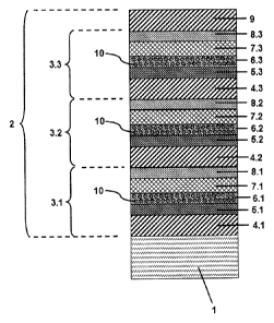
Fig. 1 depicts a cross-section through an embodiment of the transparent pane
according to
the invention with an electrically conductive coating with the transparent
substrate (1) and the
electrically conductive coating (2). The substrate (1) contains float glass
and has a thickness
of 2.1 mm. The electrically conductive coating (2) contains three functional
layers (3),
comprising a first functional layer (3.1), a second functional layer (3.2),
and a third functional
layer (3.3) that are congruently arranged one over another. Each functional
layer (3)
comprises
one layer of an optically highly refractive material (4), respectively
referred to as the
first layer of an optically highly refractive material (4.1), the second layer
of an
optically highly refractive material (4.2), and the third layer of an
optically highly
refractive material (4.3),
- a smoothing layer (5), respectively referred to as the first smoothing
layer (5.1), the
second smoothing layer (5.2), and the third smoothing layer (5.3),
- a lower matching layer (6), respectively referred to as the first lower
matching layer
(6.1), the second lower matching layer (6.2), and the third lower matching
layer (6.3),
a getter material (10) contained in the first lower matching layer (6.1), the
second
lower matching layer (6.2), and the third lower matching layer (6.3),
an electrically conductive layer (7), respectively referred to as the first
electrically
conductive layer (7.1), the second electrically conductive layer (7.2), and
the third
electrically conductive layer (7.3),
an upper matching layer (8), respectively referred to as the first upper
matching layer
(8.1), the second upper matching layer (8.2), and the third upper matching
layer (8.3).
The layers are arranged in the order indicated with increasing distance from
the transparent
substrate (1). A cover layer (9) is arranged above the third functional layer
(3.3). The exact
layer sequence of the functional layers (3.1, 3.2, 3.3) with suitable
materials and exemplary
layer thicknesses is, from the bottom to the top, glass with a thickness of
2.1 mm as the
transparent substrate (1):
- aluminum-doped mixed silicon/zirconium nitride (SiZrNx:A1) as a layer of
an optically
highly refractive material (4) with a thickness of 28 nm (4.1), 59 nm (4.2),
or 60 nm
(4.3),
- antimony-doped mixed tin/zinc oxide (SnZnOx:Sb) with a thickness of 6 nm as
smoothing layers (5),
- titanium-doped zinc/aluminum oxide (ZnO:A1203:Ti) with a thickness of 10 nm
as
lower matching layers (6) with getter material (10),
- silver layer with a thickness of 18 nm as electrically conductive layers
(7),
. CA 02893624 2016-10-20
= 18
- zinc/aluminum oxide (ZnO:A1203) with a thickness of 5 nm as
upper matching layers
(8).
The first functional layer (3.1) is applied directly on the transparent
substrate (1), while the
second functional layer (3.2) is arranged on the first functional layer and
the third functional
layer (3.3) is arranged on the second functional layer (3.2).
The uppermost layer of the electrically conductive coating (2) forms a cover
layer (9) that is
applied on the third functional layer (3.3). The cover layer (9) is made of
aluminum-doped
mixed silicon/zirconium nitride (SiZrNx:A1) with a layer thickness of 40 nm.
The individual layers of the electrically conductive coating (2) were
deposited by cathode ray
sputtering. The target for depositing the lower matching layers (6) contained
95 wt.-% of a
zinc-oxide-based ceramic and 5 wt.-% titanium. The zinc-oxide-based ceramic
contained 98
wt.-% ZnO and 2 wt.-% A1203. The target for depositing the upper matching
layers (8)
consisted of this zinc-oxide-based ceramic containing 98 wt.-% ZnO and 2 wt.-%
A1203. The
deposition of the matching layers (6, 8) was done using cathode sputtering in
the presence of
argon. The target for depositing the smoothing layers (5) contained 68 wt.-%
tin, 30 wt.-%
zinc, and 2 wt.-% antimony. The deposition was done under the addition of
oxygen as
reaction gas during the cathode sputtering. The target for depositing the
layers of an optically
highly refractive material (4) as well as the cover layer (9) contained 52.9
wt.-% silicon, 43.8
wt.-% zirconium, and 3.3 wt.-% aluminum. The deposition was done under
addition of
nitrogen as reaction gas during the cathode sputtering.
Through the design according to the invention of the electrically conductive
coating (2) with
lower matching layers (6) containing a getter material (10), reduced sheet
resistance and,
thus, improved specific heating output compared to the prior art are
advantageously
obtained. The combination of lower matching layer (6) and getter material (10)
makes the
use of an additional blocker layer for protection of the electrically
conductive layer against
oxygen obsolete. Thus, the lower matching layer (6) is in direct contact with
the silver-
containing electrically conductive layer (7), by which means crystalline
growth of the silver is
ensured. This improved crystallinity of the silver results in the desired
reduction of the sheet
resistance of the electrically conductive coating according to the invention.
The optical
properties of the transparent pane according to the invention with an
electrically conductive
coating satisfy the legal requirements for glazings in the automotive sector.
CA 02893624 2016-10-20
19
Fig. 2 and Fig. 3 depict in each case a detail of a transparent pane according
to the invention
with an electrically conductive coating (2) as part of a composite pane. The
composite pane
is intended as a windshield of a passenger car. The transparent substrate (1)
is bonded to a
second pane (11) via a laminating film (16). Fig. 2 depicts a plan view of the
surface of the
transparent substrate (1) facing away from the laminating film (16). The
transparent substrate
(1) is the pane facing the interior of the passenger car. The transparent
substrate (1) and the
second pane (11) contain float glass and have a respective thickness of 2.1
mm. The
laminating film (16) contains polyvinyl butyral (PVB) and has a thickness of
0.76 mm.
An electrically conductive coating (2) is applied on the surface of the
transparent substrate
(1) facing the laminating film (16). The electrically conductive coating (2)
extends over the
entire surface of the transparent substrate (1) minus a circumferential frame-
like coating-free
region with a width b of 8 mm. The coating-free region serves as electrical
insulation
between the voltage-carrying electrically conductive coating (2) and the
vehicle body. The
coating-free region is hermetically sealed by gluing to the laminating film
(16), in order to
protect the electrically conductive coating (2) against damage and corrosion.
One busbar (12) each is arranged on the outer upper and lower edge of the
transparent
substrate (1). The busbars (12) were printed on the electrically conductive
coating (2) using a
conductive silver paste and fired. The layer thickness of the fired silver
paste is 15 pm. The
busbars (12) are electrically conductively connected to the underlying regions
of the
electrically conductive coating (2).
The feed lines (15) are made of tinned copper foils with a width of 10 mm and
a thickness of
0.3 mm. Each feed line (15) is soldered to one of the busbars (12)
respectively. The
electrically conductive coating (2) is connected to a voltage source (13) via
the busbars (12)
and the feed lines (15). The voltage source (13) is the onboard voltage of 14
V of a motor
vehicle.
An opaque ink layer with a width a of 20 mm is applied frame-like on the
second pane (11)
as a masking print (14) on the edge of the surface facing the laminating film
(16). The
masking print (14) conceals from view the strand of adhesive with which the
composite pane
is bonded into the vehicle body. The masking print (14) serves simultaneously
as protection
of the adhesive against UV radiation and thus as protection against premature
aging of the
adhesive. Moreover, the busbars (12) and the feed lines (15) are concealed by
the masking
print (14).
. CA 02893624 2016-10-20
. 20
Fig. 3 depicts a cross-section along A-A' through the composite pane of Fig. 2
in the region
of the lower edge. The transparent substrate (1) with the electrically
conductive coating (2),
the second pane (11), the laminating film (16), a busbar (12), and a feed line
(15) as well as
the masking print (14) are seen.
Fig. 4 depicts a flowchart of the method according to the invention. In a
first step, one layer of
an optically highly refractive material is deposited on a transparent
substrate and, after that,
a smoothing layer is applied thereon. A lower matching layer with a getter
material is
deposited on the smoothing layer, with the getter material being homogeneously
distributed
in the matching layer and being applied in one step therewith. An electrically
conductive layer
is applied on the lower matching layer and an upper matching layer is applied
thereon. This
yields a first functional layer consisting of a layer of an optically highly
refractive material, a
smoothing layer, a lower matching layer with a getter material, an
electrically conductive
layer, and an upper matching layer. At least one second functional layer, at
most four more
functional layers, are applied on this first functional layer. The layer
system is completed by
deposition of a cover layer on the uppermost functional layer. Subsequently,
the layer system
is electrically contacted by installation of a busbar with a feed line. A
laminating film and a
second pane with masking print are laid on the arrangement and the arrangement
is
laminated to produce a composite glass pane.
CA 02893624 2016-10-20
. 21
List of Reference Characters
1 transparent substrate
2 electrically conductive coating
3 functional layer
3.1 first functional layer
3.2 second functional layer
3.3 third functional layer
4 layer of an optically highly refractive material
4.1 first layer of an optically highly refractive
material
4.2 second layer of an optically highly refractive
material
4.3 third layer of an optically highly refractive
material
smoothing layer
5.1 first smoothing layer
5.2 second smoothing layer
5.3 third smoothing layer
6 lower matching layer
6.1 first lower matching layer
6.2 second lower matching layer
6.3 third lower matching layer
7 electrically conductive layer
7.1 first electrically conductive layer
7.2 second electrically conductive layer
7.3 third electrically conductive layer
8 upper matching layer
8.1 first upper matching layer
8.2 second upper matching layer
8.3 third upper matching layer
9 cover layer
getter material
11 second pane
12 busbar
13 voltage source
14 masking print
feed line
16 laminating film
CA 02893624 2016-10-20
=
22
a with of the region masked by the masking print (14)
width of the coating-free region
A-A' section line