Note: Descriptions are shown in the official language in which they were submitted.
CA 02893674 2015-06-03
WO 2014/087356 PCT/1B2013/060648
NETWORK DEVICE
CROSS REFERENCE TO RELA l'ED APPLICATION
[0001] This application claims priority to and all benefits accruing from
United States
Provisional Patent Application 61/733,565 filed in the United States Patent
and
Trademark Office on December 5, 2012.
FIELD OF THE INVENTION
[0002] This invention relates to network devices for connecting to a network,
such as an
Ethernet network. In particular, the invention relates to network devices that
connect to
the network and provide network interconnection.
BACKGROUND
[0003] Network devices provide an important role in receiving and forwarding
data
packets on a network. Depending upon their role in the network, network
devices may be
operative to provide a network support function by receiving and forwarding
data packets
intended for other devices on the network.
[0004] In order to provide for a network device that can be repaired in the
event of a
communications failure, network devices may be provided with modular
input/output
cards that removably engage with a printed circuit board (PCB) of the network
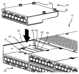
device.
While the removable engagement provides a convenient means to replace a
component of
the network device without having to resort to replacement of the entire
network device,
there is a risk that the engagement functionality provides a potential point
of failure.
[0005] Conventional means for providing modular input/output cards have relied
upon
the use of orthogonal interposer cards that extend from the main device PCB to
provide a
connection plane for the module input/output cards. It has been found that the
additional
connections provide a potential point of mechanical or electrical failure.
Alternative
solutions require specialized connectors that allow the input/output module
PCB to be
- 1 -
CA 02893674 2015-06-03
WO 2014/087356 PCT/1B2013/060648
inserted into the device connector of the device PCB. These specialized
orthogonal
connectors have been found to be more expensive, and potentially create
another point of
mechanical or electrical failure.
[0006] There is a need for an improved modular input/output connection to a
network
device.
SUMMARY
[0007] In an embodiment a network device is provided. The network device
comprising a
mounting rail of the network device having at least one mounting location
defined by one
or more device reference locators, the one or more device reference locators
defining a
mounting location and a mounting direction to the mounting location; the
mounting
location including a device connector attached to a device printed circuit
board (PCB)
and positioned to have a connecting direction parallel to the mounting
direction; a
module for mounting to the mounting location, wherein the module includes
corresponding one or more module reference locators each adapted to engage a
one of the
one or more device reference locators when the module is positioned to be
mounted to
the mounting location, and the module includes a module connector attached to
a module
PCB and positioned to have a connecting direction parallel to the mounting
direction;
wherein the module connector and the device connector are positioned such that
when the
one or more module reference locators are each engaged with the one of the one
or more
device reference locators, and the module is advanced in the mounting
direction towards
the mounting location, the module connector and the device connector connect
as the
module mounts the mounting location to connect the module to the network
device.
[0008] In an implementation of the network device, the device connector is
attached to
the device PCB with a device connecting direction approximately orthogonal to
the
device PCB, wherein the module connector is attached to the module PCB with a
module
connecting direction approximately orthogonal to the surface of the module
PCB, and
wherein the mounting direction is approximately orthogonal to the device PCB
and the
- 2 -
CA 02893674 2015-06-03
WO 2014/087356 PCT/1B2013/060648
module PCB when the one or more module reference locators are each engaged
with the
one of the one or more device reference locators.
[0009] In an implementation, the mounting location comprises a device mounting
surface
and wherein the module has a corresponding device mounting surface, and
wherein when
the module is mounted on the mounting location, the module mounting surface is
in
contact with the device mounting surface.
[0010] In an implementation, a device aperture may be provided through the
device
mounting surface and a module aperture through the module mounting surface.
The
device connector can be located to connect to the module connector through the
device
aperture, and the module connector located to connect to the device connector
through
the module aperture.
[0011] In an implementation, the device connector and the module connector
comprise a
free height connector pair, the free height connector pair having a spacing to
connect the
device connector to the module connector when the module mounting surface is
in
contact with the device mounting surface.
[0012] In an implementation, the module mounting surface and the device
mounting
surface are in sealing engagement when the module is mounted to the mounting
location
[0013] In an implementation, at least one fastener may be provided to secure
the module
to the mounting location, wherein the one or more device reference locators
and the one
or more module reference locators cooperate to position each of the at least
one fastener
relative to a corresponding fastener receiver on the mounting rail.
[0014] In an implementation, the mounting rail further comprises a support
portion
adapted to capture and constrain the device PCB at a location proximate the
device
connector.
[0015] In an implementation, the mounting rail comprises at least a pair of
opposed
mounting locations on opposite sides of the mounting rail. The mounting
direction for
- 3 -
CA 02893674 2015-06-03
WO 2014/087356 PCT/1B2013/060648
each of the pair of opposed mounting locations being towards that side of the
mounting
rail, in opposite directions from one another. A second module may be provided
for
mounting with the module as an opposed pair of modules mounted to the opposite
mounting locations. In an implementation, the device connectors of the opposed
mounting locations are located on opposite sides of the device PCB, such that
when the
opposed pair of modules are mounted to the opposite mounting locations, and
the module
connectors of the opposed pair of modules are connected to the device
connectors of the
opposed mounting locations, the connectors are in opposed alignment.
BRIEF DESCRIPTION OF THE DRAWINGS
[0016] Figures la-fare elevation views of an implementation of a network
device.
[0017] Figure 2 is a partial rear isometric view of an implementation of a
network device.
[0018] Figure 3a illustrates an implementation of a bypass module of a network
device
in a connected state.
[0019] Figure 3b illustrates an implementation of a bypass module of a network
device in
a bypass state.
[0020] Figure 4a is a section view of a module of a network device.
[0021] Figure 4b is a section view of another module of a network device.
[0022] Figure 4c is a section view of a mounting rail of a network device.
[0023] Figure 4d is a section view of the mounting rail and modules in
position for
mounting.
DETAILED DESCRIPTION
[0024] Figures la-f, are elevation views of an exemplary implementation of a
network
device 10. In the implementation of Figures la-if, the network device 10
comprises an
Ethernet switch that provides a plurality of network connections.
- 4 -
CA 02893674 2015-06-03
WO 2014/087356 PCT/1B2013/060648
[0025] Figure la is a top view of the network device 10, comprised of a
chassis 20 that
supports and protects a printed circuit board (PCB) and associated circuit
elements (not
visible in this view). The network device 10 is supplied with power by a pair
of power
supplies, that include heat sinks 12 projecting outside the chassis 20. A
series of cooling
fins 23 assist in dissipating heat generated by the network device 10. A
terminal block 14
provides connections for receiving power to the network device 10. A plurality
of
removable communications modules 30, 32 are also visible in the view.
[0026] Referring to Figure lb, a 'front' view showing a plurality of fiber
optic Ethernet
ports 13 provided by the plurality of removable communications modules 30. In
the
implementation, the modules 30 are shown as opposed pairs of a 'top' module 30
and a
'bottom' module 30. As will be appreciated, use of terms such as 'front',
'top', 'bottom',
and 'rear' are for description purposes with reference to their presentation
in the drawings
only, and are not intended to be limiting for a field installation of the
network device 10.
[0027] The modules 30 may all be of the same size, as illustrated, or may vary
in
dimensions. The modules 30 may all comprise the same networking format, or may
comprise different networking formats. For instance, an additional pair of
removable
modules 32 providing 4 copper Ethernet ports 15 are shown, each of a smaller
size than
one of the modules 30. While the description below refers specifically to the
communications module 30 for clarity, the additional pair of modules 32 can
connect to
the network device 10 in the same manner as the modules 30.
[0028] Figures 1 c and if are side views of the network device 10. Figure ld
is a 'back'
view of the network device 10 showing the heat sinks 12 and a variety of other
input/output connections to the network device 10. Figure le is a bottom view
of the
network device 10 showing the bottom of the terminal block 14, and
communications
modules 30, 32. As mentioned above, the modules 30, 32 shown in Figure le are
each
opposed to a module 30, 32 shown in Figure la.
[0029] Figure 2 is a partial rear isometric view of an exemplary
implementation of a
network device 10. In Figure 2 there are no modules 30 mounted on the mounting
rail 22,
- 5 -
CA 02893674 2015-06-03
WO 2014/087356 PCT/1B2013/060648
but opposed modules 30 are illustrated in position ready for mounting. In the
implementation of Figure 2, a rear portion of the chassis 20 comprises a
mounting rail 22
that provides opposed device mounting surfaces 25 for receiving and supporting
the
plurality of communication modules 30, 32. In an alternate implementation, not
illustrated, the chassis 20 may provide a single device mounting surface 25.
[0030] The chassis 20 is adapted to provide one or more specific mounting
locations on
each of the device mounting surfaces 25 to receive the modules 30. Each of the
modules
30 comprise a complementary module mounting surface 35 adapted to interface
with a
portion of one of the device mounting surfaces 25. Each mounting location
being defined
by one or more device reference locators 40 which are used to interface with
corresponding complementary module reference locators 45 of a module 30 when
mounting the module 30 to the chassis 20.
[0031] In the implementation of Figure 2, two device reference locators 40, in
the form
of guide pins, define a mounting location for each of the modules 30, 32. Each
module
30, 32 has corresponding complementary module reference locators 45 in the
form of
receptacles such as holes or recesses adapted to capture and constrain the
guide pins. As
will be appreciated, the relative locations of the guide pins and the
receptacles may be
reversed such that the device 10 includes receptacles and the module 30
includes guide
pins.
[0032] When the device reference locators 40 are interfaced with the module
reference
locators 45 of a module 30, 32 being mounted on the mounting rail 22, the
mounting
module 30, 32 is constrained to move in a direction perpendicular to the
mounting
surface 25, parallel to a mounting axis of the reference locators 40. The
device reference
locators act to cooperate with the module reference locators 45 to position
the module 30,
32 with reference to the device aperture 62 in the mounting rail 22 that
provides access to
a device connector 60 such as a free height connector. The positioning ensures
alignment
between the device connector 60 and a corresponding module connector 65 on the
module 30, 32 when mounting the module 30, 32 on the mounting rail 22.
- 6 -
CA 02893674 2015-06-03
WO 2014/087356 PCT/1B2013/060648
[0033] While guide pins are illustrated in Figure 2, other implementations of
device
reference locators 40 are contemplated, including features formed into the
chassis with
complementary features formed into the module 30, 32 such as a dovetail.
[0034] In an implementation, the modules 30, 32 are each reversible such that
they may
be mounted to either side of the mounting rail 22 by flipping the module 30
over to orient
the module mounting surface 35 to face one of the device mounting surfaces 25.
In
Figure 2, the two modules 30 are each illustrated with an opposite orientation
to one
another, illustrating the mounting of each module 30 to one of the two opposed
device
mounting surfaces 25 illustrated in Figure 2.
[0035] Fasteners 50, in the form of captive screws in the implementation of
Figure 2, are
provided to secure the module 30, 32 to the mounting rail 22. Corresponding
fastener
receivers 55, in the form of threaded holes in the implementation of Figure 2,
are located
in the mounting rail 22. The device reference locators 40 serve to position
the module 30,
32 on the mounting location to connect with the device connector 60 and to
position the
fasteners 50 in relation to the fastener receivers 55 to provide operative
engagement of
the fasteners 50 with the fastener receivers 55.
[0036] Figures 3a and 3b illustrate the mounting and subsequent removal of a
module 30
from the mounting rail 22. The module 30 of Figures 3a and 3b is at an end
position of
the mounting rail 22, and is shown in relation to the other modules 30 being
mounted to
the mounting rail 22. As illustrated, the load or unload direction of the
module 30 from
the mounting rail 22 is in the same direction as the connection direction of
the device
connector 60 and the module connector 65, such that mounting the module 30 on
the
mounting rail 22 connects the device connector 60 to the module connector 65.
[0037] Figure 4a illustrates a cross-section view of a module 30 oriented for
mounting in
a 'top' position on the mounting rail 22, and Figure 4b illustrates a cross-
section view of a
module 30 oriented for mounting in a 'bottom' position on the mounting rail
22. In each
of the views a daughterboard module PCB 75 is illustrated connected to the
module
connector 65. The module PCB 75 is supported by the chassis of the module 30,
though
- 7 -
CA 02893674 2015-06-03
WO 2014/087356 PCT/1B2013/060648
this connection is not visible in this view. As illustrated, the module
connectors 65 are
each positioned with a connection direction parallel to a pin direction of the
module
connector 65 through the module PCB 75.
[0038] A module aperture 67 in the device mounting surface 35 provides access
to the
module connector 65. An Ethernet port 13 is visible in the view in relation to
the module
connector 65 on the module PCB 75.
[0039] The module aperture 67 and the module connector 65 are positioned
relative to
the module locators 45 to provide for an operative connection with the device
connector
60 when the module 30 is mounted on the mounting rail.
[0040] Figure 4c illustrates a cross-section view of the mounting rail 22. The
device PCB
70 is supported proximate the device connector 60 by a support portion 80 of
the
mounting rail 22.The support portion 80 captures and constrains the device PCB
70 to
position and support the device connectors 60 relative to the device aperture
62 when the
modules 30 are mounted on the mounting rail 22 and the module connectors 65
are
engaged with, and connected to, the device connectors 60. The support portion
80
provides support to the device PCB proximate the device connector 60, to
provide
mechanical support to the device connectors 60. As illustrated, the device
connectors 65
are each positioned with a connection direction parallel to a pin direction of
that device
connector 65 through the device PCB 75. The pin direction being the pins that
extend
from a base of the device connector 65 through the device PCB 75, and form the
mechanical and electrical connection of the device connector 65 to the PCB 75.
[0041] Figure 4d illustrates a cross-section view of the mounting rail 22 of
Figure 4c and
the modules 30 of Figures 4a and 4b in position for mounting to the mounting
rail 22. In
the implementation of Figure 4d, a pair of opposed modules 30 are provided to
mount
and attach to the mounting rail 22 from opposite sides of the mounting rail 22
and to
advance in opposite mountings directions to one another to connect to each of
their
corresponding device connectors 60.
- 8 -
CA 02893674 2015-06-03
WO 2014/087356 PCT/1B2013/060648
[0042] The device reference locators 40 and module reference locators 45, not
visible in
this cross-section view, act to position the modules 30 on the mounting
location such that
when the modules are mounted to the mounting rail 22, the module connectors 65
engage
and connect to the device connectors 60.
[0043] Once secured, the fasteners 50 mechanically attach each module 30 to
the
mounting rail 22, and ensure that the device connector 65 is securely
connected to the
module connector 60. When mounted, the mated mounting surfaces 25, 35 provide
a seal
to seal the device apertures 62 and the module apertures 67 from the
environment. In the
implementation, the opposed modules 30 further provide for opposed mounting
forces
applied to the device PCB 70, resulting in a more stable connection. When the
opposed
pair of modules 30 are mounted to opposing locations on the mounting rail 22,
the
module connectors of the opposed pair of modules are in alignment and
separated by the
device connectors of the opposed mounting locations and the device PCB.
[0044] Accordingly, the mounting forces applied by the fasteners 50 of each of
the
opposed modules 30 applied to the device PCB 70 through the device connectors
60 act
in opposition such that the device PCB 70 is in a slightly compressed state
rather than a
flexed state. Connecting the module connectors 65 to the device connectors 60
presses
the connectors 60, 65 into the corresponding device PCB 70 or module PCB
respectively.
[0045] Furthermore, the insertion forces that arise when connecting the
modules 30 to the
mounting rail 22 act in opposition to one another, and act in parallel to the
pin directions
of the connectors 60, 65. Accordingly, the forces act to press the connectors
60, 65 into
the corresponding PCB 70, 75, rather than as a shear force between the
connector 60, 65
and the PCB 70, 75.
[0046] In the implementation, the device connectors 60 are each attached to an
opposite
side of the device PCB 70 having opposite connection directions approximately
orthogonal to the device PCB. The module connectors 65 are each attached to
one of the
module PCB's 75 with a module connecting direction approximately orthogonal to
that
module PCB 75 . When mounting the modules 30 to the mounting rail 22, the
mounting
- 9 -
CA 02893674 2015-06-03
WO 2014/087356 PCT/1B2013/060648
direction is approximately orthogonal to the device PCB and the module PCB's
75 when
the module reference locators 45 are engaged with their corresponding device
reference
locators 40.
[0047] In an implementation, the device connector 60 and the module connector
65
comprise a pair of free height connectors. The free height connectors selected
to provide
a set-off between the position of the device PCB 70 and the module PCB 75 when
the
module 30 is mounted on the mounting rail 22 and the module mounting surface
35 is
engaged with the device mounting surface 25.
[0048] Various embodiments of the present invention having been thus described
in
detail by way of example, it will be apparent to those skilled in the art that
variations and
modifications can be made without departing from the invention. The invention
includes
all such variations and modifications as fall within the scope of the appended
claims.
- 10-