Note: Descriptions are shown in the official language in which they were submitted.
CA 02894127 2015-05-29
1
SWITCHING STAGE, ENERGY CONVERSION CIRCUIT, AND CONVERSION
STAGE FOR WIND TURBINES COMPRISING THE ENERGY CONVERSION
CIRCUIT
Object of the Invention
The present invention is encompassed in the technical field of electronic
power converters. More specifically, the present invention relates to a
multilevel
energy conversion circuit, especially for being applied in converting energy
from a
wind generator (or wind turbine) and to the switching stage of said conversion
circuit, with a plurality of output voltage levels and large current capacity.
Background of the invention
Electronic converters are widely used in energy generation applications,
such as in wind generators for example. Desired requirements of a converter
include obtaining an output current with the best Total Harmonic Distortion
(THD)
level possible and obtaining a high voltage to minimize conduction losses.
Today, most manufacturers of electronic conversion stages are trying to
increase their power by increasing the number of voltage levels in the output
voltage. Not only does this increase the handled power but it also increases
the
quality of the delivered current by largely reducing the harmonic content.
The two preceding objectives can be achieved by means of using multilevel
converters. These converters are capable of working with different voltage
levels,
to try to obtain an output current with the best THD possible, i.e., with the
best
wave quality possible. They are also capable of increasing the working
voltage,
which is a desirable characteristic for obtaining fewer losses.
A number of multilevel conversion topologies are known in the state of the
art, such as that described in EP0555432A1, EP105179961, EP1673849A1,
EP1815586A1, EP1287609A2 and in "Generalized Multilevel Inverter Topology
with Self Voltage Balancing" by F.Z. Peng, IEEE Transactions on Industry
Applications, Vol. 37, pp. 611 ¨ 618, March/April 2001. Nevertheless, most of
these topologies involve an excessively complicated and expensive
electromechanical design.
For example, the converter described in "Generalized Multilevel Inverter
Topology with Self Voltage Balancing" provides the previously specified
characteristics for a multilevel converter, but it requires a large number of
semiconductors and capacitors, which considerably increases converter size and
CA 02894127 2015-05-29
1
2
cost.
Another multilevel converter providing the aforementioned characteristics is
that described in EP0555432A1, which consists of n cells, made up of one
capacitor and two semiconductors, series-connected one after the other. The
increase in the available voltage levels is done by means of adding or taking
away
the capacitor voltages. However, this converter has the drawback of being
large-
sized and expensive due to the capacitors, which largely complicates the
electromechanical design. The need for this large size limits the number of
levels
that can be reached by this converter because there comes a time when the
required volume makes it no longer viable.
EP1287609A2 proposes a converter that allows reducing capacitor volume.
Like in the converter disclosed in EP0555432A1 described above, the converter
proposed in EP1287609A2 consists of cells series-connected, but in this case,
each cell consists of two capacitors and three pairs of semiconductors. This
enables achieving three voltage levels with each cell and, in the case of
series-
connecting n cells, 2*n+1 levels in total. The problem with cells of this type
is that
two pairs of semiconductors are arranged in series, which complicates control
over
distributing voltage among them.
EP1051799B1 proposes a multilevel converter called Active Neutral Point
Clamped (ANPC) converter, consisting of a Neutral Point Clamped (NPC) type
converter in which the level or clamp diodes are replaced with controlled
semiconductors. On the other hand, if more than three output voltage levels
are
desired, it proposes intercalating capacitors in the output stage. The main
problem
with the converter described in EP1051799B1 is that to obtain a converter of n
levels it is necessary to series-connect (n-1)/2 controlled semiconductors,
complicating the distribution of voltages among said semiconductors.
EP1673849A1 attempts to solve this problem, disclosing a multilevel
converter formed by series-connecting several switching units, each of which
is
made up of two controlled semiconductors arranged in series through a
capacitor.
A problem shared by all the mentioned converters is the overvoltages
occurring in the semiconductors in switching. These overvoltages are caused by
stray inductances and in practice they reduce the current capacity and the
service
life of the semiconductors. The circuit described in EP1815586A1, using
additional
voltage limiting circuits and semiconductors, tries to mitigate this
phenomenon, but
these additional elements increase cost and size and make the converter more
CA 02894127 2015-05-29
3
complex.
Therefore the technical problem is to be able to convert energy by obtaining
an output voltage and current which minimize conduction losses without
increasing
the size, complexity or cost of the converter.
Description of the Invention
The present invention serves to solve the aforementioned problem by
means of a switching stage that can be integrated in an energy conversion
circuit
which reduces the number and/or size of the required capacitors, fixes the
voltage
of the switches, reduces the overvoltages experienced by switches in
switching,
providing a multilevel energy converter, with n output voltage levels, both
for direct
current to alternating current (DC/AC) conversion and alternating current to
direct
current (AC/DC) conversion, having considerable advantages with respect to the
converters of the prior state of the art because of its smaller size and lower
cost,
greater design simplicity, greater operating and control simplicity, and
improved
attainable power levels.
The present invention can be applied in wind generator systems, among
other energy conversion systems.
One aspect of the invention relates to a switching stage with n output
voltage levels, which can be integrated in an energy conversion circuit,
consisting
of a bus with a plurality of m capacitors, interconnected between a positive
bus
voltage terminal and a negative bus voltage terminal, having m-1 intermediate
bus
voltage terminals between the previous two positive and negative bus voltage
terminals. This switching stage comprises multiple linked cells, each
consisting of
m+1 input terminals, m+1 output terminals and at least one capacitor connected
to
any two of the m+1 output terminals, and m+1 switches, each switch i (i=1,
m,
m+1) being connected between the input terminal i and the output terminal i of
the
cell. The connection between the p (p>=1) cells of the switching stage is as
follows:
- connecting, for j=1 to j=p-1, cell j to cell j+1 such that:
- for i=1 to i=m+1, output terminal i of cell j is connected to input
terminal i of cell j+1,
- connecting cell 1 to m DC bus capacitors as follows:
- for i=1 to i=m+1, input terminal i of cell 1 is connected to bus
voltage terminal i.
The proposed switching stage has a total of m+1 output terminals,
CA 02894127 2015-05-29
4
consisting of the positive output terminal of the switching stage, m-1
intermediate
output terminals and the negative output terminal of the switching stage, and
having output terminal i of the switching stage connected to output terminal i
of cell
p, for 1=1 (corresponding to the positive output terminal) to i=m+1
(corresponding
to the negative output terminal of the switching stage).
In a preferred embodiment, the number of intermediate terminals is equal to
1, i.e., the number of bus capacitors is equal to 2. Two possible embodiments
of
the switching stage can be distinguished from this configuration. In a
possible
embodiment of the invention, a capacitor is connected between the positive
output
terminal and intermediate output terminal, and between the intermediate output
terminal and negative output terminal in all the cells of the switching stage.
This
embodiment allows reducing the overvoltages experienced by all the switches
during switching and fixing the voltage of all the semiconductors. In another
possible embodiment, a capacitor is connected between the positive output
terminal and intermediate output terminal, and between the intermediate output
terminal and negative output terminal in some of the cells of the switching
stage,
while only one capacitor is connected between the positive output terminal and
negative output terminal of other cells. This last preferred embodiment allows
reducing the overvoltage experienced by many of the switches during switching,
fixing the voltage of the switches and distributing the losses of some of the
switches.
The bus can also preferably consist of 3 or 4 capacitors, i.e., the number of
intermediate voltage terminals of the cells is 2 or 3, respectively. In both
cases,
preferably all the cells of the switching stage connect to each capacitor
between
every two adjacent terminals of all the cells, such that the voltage of the
switches
is fixed and the overvoltages experienced by the switches during switching are
reduced compared with other converters.
According to a possible embodiment of the invention, optionally some of the
capacitors of the switching stage can have a series-connected resistor to
limit
voltage and current oscillations during switching.
The capacitors of the cells of the switching stage, proposed as a switching
stage which can be part of an energy converter, solve the problem of the
overvoltages experienced in the semiconductors of some converters of the state
of
the art, such as those described in the previously cited documents
EP1287609A2,
EP105179961, EP1673849A1 and EP1815586A1, because said capacitors of the
CA 02894127 2015-05-29
cells provide paths for the current with lower inductance than in the
mentioned
converters.
The switches of the switching stage can be IGBTs (Isolated Gate Bipolar
Transistor), IGCTs (Integrated Gate Controlled Thyristor), IEGTs (Injection
5
Enhanced Gate Transistor), GTO (Gate Turn-Off) thyristors and any combination
thereof, anti-parallel connecting a diode for any of them, thereby obtaining
two-
way semiconductors with respect to current and one-way semiconductors with
respect to voltage.
The switches of the switching stage can be controlled by means of a pulse
width modulation (PWM) strategy which allows synthesizing an alternating
voltage
in the AC terminal.
Another aspect of the invention relates to a DC/AC or AC/DC energy
conversion circuit for n output voltage levels, comprising the switching stage
described above (with its plurality of cells, each cell consisting of m+1
switches
and at least one capacitor, the m+1 output terminals of each cell, including
one
positive voltage terminal, another negative voltage terminal and m-1
intermediate
voltage terminals in each linked cell), and further comprising a multilevel
converter
with m+1 voltage terminals, including one positive voltage terminal, another
negative voltage terminal and m-1 intermediate voltage terminals, which are
connected respectively to the output terminals of the switching stage.
When comparing the conversion circuit of the invention with those already
existing and discussed in the state of the art, such as the converter
described in
the previously cited document "Generalized Multilevel Inverter Topology with
Self
Voltage Balancing" by F.Z. Peng, the conversion circuit herein proposed
requires a
smaller number of semiconductors and the capacitors are smaller in size. The
proposed circuit also has this advantage of requiring a smaller size for the
capacitors compared with the converter described in EP0555432A1. The present
circuit further has the advantage of assuring semiconductor voltage
distribution
compared with the converters described in EP1287609A2 and EP1051799B1.
The energy conversion circuit of the present invention has redundant
switching states, i.e., the same output voltage level is obtained with
different
semiconductor switching states. However, these redundant switching states have
a contrary effect on capacitor voltage. To that end, the capacitor voltage can
be
controlled by using redundant switching states.
The energy conversion circuit according to the present invention can
CA 02894127 2015-05-29
6
preferably be integrated in a three-phase system, where at least one
conversion
circuit according to the invention can be connected for each phase. Another
possible implementation option is for the energy conversion circuit to be
integrated
in a configuration where at least two three-phase converters share the same DC
bus (Back-To-Back configuration), connecting an energy conversion circuit
according to the invention on the power grid side and another energy
conversion
circuit according to the invention on the energy generator side.
To keep the voltage of the intermediate DC voltage terminals in the three-
phase system to which a conversion circuit according to the invention is
connected
in each electric phase stable, additional voltage control and/or modulation
control
hardware is required. For example, for the case of a bus with two capacitors
in the
switching stage of the conversion circuit, the voltage of the intermediate DC
voltage terminal can be controlled by means of the homopolar voltage, i.e., by
using different phase voltages providing equal line voltages and having a
different
effect on the voltage of the intermediate DC voltage terminal, as shown in "A
Comprehensive Study of Neutral-Point Voltage Balancing Problem in Three-Level
Neutral-Point-Clamped Voltage Source PWM Inverters" by N. Celanovic, IEEE
Transactions on Power Electronics, Vol. 15, pp. 242-249, March 2000. For the
case of 2 or 3 intermediate DC voltage terminals, a Back-To-Back configuration
(two three-phase converters share the same DC bus) is preferred because in
this
configuration, there are techniques for controlling the voltage of said
terminals,
such as that shown in "An Optimal Controller for Voltage Balance and Power
Losses Reduction in MPC AC/DC/AC Converters" by M. Marchesoni, IEEE 31st
Annual Power Electronics Specialists Conference, Vol. 2, pp., 662-667, 2000.
The energy conversion circuit can particularly be applied in wind generator
systems and can be integrated in wind turbine conversion stages, so another
aspect of the present invention is an energy conversion stage for wind
turbines
comprising a circuit such as that described above.
Description of the Drawings
To complement the description that is being made and for the purpose of
aiding to better understand the features of the invention according to a
preferred
practical embodiment thereof, a set of drawings is attached as an integral
part of
said description wherein the following has been depicted with an illustrative
and
non-limiting character:
Figure 1 shows a schematic depiction of a controlled semiconductor
CA 02894127 2015-05-29
7
example of the semiconductor type used in the present invention;
Figure 2A shows a switching stage according to a possible embodiment of
the invention for an example with 3 output voltage terminals and a capacitor
connected between every two adjacent terminals in each cell of the stage.
Figure 2B shows a switching stage according to a possible embodiment of
the invention for an example with 3 butput voltage terminals with a capacitor
between every two adjacent terminals in some of the cells and a single
capacitor
between the positive and negative terminals of some of the cells of the stage.
Figure 20 shows a switching stage according to a possible embodiment of
the invention for an example with 4 output voltage terminals and three cells.
Figure 2D shows a switching stage according to a possible embodiment of
the invention for an example with 4 output voltage terminals and four cells.
Figure 3A shows a conversion circuit with a switching stage according to a
possible embodiment of the invention for an example with 5 output voltage
levels
and two cells in the switching stage connected to an NPC converter with clamp
diodes.
Figure 3B shows a conversion circuit with a switching stage according to
another possible embodiment of the invention for an example with 5 output
voltage
levels and two cells in the switching stage, replacing the clamp diodes with
controlled semiconductors.
Figure 3C shows a conversion circuit with a switching stage according to a
possible embodiment of the invention for an example with 5 output voltage
levels
and two cells in the switching stage, with a Generalized Multilevel Inverter
connected to the stage.
Figure 4A shows a conversion circuit with a switching stage according to a
possible embodiment of the invention for an example with 7 output voltage
levels
and four cells in the switching stage, connected to an NPC converter.
Figure 4B shows a conversion circuit with a switching stage according to a
possible embodiment of the invention for an example with 7 output voltage
levels
and four cells in the switching stage, connected to a Generalized Multilevel
Inverter.
Figure 40 shows a conversion circuit with a switching stage according to a
possible embodiment of the invention for an example with 7 output voltage
levels
and two cells in the switching stage.
Figure 5 shows a conversion circuit with a switching stage according to a
CA 02894127 2015-05-29
8
possible embodiment of the invention for an example with 7 output voltage
levels
and three cells in the switching stage.
Figure 6A shows a conversion circuit with a switching stage according to a
possible embodiment of the invention for an example with 9 output voltage
levels
and four cells in the switching stage, with a DCC converter.
Figure 6B shows a conversion circuit with a switching stage according to a
possible embodiment of the invention for an example with 9 output voltage
levels
and four cells in the switching stage, with an MPC converter.
Figure 7 a switching stage according to a possible embodiment of the
invention for an example with four cells, two bus capacitors and some
capacitors
with a series-connected resistor.
Preferred Embodiment of the Invention
The invention is described below in reference to the different figures which
depict, in the case of Figures 2A, 2B, 2C 2D and 7, several implementation
examples of a switching stage according to the present invention which can be
applied in a multilevel conversion circuit, whereas Figures 3A, 3B, 3C, 4A,
4B, 4C,
5 and 6A-6B illustrate different embodiments of the multilevel conversion
circuit
with a switching stage according to the invention. In the embodiments herein
illustrated, controlled semiconductors, for example, an IGBT, i.e., an
Insulated
Gate Bipolar Transistor, such as those shown in Figure 1, are used as
switches. In
any case, the drawings and examples do not intend to limit the invention to
any
specific embodiments.
Reference numbers identifying the following elements are shown in the
drawings:
(1) positive DC voltage terminal
(2) intermediate DC voltage terminal
(3) negative DC voltage terminal
(4) AC voltage terminal
(5) DC bus capacitor
(6) positive output terminal of the switching stage
(7) intermediate output terminal of the switching stage
(8) negative output terminal of the switching stage
(9) switch
(10) capacitor
(11) resistor
CA 02894127 2015-05-29
9
(12) positive voltage terminal of the multilevel converter
(13) intermediate voltage terminal of the multilevel converter
(14) negative voltage terminal of the multilevel converter
(C) collector
(E) emitter
(P) gate
(D) diode
Figure 1 shows a conventional controlled IGBT semiconductor, comprising
a collector (C), a gate (P), an emitter (E) and a diode (D), which can perform
the
function of a switch (9) in the different embodiments of the multilevel energy
conversion circuit proposed below. The switches (9) can be two-way with
respect
to current and one-way with respect to voltage.
Figures 2A, 26, 2C and 2D show various implementation examples of a
multilevel switching stage according to the invention, comprising a plurality
of
controlled IGBT semiconductors acting as switches (9) and a bus of capacitors,
for
the cases of a configuration with 2, 3 or 4 DC bus capacitors (5), i.e., for
1, 2 or 3
intermediate DC voltage terminals (2).
Figure 2A shows an example of a switching stage (210) with p = 4 cells
(211, 212, 213, 214) and for the case of having 2 bus capacitors (5) with m=2,
i.e.,
m-1 = 1 intermediate DC voltage terminal (2), connecting one capacitor (10)
between every two adjacent terminals of each cell.
Figure 2B shows an example also for the case of 2 bus capacitors (5) in a
switching stage (220) having p= 4 cells (221, 222, 223, 224) and connecting
one
capacitor (10) between every two adjacent terminals of some of the cells, but
connecting only one capacitor (10) between the positive and negative terminals
(6,
8) of some of the cells (222, 224).
Figure 20 shows an example for the case of 3 bus capacitors (5) in a
switching stage (230) having 3 cells (231, 232, 233), with m=3, i.e., m-1 = 2
intermediate DC voltage terminals (2), and connecting one capacitor (10)
between
every two adjacent terminals of each cell.
Figure 2D shows an example for the case of 4 bus capacitors (5) in a
switching stage (240) having p = 4 cells (241, 242, 243, 244) and m=4, i.e., m-
1 =
3 intermediate DC voltage terminals (2), connecting one capacitor (10) between
every two adjacent terminals of each cell.
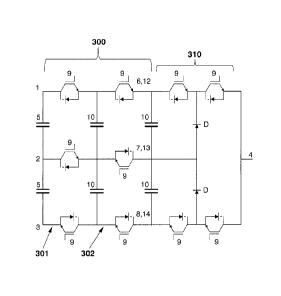
Figures 3A, 3B and 30 show three possible embodiments of the invention
CA 02894127 2015-05-29
for the case of an energy conversion circuit with n=5 voltage levels,
comprising a
switching stage (300) having p = 2 cells (301, 302) and a bus of capacitors
made
up of 2 capacitors (5) in the three examples. What distinguishes one
embodiment
of the invention from another in this case is the multilevel converter which
is
5
connected to the switching stage (300) of the energy conversion circuit. In
Figure
3A, a multilevel Neutral Point Clamped (NPC) converter (310) is connected to
the
switching stage (300); in Figure 3B, a multilevel Active Neutral Point Clamped
(ANPC) converter (320) is connected; and in Figure 3C, the switching stage
(300)
is connected to a Generalized Multilevel Inverter converter (330) such as that
10
described by F.Z. Peng in "Generalized Multilevel Inverter Topology with Self
Voltage Balancing", IEEE Transactions on Industry Applications, 2001,
mentioned
in the prior state of the art. Generally, for this configuration case of the
circuit with
5 voltage levels and two cells (301, 302) linked in the switching stage, the
multilevel converter which can be connected to the switching stage (300) can
be
any converter having 3 terminals, i.e., its bus is made up of 2 capacitors.
Other possible embodiments of the energy conversion circuit which is
described for the case m=2 comprises the proposed switching stage connected to
a multilevel Transistor Clamped Converter (TCC) or to a multilevel Stacked
Multi-
Cell (SMC) converter.
Figures 4A, 4B and 4C show three possible embodiments of the invention
for the case of an energy conversion circuit with n=7 voltage levels,
comprising a
switching stage with a bus of capacitors made up of 2 capacitors (5) in the
three
examples. Two preferred configurations can be distinguished within this
converter
configuration with 7 levels and bus of 2 capacitors: in one configuration, the
switching stage is made up of 4 cells and in the other configuration the
switching
stage is made up of 2 cells.
Figure 4A shows an embodiment in which the switching stage (410) is
made up of 4 cells (411, 412, 413, 414) and two DC bus capacitors (5), one
connected between the positive DC voltage terminal (1) and an intermediate DC
voltage terminal (2) and the other connected between the latter and the
negative
DC voltage terminal (3). The switching stage (410) is connected to a
multilevel
NPC converter (415), i.e., neutral point clamped converter, which has an AC
voltage terminal (4) for connecting to the power generating machine, for
example,
a wind turbine.
Figure 4B shows another embodiment of an energy conversion circuit with 7
CA 02894127 2015-05-29
11
voltage levels, where the switching stage (420) is also made up of 4 cells
(421,
422, 423, 424) and two DC bus capacitors (5), but a Generalized Multilevel
Inverter (425) such as that described by F.Z. Peng in the aforementioned
background document of the prior state of the art is connected to said
switching
stage (420).
Another embodiment option can be connecting the switching stage (410,
420) having 4 cells to an ANPC converter, i.e., Active Neutral Point Clamped
Converter.
Figure 4C shows an embodiment of an energy conversion circuit with 7
voltage levels and also a switching stage (430) with two DC bus capacitors (5)
but
where said switching stage (430) is made up of only 2 cells (431, 432) and
connected to it there is a multilevel converter with multiple series-connected
switching groups (435), which can be a 5L-ANPC converter having 5 active
neutral
point clamped levels such as that described according to the previously
mentioned
patent application EP1673849A1, which in the illustrated example comprises two
first switching groups (4351, 4352) parallel-connected to one another and in
turn
parallel-connected to a second switching group (4353) and a third switching
group
(4354), each switching group made up of a first and a second controlled
semiconductor (9) which are series-conriected through a capacitor (10).
In all cases, the positive output terminal (6) of the switching stage is
connected to the positive voltage terminal (12) of the multilevel converter
and the
negative output terminal (8) of the switching stage is connected to the
negative
voltage terminal (14) of the multilevel converter. Furthermore, the switching
stage
has a single intermediate output terminal (7), i.e., m=2, connected to an
intermediate voltage terminal of the multilevel converter (13),
Figure 5 shows a preferred embodiment of the invention of an energy
conversion circuit also with 7 voltage levels for the case of a switching
stage (510)
consisting of 3 DC bus capacitors (5) and 3 cells (511, 512, 513), having two
intermediate output terminals of the switching stage (7) which are connected
respectively to respective intermediate voltage terminals of the converter
(13), i.e.,
m = 3. The multilevel converter which is connected to the switching stage
(510)
can be any converter having 4 terminals, i.e., its bus is made up of 3
capacitors,
for example, a Neutral Point Clamped (NPC) converter, a Diode Clamped
Converter (DCC), a Generalized Multilevel Inverter, etc. In the example of
Figure
5, the switching stage (510) is connected to a Diode (D) Clamped Converter
=
CA 02894127 2015-05-29
12
(DCC) (515).
Figures 6A and 6B show two preferred embodiments of the invention for the
case of an energy conversion circuit having n = 9 voltage levels with a
switching
stage (600) consisting of 4 DC bus capacitors (5) and 4 cells (601, 602, 603,
604),
having three intermediate output terminals of the switching stage (7) which
are
connected respectively to intermediate voltage terminals of the multilevel
converter
(13), i.e., m = 4. The multilevel converter which is connected to the
switching stage
(600) can be any converter having 5 terminals, i.e., its bus is made up of 4
capacitors, for example, an NPC, a DCC, a Generalized Multilevel Inverter, a
Multi
Point Clamped (MPC) converter, etc. For example, in Figure 6A, the switching
stage (600) is connected to a multilevel DCC converter (615), whereas in
Figure
6B, the switching stage (600) is connected to a multilevel MPC converter
(625).
Figure 7 shows a preferred embodiment of the invention for the case of a
switching stage (700) with p=4 cells (701, 702, 703, 704), and two DC bus
capacitors (5), having a single intermediate output terminal (7), i.e., m=2,
consisting of capacitors (10) series-connected to resistors (11) to limit
voltage and
current oscillations in the semiconductors (9) during switching.
Note that in this text the term "comprises" and its derivatives (such as
"comprising", etc.) must not be understood in an excluding sense, i.e., these
terms
must not be interpreted so as to exclude the possibility that what is
described and
defined above can include additional elements, stages, etc.