Note: Descriptions are shown in the official language in which they were submitted.
METHOD AND APPARATUS FOR ANALYTE MEASUREMENT
[0001]
[0002]
FIELD
[0003] The present disclosure generally relates to methods and systems for
analyte
measurement.
BACKGROUND
[0004] Fig. 1 shows a specimen test strip 100 with a reaction area 102.
Reaction
area 102 contains reagents that react with an analyte in a specimen sample,
such
as glucose in a blood sample. When the specimen sample reaches reaction area
102, reaction area 102 changes color according to a characteristic of the
analyte,
such as the glucose level in blood. The user visually compares the color of
reaction
area 102 against a chart 104 to correlate the color of reaction area 102 to
the
characteristic of the analyte. Alternatively the user inserts specimen test
strip 100
into a meter, which optically determines the characteristic of the analyte.
SUMMARY
[0005] According to aspects of the present disclosure, a method is provided
for a
portable computing device to read a reaction area on a test strip, which is
located in
a test strip peripheral device placed over an image sensor and a light source
of the
portable computing device. Light is provided with the light source, which the
peripheral device directs to the reaction area. An image including the
reaction area
is captured with the image sensor. An analyte characteristic is determined
based on
a color of the captured reaction area in the image.
CA 2894421 2018-11-09
CA 02894421 2015-06-09
WO 2014/094442 2 PCT/CN2013/081138
[0006] According to other aspects of the present disclosure, a test strip
peripheral
device is to be placed over an image sensor and a light source of a portable
computing device to assist the portable computing device in reading a reaction
area
on a test strip in the peripheral device. The peripheral device includes a
light guide
to direct light from the light source to the test strip, and an alignment
feature to aid
the placement of the peripheral device relative to the image sensor and the
light
source on the portable computing device.
[0007] According to other aspects of the present disclosure, a test strip is
to detect
an analyte characteristic in a specimen sample. The test strip includes a
reaction
area to receive the specimen sample, and conductive smart dots to be detected
by a
touchscreen. Information about the test strip is conveyed based on an
arrangement
of the smart dots, an orientation of the smart dots, or both.
BRIEF DESCRIPTION OF THE DRAWINGS
[0008] The foregoing and other features of the present disclosure will become
more
fully apparent from the following description and appended claims, taken in
conjunction with the accompanying drawings. Understanding that these drawings
depict only several embodiments in accordance with the disclosure and are
therefore not to be considered limiting of its scope, the disclosure will be
described
with additional specificity and detail through use of the accompanying
drawings.
[0009] In the drawings:
[0010] Fig. 1 shows a prior art specimen test strip;
[0011] Figs. 2A and 2B show systems each including a portable computing device
and a test strip peripheral device to assist the portable computing device in
reading
a test strip in examples of the present disclosure;
[0012] Fig. 3 shows a side view of a first test strip peripheral device for
portable
computing devices in examples of the present disclosure;
CA 02894421 2015-06-09
WO 2014/094442 3
PCT/CN2013/081138
[0013] Fig. 4 shows a side view of a second test strip peripheral device for
portable
computing devices in examples of the present disclosure;
[0014] Fig. 5 shows a side view of a third test strip peripheral device for
portable
computing devices in examples of the present disclosure;
[0015] Fig. 6 shows a side view of a fourth test strip peripheral device for
portable
computing devices in examples of the present disclosure;
[0016] Fig. 7 shows a side view of a fifth test strip peripheral device for
portable
computing devices in examples of the present disclosure;
[0017] Figs. 8A and 8B show side and top views of a sixth test strip
peripheral
device for portable computing devices in examples of the present disclosure;
[0018] Fig. 9 shows the screen of a portable computing device with an
alignment
mark to facilitate the placement of a test strip peripheral device in examples
of the
present disclosure;
[0019] Figs. 10A, 10B, and 10C show test strips with reaction and reference
areas in
examples of the present disclosure;
[0020] Figs. 11A, 11B, and 11C show test strips with reaction and color
calibration
areas in examples of the present disclosure;
[0021] Fig. 12A shows conductive smart dots on a test strip or a test strip
peripheral
device in examples of the present disclosure;
[0022] Figs. 12B, 12C, 12D, and 12E show different types of smart dots in
examples
of the present disclosure;
[0023] Figs. 13A, 13B, and 13C show different arrangements of smart dots in
examples of the present disclosure;
[0024] Fig. 14A shows a test strip with a reaction area and a temperature
sensor in
examples of the present disclosure;
CA 02894421 2015-06-09
WO 2014/094442 4 PCT/CN2013/081138
[0025] Fig. 14B shows a test strip with reaction and temperature indication
areas in
examples of the present disclosure;
[0026] Fig. 15 shows a seventh test strip peripheral device for portable
computing
devices in examples of the present disclosure;
[0027] Fig. 16 shows an eighth test strip peripheral device for portable
computing
devices in examples of the present disclosure;
[0028] Figs. 17A, 17B, 17C, and 17D show perspective, top bottom, and side
views
of a ninth test strip peripheral device in examples of the present disclosure;
[0029] Fig. 18 shows the screen of a portable computing device in examples of
the
present disclosure;
[0030] Fig. 19 is a flowchart of a method for a portable computing device to
read a
test strip in a test strip peripheral device placed on the portable computing
device in
examples of the present disclosure;
[0031] Fig. 20 shows the screen of a portable computing device in examples of
the
present disclosure; and
[0032] Figs. 21A, 21B, 21C, and 21D show first perspective, second
perspective,
top, and side views of a tenth test strip peripheral device in examples of the
present
disclosure.
DETAILED DESCRIPTION
[0033] As used herein, the term "includes" means includes but not limited to,
the
term "including" means including but not limited to. The terms "a" and "an"
are
intended to denote at least one of a particular element. The term "based on"
means
based at least in part on.
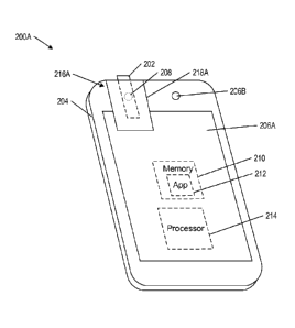
[0034] Fig. 2A shows a system 200A to detect a characteristic of an analyte on
a test
strip 202 in examples of the present disclosure. System 200A includes a
portable
computing device 204, such as a smart phone or a tablet computer. Device 204
has
CA 02894421 2015-06-09
WO 2014/094442 5
PCT/CN2013/081138
a screen 206A (e.g., a touchscreen), a flash 206B, an image sensor 208 (shown
in
phantom), a non-transitory computer readable medium 210 (shown in phantom) for
storing processor executable instructions of an application 212 (shown in
phantom),
and a processor 214 (shown in phantom) to run the application. Executing
application 212, processor 214 illuminates a reaction area on test strip 202
with light
from screen 206A, captures an image of the reaction area with image sensor
208,
determines the color of the captured reaction area in the image, and
determines the
analyte characteristic based on the color of the captured reaction area in the
image.
[0035] System 200A includes a test strip peripheral device 216A that assists
device
204 in reading the reaction area on test strip 202. Peripheral device 216A
includes
a light guide 218A that directs light from screen 206A to the reaction area on
test
strip 202.
[0036] Fig. 2B shows a system 200B to detect a characteristic of an analyte on
test
strip 202 in examples of the present disclosure. System 200B includes device
204
and a test strip peripheral device 216B. Executing application 212, processor
214
illuminates the reaction area on test strip 202 with light from flash 206B
(shown in
phantom), captures an image of the reaction area with image sensor 208,
determines the color of the captured reaction area in the image, and
determines the
analyte characteristic based on the color of the captured reaction area in the
image.
[0037] Peripheral device 216B includes a light guide 218B that directs light
from
flash 206B to the reaction area on test strip 202. Peripheral device 216B
includes a
color filter 220 (shown in phantom) to control the color of the light
illuminating the
reaction area on test strip 202.
[0038] Fig. 3 shows a test strip peripheral device 300 for device 204 in
examples of
the present disclosure. Peripheral device 300 includes a test strip slot or
compartment 302 to receive test strip 202, a light guide 304 to direct light
from a
light source, such as screen 206A or flash 206B, to the reaction area on the
test
strip, and an alignment feature 306 to aid the placement of the peripheral
device on
the portable computing device. When flash 206B is used as the light source,
CA 02894421 2015-06-09
WO 2014/094442 6
PCT/CN2013/081138
peripheral device 300 includes a color filter 308 to control the color of the
light
illuminating the reaction area on test strip 202.
[0039] Light emits upward from screen 206A or flash 206B, optionally travels
through
color filter 308, reflects diagonally downward from a reflective surface 310
of light
guide 304, passes through the reaction area on test strip 202, and impinges
image
sensor 208.
[0040] In some examples, light guide 304 is a transparent block and reflective
surface 310 is a beveled edge of the transparent block that reflects light by
total
internal reflection (TIR) or a reflective coating. Light guide 304 may be
covered in a
case or by a coating to prevent ambient light from entering so the reaction
area on
test strip 202 is illuminated substantially by screen 206A or flash 206B. In
other
examples light guide 304 is the reflective interior in a hollow case of
peripheral
device 300 and reflective surface 310 is a surface of the reflective interior.
The
hollow case blocks ambient light so the reaction area on test strip 202 is
illuminated
substantially by screen 206A or flash 206B.
[0041] Color filter 308 is located above a portion of screen 206A or flash
206B. In
other examples color filter 308 is located over test strip 202.
[0042] Alignment feature 306 abuts against an edge 312 of device 204 to place
test
strip 202 above imaging sensor 208 and reflective surface 310 of light guide
304
over a portion of screen 206A or flash 206B. In other examples, alignment
feature
306 may be received in an opening on device 204, such as a speaker opening or
an
earphone jack.
[0043] Fig. 4 shows a test strip peripheral device 400 for device 204 in
examples of
the present disclosure. Peripheral device 400 includes a test strip slot or
compartment 402 to receive test strip 202, a light guide 404 to direct light
from
screen 206A or flash 206B to the reaction area on the test strip, and an
alignment
feature 406 to aid the placement of the peripheral device on the portable
computing
device. When flash 206B is used as the light source, peripheral device 400
includes
CA 02894421 2015-06-09
WO 2014/094442 7
PCT/CN2013/081138
a color filter 408 to control the color of the light illuminating the reaction
area on test
strip 202.
[0044] Light emits from screen 206A or flash 206B, optionally travels through
color
filter 408, travels from an entrance face 412 of light guide 404 to an exit
face 414 of
the light guide, reflects diagonally downward from the reaction area on test
strip 202,
and impinges image sensor 208.
[0045] Light guide 404 is slanted so entrance face 412 is located above a
portion of
screen 206A or flash 208 and exit face 414 is located below the reaction area
on
test strip 202. In some examples, light guide 404 is a transparent block that
constrains light by TIR or a reflective coating on its surfaces. In other
embodiments,
light guide 404 is hollow and constrains light by a reflective coating on its
surfaces.
Light guide 404 may be covered in a case or by a coating to prevent ambient
light
from entering so the reaction area on test strip 202 is illuminated
substantially by
screen 206A or flash 206B.
[0046] Color filter 408 is located above a portion of screen 206A or flash
206B. In
other examples color filter 408 is located below the reaction area on test
strip 202.
[0047] Alignment feature 406 abuts against edge 312 of device 204 to place
test
strip 202 above imaging sensor 208 and light guide 404 over a portion of
screen
206A or flash 206B. In other examples, alignment feature 406 may be received
in
an opening on device 204, such as a speaker opening or an earphone jack.
[0048] Fig. 5 shows a test strip peripheral device 500 for device 204 in
examples of
the present disclosure. Peripheral device 500 includes a test strip slot or
compartment 502 to receive test strip 202, a light guide 504 to direct light
to and
from the reaction area to imaging sensor 208, and an alignment feature 506 to
aid
the placement of the peripheral device on the portable computing device. When
flash 206B is used as the light source, peripheral device 500 includes a color
filter
508 to control the color of the light illuminating the reaction area on test
strip 202.
CA 02894421 2015-06-09
WO 2014/094442 8
PCT/CN2013/081138
[0049] In some examples, light emits upward from screen 206A or flash 206B,
optionally travels through color filter 508, reflects diagonally downward from
a first
reflective surface 510 of light guide 504, reflects diagonally upward from the
reaction
area on test strip 202, reflects downward from a second reflective surface 512
of the
light guide, and impinges image sensor 208.
[0050] In some examples, light guide 504 is a transparent block, first
reflective
surface 510 is a beveled edge of the transparent block that reflects light by
TIR or a
reflective coating, and second reflective surface 512 is a reflector embedded
in the
light guide. Light guide 504 may be covered in a case or by a coating to
prevent
ambient light from entering so the reaction area on test strip 202 is
illuminated
substantially by screen 206A or flash 2066. In other examples light guide 504
is the
reflective interior in a hollow case of peripheral device 500 and reflective
surfaces
510, 512 are surfaces of the reflective interior. The hollow case blocks
ambient light
so the reaction area on test strip 202 is illuminated substantially by screen
206A or
flash 2066.
[0051] Color filter 508 is located above a portion of screen 206A or flash
206B. In
other examples color filter 508 is located over test strip 202.
[0052] Alignment feature 506 abuts against edge 312 of device 204 to place
second
reflective surface 512 above imaging sensor 208 and first reflective surface
510 over
a portion of screen 206A or flash 2066. In other examples, alignment feature
506
may be received in an opening on device 204, such as a speaker opening or an
earphone jack.
[0053] Fig. 6 shows a peripheral device 600 for device 204 in examples of the
present disclosure. Peripheral device 600 includes a test strip slot or
compartment
602 to receive test strip 202, a light guide 604 to direct light to and from
the reaction
area on the test strip, and an alignment feature 606 to aid the placement of
the
peripheral device on the portable computing device. When flash 2066 is used as
the light source, peripheral device 600 includes a color filter 608 to control
the color
of the light illuminating the reaction area on test strip 202.
CA 02894421 2015-06-09
WO 2014/094442 9 PCT/CN2013/081138
[0054] Light is emitted upward from light source 206A or flash 206B,
optionally
travels through color filter 608, reflects diagonally downward from the
reaction area
on test strip 202, reflects diagonally upward from a first reflective surface
610 of light
guide 604, reflects downward from a second reflective surface 612 of the light
guide,
and impinges image sensor 208.
[0055] In some examples, light guide 604 is a transparent block having a
beveled
edge that forms part of test strip slot or compartment 602. First reflective
surface
610 is located on the bottom of light guide 604 and laterally offset from test
strip 202.
First reflective surface 610 reflects light by TIR or a reflective coating.
Second
reflective surface 612 is a reflector embedded in light guide 604 and is
laterally
offset from first reflective surface 610. Light guide 604 may be covered in a
case or
by a coating to prevent ambient light from entering so the reaction area on
test strip
202 is illuminated substantially by screen 206A or flash 206B. In other
examples
light guide 604 is the reflective interior in a hollow case of peripheral
device 600 and
reflective surfaces 610 and 612 are surfaces of the reflective interior. The
hollow
case blocks ambient light so the reaction area on test strip 202 is
illuminated
substantially by screen 206A or flash 206B.
[0056] Color filter 608 is located above a portion of screen 206A or flash
206B.
[0057] Alignment feature 606 abuts against edge 312 of device 204 to place
test
strip 202 over a portion of screen 206A or flash 206B, and second reflective
surface
612 over imaging sensor 208. In other examples, alignment feature 306 may be
received in an opening on device 204, such as a speaker opening or an earphone
jack.
[0058] Fig. 7 shows a peripheral device 700 for device 204 in examples of the
present disclosure. Peripheral device 700 includes a test strip slot or
compartment
702 to receive test strip 202, a light guide 704 to direct light to the
reaction area on
the test strip, and an alignment feature 706 to aid the placement of the
peripheral
device on the portable computing device. When flash 206B is used as the light
CA 02894421 2015-06-09
WO 2014/094442 10
PCT/CN2013/081138
source, peripheral device 700 includes a color filter 708 to control the color
of the
light illuminating the reaction area on test strip 202.
[0059] Light is emitted upward from screen 206A or flash 206B, optionally
travels
through color filter 708, scatters within light guide 704, reflects diagonally
downward
from the reaction area on test strip 202, and impinges image sensor 208.
[0060] Light guide 704 is a block of scattering material, such as an acrylic,
polycarbonate, epoxy, or glass with doped hollow shells, located above a
portion of
screen 206A or flash 206B and adjacent to test strip 202 in test strip slot
702. Light
guide 704 may be covered in a case or by a coating to prevent ambient light
from
entering so the reaction area on test strip 202 is illuminated substantially
by screen
206A or flash 206B.
[0061] Color filter 708 is located over a portion of screen 206A or flash
206B.
[0062] Alignment feature 706 abuts against edge 312 of device 204 to place
light
guide 704 over a portion of screen 206A or flash 206B, and test strip 202 over
imaging sensor 208. In other examples, alignment feature 306 may be received
in
an opening on device 204, such as a speaker opening or an earphone jack.
[0063] Figs. 8A and 8B shows an integral test strip peripheral device 800 for
device
204 (Fig. 2A or 2B) in examples of the present disclosure. Peripheral device
800
includes a test strip 802 integrated with a light guide 804 and an alignment
feature
806. Light guide 804 directs light from screen 206A or flash 206B (Fig. 2A or
2B) to
a reaction area on test strip 802. Light guide 804 may be covered in a case or
by a
coating to prevent ambient light from entering so the reaction area on test
strip 202
is illuminated substantially by screen 206A or flash 206B.
[0064] Alignment feature 806 abuts against an edge of device 204 to place
light
guide 804 over a portion of screen 206A or flash 206B, and test strip 802 over
imaging sensor 208 (Figs. 2A and 2B). In other examples, alignment feature 306
may be received in an opening on device 204, such as a speaker opening or an
earphone jack.
CA 02894421 2015-06-09
WO 2014/094442 11 PCT/CN2013/081138
[0065] Fig. 9 shows screen 206A of device 204 (Fig. 2A or 2B) in examples of
the
present disclosure. An alignment mark 902 is generated on screen 206A to
facilitate
the placement of a test strip peripheral device 904 on device 204.
[0066] In some examples, alignment mark 902 is used to properly align the
peripheral device in two dimensions (e.g., X and Y dimensions). In other
examples,
alignment mark 902 work in conjunction with an alignment feature of peripheral
device 904. The alignment feature may abut against an edge of device 204 or
insert
into an opening on the portable computing device, such as a speaker opening or
an
earphone jack. The alignment feature may align peripheral device 904 in one
dimension (e.g., the Y dimension) while alignment mark 902 may align the
peripheral device in another dimension (e.g., the X dimension).
[0067] Fig. 10A, 10B, and 10C show test strips with reaction and reference
areas in
examples of the present disclosure. A reference area is used to determine
imaging
conditions, such as exposure time, f-stop, and film speed. Based on the color
and
the color intensity of the reference area, processor 214 (Fig. 2A or 2B)
executing
application 212 (Fig. 2A or 2B) may select the imagining conditions. The
reference
area may be a color chart, a gray card, or a pure white or black zone.
[0068] In Fig. 10A, a test strip 1000A has a reaction area 1002 and a
reference area
1004A adjacent to the reaction area in examples of the present disclosure. In
Fig.
10B, a test strip 1000B has reaction area 1002 and a reference area 1004B that
surrounds the reaction area in examples of the present disclosure. In Fig.
10C, a
test strip 1000C has reaction area 1002 and a reference area 1004C that is
surrounded by the reaction area in examples of the present disclosure.
[0069] Figs. 11A, 11B, and 11C show test strips with reaction and color
calibration
areas in examples of the present disclosure. A color calibration area is used
to
characterize the illumination provided by a particular screen and adjust an
analyte
measurement accordingly. The color calibration area may be a color chart, a
gray
card, or a purely black or white zone.
CA 02894421 2015-06-09
WO 2014/094442 12
PCT/CN2013/081138
[0070] In Fig. 11A, a test strip 1100A has a reaction area 1102 and a color
calibration area 1104A that is a color chart arranged as a strip in examples
of the
present disclosure. In Fig. 11B, a test strip 1100B has reaction area 1102 and
a
color calibration area 1104B that is a gray chart arranged as a strip. In Fig.
11C, a
test strip 1100C has reaction area 1102 and a color calibration area 1104C in
a
concentric configuration in examples of the present disclosure.
[0071] Fig. 12A shows a test strip or a test strip peripheral device 1202 with
conductive smart dots 1204 in examples of the present disclosure. Smart dots
1204
are areas that have a different conductive property than the rest of the test
strip or
peripheral device 1202 so they can be detected by a touchscreen on a portable
computing device.
[0072] Fig. 12B shows smart dots 1204 that are made of conductive rubber in
examples of the present disclosure. Fig. 12C shows smart dots 1204 that are
made
of conductive fibers in examples of the present disclosure. Fig. 12D shows
smart
dots 1204 that are made of conductive cloth in examples of the present
disclosure.
Fig. 12E shows smart dots 1204 that are made of a combination of metal and
plastic
in examples of the present disclosure.
[0073] Figs. 13A, 13B, and 13C show different arrangements (i.e., patterns) of
smart
dots 1204 on test strip or peripheral device 1202 in examples of the present
disclosure. When smart dots 1204 contact a touchscreen on a portable computing
device, such as touchscreen 206A on device 204 (Fig. 2A or 2B), the portable
computing device can detect the smart dots. The different arrangements of
smart
dots 1204 may encode the analyte type, the product batch number of test strip
or
peripheral device 1202, or both. The orientation of smart dots 1204 may also
convey the location and the orientation of the reaction area on test strip or
peripheral
device 1202.
[0074] Alternatively smart dots 1204 are not conductive but form a visible
code on
test strip or peripheral device 1202. Such a code 1204 is captured in an image
along with the reaction area and decoded by processor 214 (Fig. 2A or 2B) to
reveal
CA 02894421 2015-06-09
WO 2014/094442 13
PCT/CN2013/081138
an analyte type, a product batch number of test strip or peripheral device
1202, or
both. The orientation of code 1204 may also convey the location and the
orientation
of the reaction area on test strip or peripheral device 1202.
[0075] Fig. 14A shows a test strip 1400A with a reaction area 1402 and a
temperature sensor 1404A in examples of the present disclosure. A portable
computing device, such as device 204 (Fig. 2A or 2B), can electronically read
temperature sensor 1404A and compensate the analyte measurement based on the
temperature. Temperature sensor 1404A may be a thermistor or a resistance
temperature detector with a transmitter. Device 204 includes a receiver to
read
temperature sensor 1404A using near field communication (NFC).
[0076] Fig. 14B shows a test strip 1400B with reaction area 1402 and a
temperature
indication area 1404B in examples of the present disclosure. A portable
computing
device, such as device 204 (Fig. 2A or 2B), can optically read temperature
indication
area 1404B and compensate the analyte measurement based on the temperature.
[0077] Fig. 15 shows a test strip or a test strip peripheral device 1500 for
device 204
(Fig. 2A or 2B) in examples of the present disclosure. Test strip or
peripheral device
1500 includes a test strip 1502, a light guide 1504 to direct light to a
reaction area on
the test strip, and an integral lancet 1506.
[0078] Fig. 16 shows a test strip or a test strip peripheral device 1600 for
device 204
(Figs. 2A or 2B) in examples of the present disclosure. Test strip or
peripheral
device 1600 includes a lancet 1602 that is a microneedle array.
[0079] Figs. 17A, 17B, 17C, and 17D show perspective, top, bottom, and side
views
of a test strip peripheral device 1700 in examples of the present disclosure.
Peripheral device 1700 includes a hollow case 1701 with a slot 1702 to receive
a
test strip, a reflective interior 1704 (Figs. 17C and 17D) that forms a light
guide to
direct light to a reaction area on the test strip, and an alignment feature
1706 (e.g., a
lip of the case shown in Figs. 17C and 17D) to aid the placement of the
peripheral
device on device 204 (Fig. 2A or 2B). Case 1701 has an open bottom exposed to
a
portion of screen 206A or flash 206B (Fig. 2A or 2B) and image sensor 208
(Fig. 2A
CA 02894421 2015-06-09
WO 2014/094442 14
PCT/CN2013/081138
or 2B). Case 1701 may have a top opening 1708 for a user to deposit a specimen
sample on the reaction area of the test strip. In other examples, case 1701
does not
have top opening 1708 and the user deposits the specimen sample through an end
of the test strip exposed from peripheral device 1700. The test strip has a
capillary
path that carries the specimen sample from the exposed end to the reaction
area. In
yet other examples, peripheral device 700 includes a capillary 1709 (e.g.,
shown in
phantom in case 1701 of Fig. 17C) that carries the specimen sample to the to
the
reaction area inside case 1701. Capillary 1709 may have a first opening at one
end
of case 1701, a conduit that travels along the thickness of the case, and a
second
opening to the interior of the case above the reaction area. In these
examples, the
reaction area on the test strip is illuminated substantially by screen 206A or
flash
206B as the reaction area is enclosed within case 1701 and not exposed to
ambient
light. Within case 1701, the test strip is supported by a U-shaped guide 1710.
[0080] Fig. 18 shows screen 206A of device 204 in examples of the present
disclosure. Screen 206A displays a live preview of what image sensor 208
(shown
in phantom) will capture. A boundary 1802 is displayed on screen 206A to
indicate
where to locate a reaction area 1804 of test strip 202 by adjusting the
placement of
peripheral device 216A on device 204. In examples where screen 206A serves as
a
light source, a portion 1806 of screen 206A emits light to illuminate the
reaction area
on test strip 202. In these examples, portion 1806 may also server as
alignment
marker 902 (Fig. 9) to facilitate the placement of peripheral device 216A on
device
204. In other examples, a separate alignment marker 902 is provided on screen
206A. Screen 206A displays a capture button 1808 to accept an input command
for
image sensor 208 to capture reaction area 1804.
[0081] Fig. 19 is a flowchart of a method 1900 for device 204 (Fig. 2A or 2B)
to read
the reaction area on test strip 202 (Fig. 2A or 2B), which is located in test
strip
peripheral device 216A or 216B (Fig. 2A or 2B) placed over image sensor 208
(Figs.
2A or 2B) and a portion of screen 206A or flash 206B, in examples of the
present
disclosure. Method 1900 may be implemented by processor 214 (Fig. 2A or 2B)
executing application 212 (Fig. 2A or 2B). Although blocks for method 1900 are
illustrated in a sequential order, these blocks may also be performed in
parallel,
CA 02894421 2015-06-09
WO 2014/094442 15
PCT/CN2013/081138
and/or in a different order than those described herein. Also, the various
blocks may
be combined into fewer blocks, divided into additional blocks, and/or
eliminated
based upon the desired implementation. Method 1900 may begin in block 1902.
[0082] In block 1902, processor 214 provides light with screen 206A or flash
206B to
illuminate the reaction area on test strip 202. Peripheral device 216A or 216B
directs light from screen 206A or flash 206B, respectively, to the reaction
area. In
examples where screen 206A is used as a light source, processor 214 uses
portion
1806 (Fig. 18) on the screen to illuminate the reaction area. In these
examples,
portion 1806 may also serve as alignment marker 902. Block 1902 may be
followed
by block 1904.
[0083] In block 1904, processor 214 displays a live preview of what image
sensor
208 will capture on screen 206A. Processor 214 also displays boundary 1802
(Fig.
18) on screen 206A to indicate where to locate the reaction area of test strip
202 by
adjusting the placement of peripheral device 216A or 216B on device 204.
Processor 214 further displays capture button 1808 (Fig. 18) to receive an
input
command to capture an image of the reaction area on test strip 202. Processor
214
may display alignment marker 902 (Fig. 9) on screen 206A for peripheral device
216A or 216B. Block 1904 may be followed by block 1906.
[0084] In block 1906, touchscreen 206A senses any smart dots on test strip 202
or
peripheral device 216A or 216B that are contacting the screen. Based on the
arrangement of the smart dots, processor 214 may determine an analyte type, a
production batch number of the test strip, or both. Based on the location and
the
orientation of the smart dots, processor 214 may more accurately determine the
location and the orientation of the reaction area on test strip 202. Processor
214
may also electronically read temperature sensor 1404A (Fig. 14A) if present.
Block
1906 may be followed by block 1908.
[0085] In block 1908, processor 214 captures an image with image sensor 208 in
response to an input command (e.g., a selection of capture button 1808). When
test
CA 02894421 2015-06-09
WO 2014/094442 16
PCT/CN2013/081138
strip 202 includes a reference area, processor 214 may first determine imaging
conditions based on the reference area before capturing the image.
[0086] The image includes the reaction area. The image may also include a
color
calibration area, a temperature indication area, or both. Block 1908 may be
followed
by block 1910.
[0087] In block 1908, processor 214 determines an analyte characteristic based
on
the color of the captured reaction area in the image. When the image includes
a
color calibration area, processor 214 may determine the color of the reaction
area
based on the color calibration area. Processor 214 may correct the analyte
characteristic based on a temperature detected by a temperature indication
area or
a temperature sensor. When the image includes a temperature indication area,
processor 214 determines the temperature based on the color of the temperature
indication area.
[0088] When processor 214 is able to determine the characteristic of multiple
analyte
types, the processor may first determine the analyte type based on the smart
dots
on a test strip or a peripheral device. When processor 214 is able to correct
the
analyte characteristic based on a production batch number, which may be
obtained
through a software update over the Internet, the processor may first determine
the
product batch number based on the smart dots on the test strip or the
peripheral
device.
[0089] In some examples, processor 214 repeats method 1900 fora different
illumination intensity or color. Specifically, processor 214 may change the
intensity
or color of portion 1806 on screen 206A and capture another image of the
reaction
area under a different illumination intensity or color. Using two illumination
colors
extends the dynamic range of the measurement.
[0090] For example, one image is captured under one illumination intensity or
color
to enhance the details for detecting lower concentrations, and another image
is
captured under a different illumination intensity or color to enhance the
details for
detecting higher concentrations. From the two images, processor 214 may select
CA 02894421 2015-06-09
WO 2014/094442 17
PCT/CN2013/081138
one image based that has average RGB values of the captured reaction area that
is
neither too low (e.g., <30) or too high (e.g., >240). Processor 214 then
correlates
the color of the captured reaction area to the analyte characteristic.
[0091] Instead of repeating method 1900, processor 214 may split portion1806
into
parts 2002 and 2004 of different intensities or colors as shown in Fig. 20 in
examples of the present disclosure. Thus a first part 2006 of the reaction
area is
illuminated by light 2008 of a first intensity or color, and a second part
2008 of the
reaction area is illuminated by light 2010 of a second intensity or color
2012.
Processor then determines the analyte characteristic based on the captured two
parts in the image. In some examples, processor 214 selects one captured part
in
the image that has average RGB values that is neither too low or too high, and
correlates the color of that captured part to the analyte characteristic. In
other
examples, processor 214 calculates the average or median values RGB values of
the two captured parts combined and determines the analyte characteristic
based on
the average or median RGB values. In yet other examples, processor 214
calculates the average or median values RGB values of each captured part and
determines the analyte characteristic based on the average or median RGB
values
of both captured parts.
[0092] Figs. 21A, 21B, 21C, and 21D show first perspective, second
perspective,
top, bottom, and side views of a test strip peripheral device 2100 in examples
of the
present disclosure. Peripheral device 2100 includes a case 2101 with a
compartment 2102 to receive a test strip, a reflective interior 2104 (Fig.
21D) that
forms a light guide to direct light to a reaction area on the test strip, and
an
alignment feature 2106 (Fig. 21D) to aid the placement of the peripheral
device on
device 204 (Fig. 2A or 2B). Case 2101 has a hollow body 2108 and a lid 2110
hinged to the body. Body 2108 has an open bottom exposed to a portion of
screen
206A or flash 206B (Fig. 2A or 2B) and image sensor 208 (Fig. 2A or 2B).
Compartment 2102 is formed by a recessed area on the top of body 2108.
Recessed area 2102 defines an opening 2112 to expose the reaction area of the
test strip to imaging sensor 208.
CA 02894421 2015-06-09
WO 2014/094442 18 PCT/CN2013/081138
[0093] Lid 2110 has a top opening 2114 for a user to deposit a specimen sample
on
the reaction area on the test strip. In other examples, lid 2110 does not have
top
opening 2114 and the user deposits the specimen sample through an end of the
test
strip exposed from peripheral device 2100. The test strip has a capillary path
that
carries the specimen sample from the exposed end to the reaction area. In yet
other
examples, peripheral device 2100 includes a capillary 2116 (e.g., shown in
phantom
in lid 2110 of Fig. 21C) that carries the specimen sample to the to the
reaction area
inside case 2101. Capillary 2116 may have a first opening at one end of case
lid
2110, a conduit that travels along the thickness of the lid, and a second
opening to
the interior of the lid above the reaction area. In these examples, the
reaction area
on the test strip is illuminated substantially by screen 206A or flash 206B as
the
reaction area is enclosed within case 2101 and not exposed to ambient light.
[0094] The features of the test strip peripheral devices and the test strips
may be
combined. For example, a test strip peripheral device may include any
combination
of a light guide, an alignment feature, a lancet, and smart dots. Similarly a
test strip
may include any combination of a reaction area, a reference area, a color
calibration
area, a temperature sensor, a temperature indication area, and smart dots.
[0095] The systems and methods disclosed herein may be used to test for the
presence and/or concentration of certain analytes, such as but not limited to
glucose, cholesterol, uric acid, troponin I, ketone, protein, nitrite and
leukocyte.
Various fluids may be tested, such as but not limited to blood, interstitial
fluid, urine,
saliva, and other bodily fluids.
[0096] From the foregoing, it will be appreciated that various embodiments of
the
present disclosure have been described herein for purposes of illustration,
and that
various modifications may be made without departing from the scope and spirit
of
the present disclosure. Accordingly, the various embodiments disclosed herein
are
not intended to be limiting, with the true scope and spirit being indicated by
the
following claims.