Language selection

Search

Patent 2894942 Summary

Third-party information liability

Some of the information on this Web page has been provided by external sources. The Government of Canada is not responsible for the accuracy, reliability or currency of the information supplied by external sources. Users wishing to rely upon this information should consult directly with the source of the information. Content provided by external sources is not subject to official languages, privacy and accessibility requirements.

Claims and Abstract availability

Any discrepancies in the text and image of the Claims and Abstract are due to differing posting times. Text of the Claims and Abstract are posted:

  • At the time the application is open to public inspection;
  • At the time of issue of the patent (grant).
(12) Patent: (11) CA 2894942
(54) English Title: PLASMA SOURCE
(54) French Title: SOURCE DE PLASMA
Status: Granted
Bibliographic Data
(51) International Patent Classification (IPC):
  • H01J 37/32 (2006.01)
(72) Inventors :
  • KRASSNITZER, SIEGFRIED (Austria)
  • HAGMANN, JUERG (Switzerland)
(73) Owners :
  • OERLIKON SURFACE SOLUTIONS AG, PFAFFIKON (Switzerland)
(71) Applicants :
  • OERLIKON SURFACE SOLUTIONS AG, TRUBBACH (Switzerland)
(74) Agent: KIRBY EADES GALE BAKER
(74) Associate agent:
(45) Issued: 2021-01-05
(86) PCT Filing Date: 2013-12-09
(87) Open to Public Inspection: 2014-06-19
Examination requested: 2018-12-06
Availability of licence: N/A
(25) Language of filing: English

Patent Cooperation Treaty (PCT): Yes
(86) PCT Filing Number: PCT/EP2013/003704
(87) International Publication Number: WO2014/090389
(85) National Entry: 2015-06-12

(30) Application Priority Data:
Application No. Country/Territory Date
10 2012 024 340.5 Germany 2012-12-13

Abstracts

English Abstract

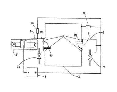
The present invention relates to a plasma generating device comprising a plasma source having a plasma source hollow body (1) and an electron emission unit (5) which makes it possible to emit free electrons into the plasma source hollow body, wherein the plasma source hollow body (1) has a first gas inlet (7a) and a plasma source opening (10) which forms an opening to a vacuum chamber, and further comprising an anode having an anode hollow body (2), wherein the anode hollow body (2) has a second gas inlet (7b) and an anode opening (11) which forms an opening to the vacuum chamber, and a voltage source (8) the negative pole of which is connected to the electron emission unit (5) and the positive pole of which is connected to the anode hollow body (2), wherein the positive pole of the voltage source (8) is additionally electrically connected by means of a first shunt (6a) to the plasma source hollow body.


French Abstract

L'invention concerne un dispositif de génération de plasma, comprenant : - une source de plasma, comprenant un corps creux source de plasma (1) et une unité d'émission d'électrons (5), laquelle permet d'émettre des électrons libres dans le corps creux source de plasma, le corps creux source de plasma (1) comportant une première entrée de gaz (7a) et une ouverture de la source de plasma (10), laquelle forme une ouverture menant à une chambre à vide ; - une anode avec un corps creux anode (2), le corps creux anode (2) comportant une deuxième entrée de gaz (7b) et une ouverture d'anode (11), laquelle forme une ouverture menant à la chambre à vide ; - et une source de tension (8) dont le pôle négatif est relié à l'unité d'émission d'électrons (5) et dont le pôle positif est relié au corps creux anode (2), le pôle positif de la source de tension (8) étant relié en plus électriquement par l'intermédiaire d'une première résistance annexe (6a) au corps creux source de plasma.

Claims

Note: Claims are shown in the official language in which they were submitted.


10
Claims
1. A plasma generating device, comprising:
¨ a plasma source having a plasma source hollow body (1)
and an electron emission unit (5) which allows to emit
free electrons into the plasma source hollow body,
wherein the plasma source hollow body (1) comprises a
first gas inlet (7a) and a plasma source opening (10)
which forms an opening to a vacuum chamber,
¨ an anode comprising an anode hollow body (2), wherein
the anode hollow body (2) comprises a second gas inlet
(7b) and an anode opening (11) which forms an opening
to the vacuum chamber, and
¨ a voltage source (8) the negative pole of which is
connected to the electron emission unit (5) and the
positive pole of which is connected to the anode
hollow body (2),
characterized in that the positive pole of the voltage
source (8) is additionally electrically connected to the
plasma source hollow body by means of a first shunt
(6a).
2. The plasma generating device according to claim 1,
characterized in that the positive pole of the voltage
source (8) is electrically connected to the vacuum chamber
by means of a second shunt (6b).

11
3. The plasma generating device according to claim 1 or
2, characterized in that the plasma source opening (10) is
provided with a screen (9b) which is adapted to close the
plasma source opening as needed.
4. The plasma generating device according to any one of
claims 1 to 3, characterized in that the anode opening (11)
is provided with a screen (9a) which is adapted to close
the anode opening (11) as needed.
5. The plasma generating device according to any one of
claims 1 to 4, characterized in that the plasma source
opening and/or the anode opening are formed such that
supersonic flow through the opening and/or the openings is
established during operation.
6. A method for coating of substrates by means of PE-CVD,
comprising intake of a mono gas and/or polymer gas into a
vacuum chamber comprising a plasma generating device, and
establishing a plasma into the vacuum chamber by means of
the plasma generating device, and applying negative voltage
to the substrates to be coated, characterized in that the
plasma generating device is a plasma generating device
according to claim 5 and therefore neither the inner space
of the plasma hollow body nor the inner space of the anode
hollow body is coated.

Description

Note: Descriptions are shown in the official language in which they were submitted.


CA 02894942 2015-06-12
1
Plasma Source
The present invention relates to a plasma generating device
for generating plasma as well as to a method for generating
plasma in a vacuum coating facility, for example for the
purpose of plasma etching, heating, nitrating and
separating of layers by means of PE-CVD processes.
The invention is based on a plasma source operating based
on the principle of thermal electron emission and applying
a negative voltage to a heated emitter (schottky effect) or
based on the principle of a hollow cathode plasma source.
According to the invention, in the plasma generating
device, the anode comprises an electrically delimited
cavity mounted to a vacuum recipient in a scrolled manner.
This cavity is closed upon deactivation of said plasma by
means of a shutter mechanism, avoiding contamination due to
subsequent process steps. Preferably, activation of the
plasma source is ensured by means of shunts.
The invention is exemplified in detail having regard to the
figures.
In the drawings is shown:

2
Fig. 1: shows a plasma generating device comprising
a plasma source, a hollow anode and ignition
aids;
Fig. 2: shows a representation of an etching
distribution: etching rate in relation to
the substrate position;
Fig. 3a-3f: show modifications of the arrangement of the
plasma source and hollow anode;
Fig. 4: shows an arrangement of the plasma source
and hollow anode in facilities having larger
loading height;
Fig. 5: shows a plurality of anode hollow bodies and
a switching unit; and
Fig. 6a-6b: show a plasma hollow body and an anode
hollow body having a magnetic field
generation apparatus.
Figure 1 shows an inventive plasma generating device for
the treatment of workpieces, for example prior or during
coating in a vacuum facility. Shown is a vacuum chamber 3
comprising a plasma source hollow body 1 being part of a
plasma source, wherein the plasma source hollow body 1 is
flange mounted in an electrically insulated manner via
insulators. The plasma source further comprises an electron
emission unit 5 which is used to produce free electrons.
These means protrude into the plasma source hollow body 1,
such that the electrons are generated into the plasma
source hollow body 1. For example, a tungsten filament
heated to a temperature of about 2700-3000K can be used as
electron emission unit 5. Application of a negative voltage
to the electron emission unit 5 by means of a voltage
CA 2894942 2020-01-30

CA 02894942 2015-06-12
3
source 8 results to the creation of an electron emitter.
Gas is introduced into the plasma source hollow body 1 via
a gas inlet 7a. The gas is ionized by means of free
electrons produced by means of the electron emission unit
5. The gas can comprise argon, for example.
The positive pole of the voltage source 8 is electrically
connected to the plasma source hollow body 1 by means of a
plasma source shunt (PSsR). A current can flow through said
shunt 6a upon activation of the voltage source, realizing
feeding of energy into the plasma in the plasma source
hollow body 1. The resulting plasma in the plasma source
hollow body 1 extends through a plasma source opening 10
provided in the plasma source hollow body 1 into the space
of the vacuum chamber 3 and fills said space.
Further, an additional hollow body is flange-mounted,
electrically insulated, to the vacuum chamber 3 via
insulators 4, wherein the additional hollow body is
referred to as anode hollow body 2 in the following. The
vacuum chamber 3 and the anode hollow body 2 are connected
to each other via an anode opening 11. The anode hollow
body 2 is directly electrically connected to the positive
pole of the voltage source 8. The anode hollow body 2 is
provided with a gas inlet 7b through which gas is
introduced into the anode hollow body 2. This gas can be
argon, for example.

CA 02894942 2015-06-12
4
Further, the wall of the vacuum chamber 3 is connected to
the voltage source 8 via a second shunt 6b. Therefore, flow
of a discharge current from the electron emission unit 5 to
the chamber wall is accomplished. Since the anode hollow
body 2 is directly connected to the positive pole of the
voltage source 8, a discharge occurs through the anode
hollow body 2 and plasma is built-up into the anode hollow
body. Hence, a path which is high-current qualified is
closed, which can receive a very high discharge current at
lower voltages. The current can be some 100 amperes at a
voltage of about 16V to 100V.
The characteristics of the plasma which is generated in
this way, largely depend on the plasma source opening 10
and the anode opening 11. The electrons are accelerated
along said openings due to a potential drop, and further a
very strong ionization thereof occurs in front of as well
as inside the openings due to the presence of argon gas
atoms, for example. Advantageously, the diameter of said
openings is in the range of 4mm and 30mm. Advantageously,
the diameters are about 12mm. The distance between the
plasma source and the hollow anode is in the range of 200
to 400mm. The distance between the openings of the
substrates to be treated is in the range of 200 to 400mm.
In the following, additional typical operation parameters
are exemplified:

CA 02894942 2015-06-12
Gas inlet argon: 50-200sccm into the
plasma source and/or
hollow anode
Discharge current: 200A
Discharge voltage plasma source: 16V - 30V
Discharge voltage hollow anode: 16 - 100V
The power converted into the plasma source and hollow anode
needs to be conveyed away by means of measures known to the
person skilled in the art (not shown in figure 1).
The plasma generating device as mentioned above realizes
performance of a stable plasma method.
Maintenance prior to each process start, which maintenance
is necessary as known so far, can be eliminated by means of
the inventive plasma generating device, in particular by
means of protecting the anode prior to the coating by means
of screens. During the etching process the screen in front
of the anode opening is opened, such that plasma can be
established into the hollow anode. The screen can be closed
by means of a shutter in order to allow an optional
subsequent coating process, for example arc evaporation or
sputtering (sputter). The same relates to the opening 10 of
the plasma source to the vacuum chamber.

CA 02894942 2015-06-12
6
Compared to the prior art, since the anode itself is
actively operated as a plasma source, the plasma volume is
raised. Advantageously, the plasma generating device can be
employed for plasma etching, plasma heating and for PECVD
coating, for example.
For example, argon and hydrogen can be employed for plasma
heating, resulting in the generation of atomic hydrogen
having high reactivity and which is suitable for the
removal of organic residuals.
In the course of PE-CVD coating, argon can be used as purge
gas for the plasma source as well as the hollow anode, for
example. In the course of coating, if for example C2H2
and/or CH4 or gas of a further monomer or polymer is
introduced into the vacuum chamber, a carbon containing
layer, for example a DLC layer (diamond like carbon), is
deposited in the plasma and by using a negative substrate
voltage. In case of the openings 10,11 of the plasma source
and the hollow anode are formed correspondingly, a
supersonic flow occurs therein. This, in addition to the
high energy density, prevents coating of the plasma source
and/or hollow anode. Hence, corresponding inner surfaces
substantially remain uncoated and hence electrically
conductive, which substantially contributes to process
stability.

7
Figure 3 shows modifications of the arrangement of the
plasma source and hollow anode, showing the inventive
plasma generating device. In doing so, arrow tips always
point to a hollow anode and the ends of arrows reside in
the vicinity of a plasma source. The wiring corresponds to
that of Figure 1. Figure 3a shows a simple flange-mounting
to the sidewall of a vacuum chamber. Figures 3b, 3c, 3d,
and 3f show a flange-mounting of two plasma sources and two
anodes, wherein the flow directions exhibit different
spatial orientations. Figure 3e schematically illustrates
flange-mounting of a plasma source to the ceiling of the
vacuum chamber, and the flange mounting of a hollow anode
to the bottom of the vacuum chamber. Vacuum chambers having
a higher loading height allow the arrangement of two
inventive plasma generation devices one over the other.
This is mutatis mutandis schematically shown in Figure 4.
Advantageously, the shunts 6a and 6b mentioned in this
specification are in the range of 10 Ohm to 100 Ohm,
further advantageously in the range of 20 Ohm to 50 Ohm.
Advantageously, the plasma produced on the anode body is
used solely. Therefore, in a further preferred embodiment,
a plurality of anode hollow bodies by at least one plasma
source hollow body are electrically driven by means of
simultaneously or sequentially or overlapping activation of
the switches of the switching unit 12. This is depicted in
Figure 5, wherein means for igniting the discharge are
omitted for the sake of simplicity.
CA 2894942 2020-01-30

CA 02894942 2015-06-12
8
According to a further embodiment of the present invention
the discharge voltage at the anode can be increased by
usage of magnetic fields. This resides to an acceleration
of ions produced at the entrance opening of the anode
hollow body as well as associated high-energy particles.
Further, magnetic fields can be employed at the plasma
source hollow body.
Figures 6a and 6b show a plasma hollow body and an anode
hollow body having a magnetic field generation apparatus
13a and 13b.
While the magnetic field of the plasma hollow body 13b
accomplishes guidance of the electrons and hence the ions
into the vacuum recipient, the magnetic field 13a at the
anode hollow body causes deflection of the electrons and
hence increased voltage drop in front of the anode (hall
effect). However, this potential accelerates ionized gas
atoms and imparts increased energy thereof.
List of reference signs
1 Plasma source hollow body
2 Anode hollow body
3 Vacuum recipient
4 Insulators
Electron emission unit (for example a filament and
feeding)

CA 02894942 2015-06-12
9
6a Shunt plasma source
6b Shunt anode
7a Gas inlet plasma source
7b Gas inlet anode
8 Voltage source
9a Screen in front of anode opening
9b Screen in front of plasma source opening
Opening of the plasma source
11 Opening of the anode
12 Switching unit
13a Magnetic field means
13b Magnetic field means

Representative Drawing
A single figure which represents the drawing illustrating the invention.
Administrative Status

For a clearer understanding of the status of the application/patent presented on this page, the site Disclaimer , as well as the definitions for Patent , Administrative Status , Maintenance Fee  and Payment History  should be consulted.

Administrative Status

Title Date
Forecasted Issue Date 2021-01-05
(86) PCT Filing Date 2013-12-09
(87) PCT Publication Date 2014-06-19
(85) National Entry 2015-06-12
Examination Requested 2018-12-06
(45) Issued 2021-01-05

Abandonment History

There is no abandonment history.

Maintenance Fee

Last Payment of $263.14 was received on 2023-10-27


 Upcoming maintenance fee amounts

Description Date Amount
Next Payment if standard fee 2024-12-09 $347.00
Next Payment if small entity fee 2024-12-09 $125.00

Note : If the full payment has not been received on or before the date indicated, a further fee may be required which may be one of the following

  • the reinstatement fee;
  • the late payment fee; or
  • additional fee to reverse deemed expiry.

Patent fees are adjusted on the 1st of January every year. The amounts above are the current amounts if received by December 31 of the current year.
Please refer to the CIPO Patent Fees web page to see all current fee amounts.

Payment History

Fee Type Anniversary Year Due Date Amount Paid Paid Date
Application Fee $400.00 2015-06-12
Maintenance Fee - Application - New Act 2 2015-12-09 $100.00 2015-12-09
Maintenance Fee - Application - New Act 3 2016-12-09 $100.00 2016-11-09
Maintenance Fee - Application - New Act 4 2017-12-11 $100.00 2017-11-07
Maintenance Fee - Application - New Act 5 2018-12-10 $200.00 2018-11-27
Request for Examination $800.00 2018-12-06
Registration of a document - section 124 $100.00 2019-04-03
Maintenance Fee - Application - New Act 6 2019-12-09 $200.00 2019-11-27
Final Fee 2020-12-04 $300.00 2020-10-27
Maintenance Fee - Application - New Act 7 2020-12-09 $200.00 2020-11-23
Maintenance Fee - Patent - New Act 8 2021-12-09 $204.00 2021-12-09
Maintenance Fee - Patent - New Act 9 2022-12-09 $203.59 2022-12-01
Maintenance Fee - Patent - New Act 10 2023-12-11 $263.14 2023-10-27
Owners on Record

Note: Records showing the ownership history in alphabetical order.

Current Owners on Record
OERLIKON SURFACE SOLUTIONS AG, PFAFFIKON
Past Owners on Record
OERLIKON SURFACE SOLUTIONS AG, TRUBBACH
Past Owners that do not appear in the "Owners on Record" listing will appear in other documentation within the application.
Documents

To view selected files, please enter reCAPTCHA code :


To view images, click a link in the Document Description column. To download the documents, select one or more checkboxes in the first column and then click the "Download Selected in PDF format (Zip Archive)" or the "Download Selected as Single PDF" button.

List of published and non-published patent-specific documents on the CPD .

If you have any difficulty accessing content, you can call the Client Service Centre at 1-866-997-1936 or send them an e-mail at CIPO Client Service Centre.


Document
Description 
Date
(yyyy-mm-dd) 
Number of pages   Size of Image (KB) 
Amendment 2020-01-30 17 507
Description 2020-01-30 9 261
Claims 2020-01-30 2 58
Drawings 2020-01-30 5 104
Final Fee 2020-10-27 4 123
Representative Drawing 2020-12-09 1 10
Cover Page 2020-12-09 1 44
Description 2015-06-12 9 249
Drawings 2015-06-12 5 109
Claims 2015-06-12 2 56
Abstract 2015-06-12 1 23
Representative Drawing 2015-06-12 1 24
Cover Page 2015-08-03 2 56
Request for Examination 2018-12-06 2 55
Patent Cooperation Treaty (PCT) 2015-06-12 4 168
Patent Cooperation Treaty (PCT) 2015-06-12 1 38
International Preliminary Report Received 2015-06-12 14 481
International Search Report 2015-06-12 6 153
National Entry Request 2015-06-12 3 84
Examiner Requisition 2019-09-18 4 235