Note: Descriptions are shown in the official language in which they were submitted.
IMPLANTABLE MEDICAL DEVICE
FOR MINIMALLY-INVASIVE INSERTION
Cross-Reference to Related Applications
The present application claims priority to and the benefit of U.S. Provisional
Patent
Application No. 61/745,086, filed December 21, 2012.
Field of the Disclosure
The present disclosure relates generally to multi-reservoir containment
devices,
including but not limited to medical devices, such as implantable medical
devices, having
.. containment reservoirs for confining substance or subcomponents for
precisely controlled
exposure or release. In certain aspects, the present disclosure relates to
improved designs of
such devices configured for insertion into a patient via minimally invasive
instruments, such
as trocars, catheters, injectors, and the like.
Background
Typical implantable medical devices, such as pacemakers and implantable
cardioverter defibrillators, are designed with two or more housing components
or shells that
contain the control electronics, power source, and other device specific
components. A
header is also used to provide electrical connections into and out of the
device. The housing
and header (or feedthrough) are designed to be hermetic to prevent liquid or
gas exchange
between the internal components (which are typically not biocompatible) and
body fluids. It
is noted, however, that certain implants with epoxy based headers do not
achieve long term
hermeticity. Design and manufacturing methods of implantable devices have
evolved with
the goal of ensuring hermeticity.
MicroCHIPS Inc. designs and manufactures implantable devices based on
microchips
that include reservoir arrays containing biosensors or drugs, for example.
FIG. 1 shows a
possible conventional approach for assembly of components in an implantable
medical device
10, which includes a microchip assembly 12. The microchip assembly 12, which
is also
referred to as a microchip element, includes microreservoirs, each of which
may contain a
drug for controlled delivery in vivo or a sensor for controlled exposure in
vivo. The microchip
assembly 12 is attached to a feedthrough 16 that is welded to the housing 14.
Such microchip
1
CA 2895235 2020-03-03
assemblies or elements are described, for example, in U.S. Patent 7,510,551 to
Uhland et al.
and U.S. Patent 7,604,628 to Santini Jr. et al. The feedthrough 16 contains
electrically
conductive pins that are metallurgically brazed to metallized surfaces on and
through an
alumina disc. A typical pin count exceeds 100, and in more complex designs,
can be over
400. The consequence of such designs is that each pin connection potentially
can be a leak
point.
In addition, each feedthrough pin is electrically connected to an electronic
component
inside the housing. Some designs utilize a wire from the pin to the circuit,
while the
illustrated design attaches the feedthrough 16 directly to a conventional
plastic circuit board
18 (which generally would be unsuitable for continuous in vivo contact with
the patient).
These electrical connections require testing to ensure continuity. As a
result, the pin count
impacts the cost of the feedthrough, and that cost increases as the number of
feedthrough pins
increases in the implantable device. Consequently, due to this complex design
requirement,
the resulting manufacturing, and the required acceptance tests, the
feedthrough is a relatively
expensive component.
Another disadvantage of conventional implantable device designs based on a
feedthrough or header attached to housing components is that the overall
volume of the
resulting device is larger than ideally desired, because several discrete
components make up
the assembly.
Furthermore, electronic-based implantable devices that use radio frequency to
wireles sly transfer information in and out of the body require an antenna.
Radio frequency
waves are significantly attenuated when the antenna is placed in a
conventional metallic
housing, and therefore, the antenna typically is placed on the surface of the
housing, utilizing
the existing feedthrough or another feedthrough dedicated for this
application.
It therefore would be desirable to eliminate or mitigate any or all of the
foregoing
disadvantages associated with conventional designs of implantable medical
devices. In one
particular need, it would be desirable to provide improved housing hermeticity
(e.g., fewer
potential leak paths), simpler construction, and a smaller overall device
volume.
In conjunction with the desire to provide improved hermetic reservoir devices,
it
would also be advantageous to improve the manner in which such actively-
controlled
2
CA 2895235 2020-03-03
reservoir devices can be operably deployed into a patient in need thereof. For
example, it
would be desirable to reduce the size of incisions and/or increase the
possible range of tissue
sites into which the device can be suitably deployed without undue pain or
discomfort to the
patient. It would be desirable to provide device configurations conducive to
such uses in
patients.
Summary
Some or all of the above needs and/or problems may be addressed by one or more
embodiments described herein. In one embodiment, a containment device is
provided that
includes an elongated microchip element having one or more containment
reservoirs that are
configured to be electrically activated to open. The containment device also
includes an
elongated electronic printed circuit board (PCB) comprising a biocompatible
substrate. The
elongated PCB also comprises a first side on which one or more electronic
components are
fixed and an opposed second side on which the elongated microchip element is
fixed in
electrical connection to the one or more electronic components. Further, the
containment
device includes an elongated housing fixed to the elongated PCB. The elongated
housing is
configured to hermetically seal the one or more electronic components of the
elongated PCB
within the elongated housing.
In one aspect there is provided a containment device, comprising an elongated
microchip element comprising one or more containment reservoirs that are
configured to be
electrically activated to open; an elongated electronic printed circuit board
(PCB), wherein the
elongated PCB comprises a first side on which one or more electronic
components are fixed
and an opposed second side on which the elongated microchip element is fixed
in electrical
connection to the one or more electronic components; and an elongated housing
fixed to the
elongated PCB, wherein the elongated housing is configured to surround the
first side of the
elongated PCB such that the elongated housing and the elongated PCB
collectively form a
hermetic enclosure around the one or more electronic components to
hermetically seal the one
or more electronic components of the elongated PCB within the elongated
housing.
In another aspect there is provided a containment device, comprising a
microchip
element comprising one or more containment reservoirs that are configured to
be electrically
3
CA 2895235 2020-03-03
activated to open; an electronic printed circuit board (PCB) comprising a
biocompatible
substrate, wherein the PCB comprises a first side on which one or more
electronic
components are fixed and an opposed second side on which the microchip element
is fixed in
electrical connection to the one or more electronic components; and a housing
fixed to the
PCB, wherein the housing is configured to surround the first side of the PCB
such that the
housing and the PCB collectively form a hermetic enclosure around the one or
more
electronic components to hermetically seal the one or more electronic
components of the PCB
within the housing, wherein the containment device comprises an elongated
tubular structure
configured to be injected in a human or animal subject via a medical
instrument.
In a third aspect there is provided a method of assembling a containment
device,
comprising providing an elongated microchip element comprising one or more
containment
reservoirs that are configured to be electrically activated to open; fixing
the elongated
microchip element to a first side of an elongated electronic printed circuit
board (PCB) which
comprises a biocompatible substrate; electrically connecting the elongated
microchip element
to one or more electronic components which are fixed on a second side of the
elongated PCB;
and hermetically sealing the one or more electronic components of the
elongated PCB within
an elongated housing that is fixed to the elongated PCB by surrounding the
first side of the
elongated PCB such that the elongated housing and the elongated PCB
collectively form a
hermetic enclosure around the one or more electronic components.
In a further aspect there is provided A containment device, comprising an
elongated
microchip element comprising one or more containment reservoirs that are
configured to be
electrically activated to open; an elongated electronic printed circuit board
(PCB) which
comprises a biocompatible and hermetic substrate material, wherein the
elongated PCB
comprises a first side on which one or more electronic components are fixed
and an opposed
second side on which the elongated microchip element is fixed in electrical
connection to the
one or more electronic components without using a feedthrough to operably
connect the
microchip element to the PCB; and an elongated housing fixed to the elongated
PCB, wherein
the elongated housing and the elongated PCB together form a hermetic enclosure
around the
one or more electronic components.
3a
23403563.1
CA 2895235 2020-03-03
In yet another aspect there is provided, A containment device, comprising a
microchip
element comprising one or more containment reservoirs that are configured to
be electrically
activated to open; an electronic printed circuit board (PCB) comprising a
biocompatible and
hermetic substrate, wherein the PCB comprises a first side on which one or
more electronic
components are fixed and an opposed second side on which the microchip element
is directly
fixed, without an interposed feedthrough, in electrical connection to the one
or more
electronic components; and a housing fixed to the PCB, wherein the housing and
the PCB
together are configured to hermetically seal the one or more electronic
components of the
PCB within the housing, wherein the containment device comprises an elongated
tubular
structure configured to be injected in a human or animal subject.
Other embodiments, aspects, and features of the containment device will become
apparent to those skilled in the art from the following detailed description,
the accompanying
drawings, and the appended claims.
Brief Description of the Drawings
Reference will now be made to the accompanying drawings, which are not
necessarily
drawn to scale.
FIG. 1 schematically depicts an exploded perspective view of a prior art
containment
device including a microchip assembly.
FIG. 2A schematically depicts a cross-sectional view of an assembled
containment
device including a microchip assembly according to an embodiment.
3b
23403563.1
CA 2895235 2020-03-03
CA 02895235 2015-06-15
WO 2014/100555 PCT/US2013/076849
FIG. 2B schematically depicts an exploded cross-sectional view of the
containment
device shown in FIG. 2A.
FIG. 2C schematically depicts a top view of the containment device shown in
FIGS.
2A and 2B.
FIG. 3 schematically depicts a perspective view of the containment device
illustrated
in FIGS. 2A-2C.
FIG. 4 schematically depicts a close-up, cross-sectional view of a portion of
a
containment device according to an embodiment.
FIG. 5A schematically depicts a cross-sectional view of a microchip element
assembly according to an embodiment.
FIG. 5B schematically depicts an exploded cross-sectional view of the
microchip
element assembly shown in FIG. 5A.
FIG. 6 schematically depicts a cross-sectional close-up view of a portion of
an
assembled containment device including a microchip assembly according to an
embodiment.
DETAILED DESCRIPTION
Illustrative embodiments will now be described more fully hereinafter with
reference
to the accompanying drawings, in which some, but not all embodiments are
shown. The
representative embodiments described in the disclosure may be embodied in many
different
forms and should not be construed as limited to the embodiments set forth
herein. Like
.. numbers refer to like elements throughout.
The containment devices and assemblies described herein provide, among other
advantages, significantly improved space efficiency of the assembled devices.
For example,
compared with prior art devices, embodiments of the present devices can hold
the same or a
larger drug payload is the same or a smaller overall device volume. Moreover,
in certain
.. embodiments, the devices and methods advantageously eliminate the need for
a costly and
complex feedthrough, provide a thinner, sleek implant due to the elimination
of the
feedthrough, provide improved reliability by eliminating numerous feedthrough
pins and
electrical connections, provide improved reliability by reducing the number of
hermetic
interfaces, simplify tests to confirm functionality, and provide a simpler
assembly. This can
be particularly important in embodiments in which the containment device is an
implantable
4
CA 02895235 2015-06-15
WO 2014/100555 PCT/US2013/076849
medical device intended for long-term implantation in a human or animal
subject via
minimally-invasive insertion means, such as through a small incision, trocar,
cannula,
injector, or similar like medical instrument.
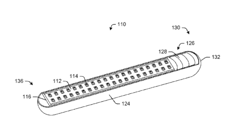
The containment devices provided herein may be further understood with
reference to
the following exemplary embodiments, including the containment device 110
illustrated in
FIGS. 2A-3. The containment device 110 includes an elongated microchip element
112
which comprises one or more containment reservoirs 114 that can be
electrically activated to
open. The containment device 110 also includes an elongated electronic printed
circuit board
(PCB) 116. The elongated PCB 116 comprises a biocompatible substrate and has a
first side
118 on which one or more electronic components 120 are fixed and an opposed
second side
122 on which the microchip element 112 is fixed in electrical connection to
the one or more
electronic components 120. As will be explained below with reference to FIG.
4, the
electronic components 120 on the first side 118 of the PCB 116 are in
electrical (i.e.,
operable) communication with the microchip element 112.
It is understood that the containment device 110 may include any suitable
number of
microchip elements 112 (e.g., from 1 to 6) and that each microchip element 112
may include a
plurality of discrete containment reservoirs 114 (e.g., from 10 to 750
reservoirs). More
microchip elements 112, and fewer or more containment reservoirs 114, per
containment
device 110 are also envisioned. Moreover, it is understood that the
containment device 110
may include any suitable number of PCBs 116.
As shown in FIGS. 2A-2C, embodiments particularly suitable for minimally
invasive
insertion into a patient may have long, narrow microchip elements 112 with
elongated arrays
of closely spaced containment reservoirs. FIG. 2C shows a 2 x 28 reservoirs
array. In one
embodiment, the elongated array has from 1 to 4 rows of 20 to 40 reservoirs.
In other
embodiments, other numbers of rows and reservoirs are envisioned.
The "electronic printed circuit board" (PCB) refers to a substrate that
mechanically
supports and electrically connects electronic components using conductive
pathways, tracks,
or signal traces as known in the art. In embodiments, the PCB includes a
biocompatible and
hermetic substrate material. Suitable such materials include ceramics, such as
alumina and
silicon nitride. Multi-layer alumina PCBs have been successfully designed and
manufactured.
5
CA 02895235 2015-06-15
WO 2014/100555 PCT/US2013/076849
See, for example, U.S. Patent Application Publication No. 2003/0034564. These
laminations
may be the result of combining conductive layers, dielectric layers, and
aluminum oxide
(A1203, alumina) in a low temperature co-fired process. The alumina is
referred to as low
temperature co-fired ceramic (LTCC). These biocompatible ceramics also
function as a
hermetic barrier, eliminating the need, in some instances, for conventional
metallic housing
elements. Other materials or combinations of materials capable of performing
all or some of
the described function may also be used.
The term "biocompatible" as used herein generally refers to materials of
construction
that are suitable for long-term or short-term implantation into a human or
animal subject, e.g.,
a patient. Such materials of constructions are known in the art of implantable
medical
devices.
As used herein, the term "hermetic seal" refers to preventing undesirable
ingress or
egress of chemicals (e.g., water vapor, water, oxygen, etc.) into or from one
or more
compartments of the device, such as the device reservoirs or housings, over
the useful life of
the device. For purposes herein, a material/seal that transmits helium (He) at
a rate less than
1x10⁻⁹ atm*cc/sec is termed hermetic.
The containment device 110 may include an elongated housing 124. The elongated
housing 124 is configured to hermetically seal the one or more electronic
components 120 of
the elongated PCB 116 within the elongated housing 124. That is, the elongated
housing 124
is configured to surround the first side 118 of the elongated PCB 116. In this
manner, the
elongated housing 124 and the elongated PCB 116 collectively form a hermetic
enclosure
around the one or more electronic components 120. Desirably, the elongated
housing 124 and
at least a portion of the outward facing second side 122 of the elongated PCB
114 are formed
of a biocompatible material. For example, in some instances, the elongated
housing 124 may
be made of a biocompatible metal or alloy, such as titanium or stainless
steel. In other
instances, the elongated housing 124 may be made of a biocompatible polymer.
In certain
embodiments, at least a portion of the elongated housing 124 has a generally
cylindrical body.
In some instances, the elongated housing 124 includes atraumatic surfaces.
Moreover, a distal
end 136 of the elongated housing 124 may be rounded.
6
CA 02895235 2015-06-15
WO 2014/100555 PCT/US2013/076849
The elongated housing 124 may comprise a battery chamber 126 configured to
house
one or more batteries 128 therein. Any power source or power system may be
housed within
the battery chamber 126. In some instances, the battery chamber 126 may be a
separate area
within the elongated housing 124. In other instances, the battery chamber 126
may be part of
a single enclosure formed by the elongated housing 124. In one embodiment, the
battery
chamber 126 may be positioned about a proximal end 130 of the elongated
housing 124.
However, the battery chamber 126 may be located at any position within the
elongated
housing 124. Moreover, in some instances, the battery chamber 126 may be
omitted. For
example, the device power may be provided by inductive charging.
In certain embodiments, the battery chamber 126 may include a cover 132. The
cover
132 may be removable or permanent. The cover 132 may be configured to provide
access to
the batteries 128 and/or hermetically seal the one or more batteries 128
within the battery
chamber 126. That is, in a preferred embodiment, the cover 132 and the
elongated housing
124 form a hermetic seal when affixed to each other. In one example, the cover
132 may be
located about the proximal end 130 of the elongated housing 124.
The interface of the elongated housing 124 with the elongated PCB 116, in a
preferred
embodiment, forms a hermetic seal to isolate the one or more electronic
components 120
within the elongated housing 124. In some instances, the elongated housing 124
may be
welded to the elongated PCB 116. In other instances, a biocompatible substance
134, such as
a biocompatible epoxy coating (e.g., an epoxy resin) or other biocompatible
coating material,
may be disposed over at least a portion of the elongated microchip element
112, the elongated
PCB 116, and the elongated housing 124. This coating may be multilayered, and
it may
include a hermetic material so long the material does not interfere with the
operation of any of
the components, such as the electronic components 120 or the batteries 128.
In certain embodiments, the containment device 110 may include a sleek,
tubular
profile. For example, some or all of the components associated with the
containment device
110 may be elongated. That is, some or all of the components of the
containment device 110,
such as the elongated microchip element 112, the elongated PCB 116, and the
elongated
housing 124, may have a greater length than width. Furthermore, the
biocompatible coating
substance 134, the elongated microchip element 112, and the elongated housing
124 may
7
CA 02895235 2015-06-15
WO 2014/100555 PCT/US2013/076849
collectively form a generally circular cross-section and rounded distal end
136 of the
containment device 110. The components may collectively fit together to form a
sleek, tube-
like structure or assembly that may be inserted in a human or animal subject
in a minimally
invasive manner. The sleek, tube-like structure or assembly preferably has
atraumatic
surfaces.
The biocompatible coating substance 134 may create an atraumatic surface about
the
containment device 110. In certain embodiments, the surface of the containment
device is
formed of or coated with a lubricious substance to facilitate passage of the
device to the
intended tissue site.
The containment device 110 may be implanted in a human or animal subject, such
as a
patient in need of treatment, diagnosis, or prophylaxis, by a variety of
techniques known in
the art. In a preferred embodiment, the device is inserted into the patient at
a subcutaneous
tissue site. A variety of insertion tools and systems may be used depending on
the particular
size of the implant and the particular site of implantation desired for a
particular medical
.. purpose. The containment device 110 may be inserted, injected, or otherwise
placed into the
human or animal subject via one or a combination of minimally invasive medical
instruments,
including a cannula, trocar, subcutaneous insert, or a gun-like injector
device or assembly. In
one embodiment, a small (e.g., few millimeters) incision is made in the
patient's skin, and the
containment device 110 is passed through the incision and into the patient
just under the skin
using a long, narrow inserter tool that can grasp an end of the containment
device 110 in a
linear low profile arrangement. The containment device 110 would be released
from the
inserter tool, the end of the inserter tool would be removed from the
incision, and then the
incision would be closed, for example with one or a few stitches. In some
instances, one or
more suture loops may be provided with the housing 124 and/or the cap 132. The
suture
loops may be configured to anchor the containment device 110 in a subcutaneous
space.
The electronic components 120 provide any of a number of functions for the
containment device 110. Examples include, but are not limited to, a controller
(e.g., one or
more microprocessors) and power source (e.g., a battery or capacitor) for
electrically
activating the reservoir 114 to cause it to become opened and/to communicate
with a sensor,
for example, located within the reservoir 114 or with another device remotely
located from
8
the containment device 110. Other electronic components may include, for
example,
telemetry hardware, capacitors, transistors, and diodes, as well as the
control means for
actuating the reservoir caps. The control means may include an input source, a
microprocessor, a timer, a demultiplexer (or multiplexer). In an embodiment,
the electronic
components include components for wirelessly receiving energy for charging an
on-board
storage capacitor, which may further reduce the space requirements for the
electronic
components on-board the containment device 110. In some instances, the
electronic
components may include an antenna, such as a transmitter, receiver, or
transceiver.
The containment reservoir 114 of the microchip element 112 may be configured
to
open/activate in a variety of ways, which may be known in the art. In one
embodiment, the
containment reservoir 114 is structured and configured to be electrically
activated to open as
described in U.S. Patent No. 7, 510,551 and U.S. Patent No. 7,604,628.
One embodiment of the electrical connection between a PCB/electronic
components
and a microchip element is illustrated in FIG. 4. The figure shows part of the
microchip
element 312 including two containment reservoirs 344. Each containment
reservoir 344 has
an opening that is (initially) closed off by a reservoir cap 348. The
containment reservoir 344,
which is formed at least in part in a substrate 343, has a closed end opposed
to the opening
and a sidewall therebetween. The microchip element 312 is secured to a side of
a PCB 314,
and electronic component 318 is secured on the opposed side of the PCB 314.
The PCB 314
includes a via 330 which electrically connects electronic component 318 to the
microchip
element 312. Via 330 is mechanically and electrically connected to metallized
conductive
surfaces 332A, 332B on the PCB 314, and the microchip element 312 is
wirebonded 334 to
the metallized conductive surface 332A. Any via or wirebond combination may be
used. A
biocompatible coating substance 336 is applied over the wire bond to secure
and protect the
connection, and typically will coat part of the surface of the PCB 314, part
of the microchip
element 312, and part of the housing 320 but not the reservoir caps 348. The
coating
substance 336 may be a polymer, such as an epoxy or other resin. Any suitable
coating may
be used.
9
CA 2895235 2020-03-03
In one embodiment, the reservoir caps 348 are structured and configured to be
electrically activated to open as described in U.S. Patent No. 7, 510,551 and
U.S. Patent No.
7,604,628. That is, in a preferred embodiment, the reservoirs are configured
to open by being
disintegrated by electrothermal ablation. The reservoir caps 348 may be formed
of a metal
film, which may comprise a single layer or a laminate structure. For example,
the reservoir
cap 348 may comprise gold, platinum, titanium, or a combination thereof. In
other
embodiments, the reservoir cap 348 can be configured to be activated or opened
by a
mechanical or electrochemical mechanism.
The containment reservoir of the microchip element may be a "microreservoir"
which
generally refers to a reservoir having a volume equal to or less than 500 pL
(e.g., less than
250 pL, less than 100 pL, less than 50 pIõ less than 25 L, less than 10 pL,
etc.). In another
embodiment, the containment reservoirs may be a "macroreservoir" which
generally refers to
a reservoir having a volume greater than 500 pt (e.g., greater than 600 AL,
greater than 750
4, greater than 900 pt, greater than 1 mL, etc.) and less than 5 mL (e.g.,
less than 4 mL, less
than 3 mL, less than 2 mL, less than 1 mL, etc.). The terms "reservoir" and
"containment
reservoir" are intended to encompass both microreservoirs and macroreservoirs
unless
explicitly indicated to be limited to one or the other.
In another aspect, improved microchip elements and methods for their
manufacture
are provided. In a preferred embodiment, the microchip device element includes
a relatively
thin silicon substrate bonded to a relatively thicker primary substrate formed
of a polymer or a
glass or other ceramic material. Advantageously, by defining the reservoirs in
the primary
substrate rather than the silicon substrate, the reservoirs may be formed
using processes other
than dry reactive ion etching (DRIE). This is important, not just because DRIE
processes are
expensive, but also because under the conventional process, the DRIE processes
occurred
after deposition of the reservoir cap film, unnecessarily exposing the
reservoir cap film to
subsequent processing, which can negatively impact the yield of acceptable
(e.g., hermetic)
reservoir caps.
In addition, by adding the positive sealing features (e.g., gold sealing
rings) to the
silicon substrate, this keeps all of the high tolerance microfeatures to only
the silicon
substrate, which in turn advantageously frees up the primary substrate to be
made by other,
CA 2895235 2020-03-03
CA 02895235 2015-06-15
WO 2014/100555
PCT/US2013/076849
potentially lower tolerance, manufacturing processes. In this way, the
reservoir can be made
much deeper and thereby increase the unit reservoir payload. In one
embodiment, the primary
substrate is made by a casting or molding process using ceramic or polymeric
materials that
allows for formation of reservoirs that are deeper than conventional
reservoirs and have
smoother side walls than would be readily possible using DRIE. This cast or
molded
substrate then may be gold plated in and about sealing grooves formed therein
for bonding
with the positive sealing features on the silicon substrate.
An exemplary embodiment of the elongated microchip element is illustrated in
FIG.
5A and FIG. 5B. The elongated microchip element 412 includes a primary
substrate 440 and
a silicon substrate 442, which are bonded together. The silicon substrate 442
has a first side,
an opposed second side, and apertures 446 extending therethrough. Three
apertures 446 are
shown for each reservoir 444. The first side of the silicon substrate 442
includes reservoir
caps 448 which close off the apertures 446 until the reservoir needs to be
opened. In a
preferred embodiment, the reservoir caps 448 are electrically conductive. For
example, the
reservoir caps 448 may be in the form of a metal film. The silicon substrate
442, apertures
446, and reservoir caps 448 can be made using microfabrication techniques
known in the art.
For example, the photolithography, etching, and deposition techniques
described in U.S.
Patent No. 7,604,628 may be used to form the apertures 446 in a polysilicon
substrate closed
off by metal reservoir caps 448.
The primary substrate 440 includes two reservoirs 444 in this illustration,
although
more or less reservoirs may be included. Each reservoir 444 is defined by a
closed end wall,
an open end, and at least one sidewall extending between the closed end wall
and the open
end. As mentioned above, the primary substrate 440 may be formed of silicon.
In other
embodiments, the substrate may be formed of a metaloid, polymer, glass, or
other ceramic
material. Any suitable material may be used. The substrate and reservoirs may
be made by
any suitable process, including but not limited to molding, casting,
micromachining, and
build-up or lamination techniques known in the art. In one embodiment, the
primary substrate
440 is made of/by low temperature co-fired ceramics (LTCC). It may further
include a
coating layer on all or a portion of the substrate, for example to provide or
improve
hermeticity, biocompatibility, bonding, and/or reservoir content
compatibility, stability, or
11
release. Depending on the purpose of the coating layer, it may be applied
inside the reservoirs
444, outside of the reservoirs 444, or both. Examples of possible coating
materials include
biocompatible metals, such as gold, and polymers, such as parylene.
The primary substrate 440 and the silicon substrate 442 are bonded together
using any
suitable method, to hermetically seal the reservoirs 444. In this way, the
open end of the
reservoir 444 is in fluid communication with the apertures 446 for controlled
release or
exposure of reservoir contents. In a preferred embodiment, the substrates are
hermetically
sealed together using a compression cold welding process, such as described in
U.S. Patent
No. 8,191,756.
As shown in FIGS. 5A and 58, the second side of the silicon substrate 442
includes
ring structures 452 formed thereon, and the first side of the primary
substrate 440 includes
grooves 450. These bonding features are compressed together to form a cold
weld bond
hermetic seal surrounding the individual reservoirs 444. The ring structures
452 may be
formed by a depositing gold or another metal layer on the silicon substrate
442. The grooves
450 may be etched in the silicon and then coated with a metallized layer of
the same material
as the metal ring. Variations of this embodiment are envisioned, for example,
where other
positive and negative bonding features are provided in/on either or both
interfacing surfaces
of the silicon substrate 442 and the primary substrate 440.
The primary substrate 440 is generally relatively thicker than the silicon
substrate 442,
and all or at least a majority (greater than 50%) of the reservoir sidewall
height (or depth) is
defined by the primary substrate 440. In an embodiment, the silicon substrate
442 has
thickness that is between 5% and 50% of the thickness of the primary substrate
440 at the
bonded interfaces of the substrates.
Although not shown in the FIG. 4 or FIG. 5A, the reservoirs 344 and 444,
respectively, include reservoir contents positioned therewithin. The
reservoirs can be
configured to store essentially any substance or device component in need
hermetic
containment and subsequent release or exposure at a selected time. The
reservoir content may
be, for example, a chemical reagent, a drug formulation, or sensor or
component thereof, such
as an electrode. In an embodiment, a single device includes at least one
containment reservoir
containing a biosensor and at least one reservoir containing a drug
formulation. Examples of
12
CA 2895235 2020-03-03
CA 02895235 2015-06-15
WO 2014/100555
PCT/US2013/076849
various reservoir contents are described for example in U.S. Patent No.
7,510,551; U.S. Patent
No. 7,497,855; U.S. Patent No. 7,604,628; U.S. Patent No. 7,488,316; and PCT
WO
2012/027137.
An exemplary embodiment of a containment device 600 including a microchip
element 612 is illustrated in FIG. 6. The containment device 600 includes a
ceramic PCB
614 which has via 630 electrically connecting electronic component 618 to the
microchip
element 612. The electronic component 618 is secured on a first side of the
ceramic PCB
614, and the microchip element 612 is secured on the opposing second side of
the PCB 614.
The via 630 electrically connects to a metallized conductive surface 632 on
the first side of
the PCB 614. The electrical circuitry 635 of the microchip element 612 is
electrically
connected to the metallized surface 632 by a wirebond 634. An epoxy 633 coats
the wirebond
634 and at least a portion of the microchip element 612, the ceramic PCB 614,
and a housing
620. In this manner, the epoxy 633 ensures that the containment device 600 is
void of any
atraumatic surfaces. The epoxy 633 also may passivatc the wirebond 634. The
second side of
the ceramic PCB 614 also includes a metallized conductive surface 637, which
is electrically
connected to the electronic component 618. Although not shown in this
illustration, the
containment device 600 may include multiple microchip elements, as well as
multiple vias,
electronic components, and wirebonds. Moreover, the containment device 600
(with the
exception of the reservoir caps) may be completely or partially coated by the
epoxy 633.
The microchip element 612 includes a primary substrate 640 and a silicon
substrate
642. The primary substrate 640 and silicon substrate 642 are bonded together
by compression
cold welding at/adjacent the interface of a ring structure and groove
structure tongue 650/652.
Reservoirs 644 are defined in the primary substrate 640 with the open end in
fluid
communication with apertures 646 defined through the silicon substrate 612.
Electrically
.. conductive reservoir caps 648 sealingly cover the apertures 646 and
reservoirs 644.
Modifications and variations of the methods and devices described herein will
be
obvious to those skilled in the art from the foregoing detailed description.
Such modifications
and variations are intended to come within the scope of the appended claims.
13