Note: Descriptions are shown in the official language in which they were submitted.
CA 02895288 2015-06-16
WO 2013/098612
PCT/1B2012/002615
ION OPTICAL ELEMENTS
RELATED APPLICATION
[0001] This application claims the benefit and priority from US Provisional
Application Serial
No. 61/582,071, filed on December 30, 2011, the entire contents of which is
incorporated by
reference herein.
FIELD
[0002] The applicant's teachings relate to ion optical elements and related
methods of making
and using such elements, for example in the field of mass spectrometry.
BACKGROUND
[0003] A number of devices used in mass spectrometry and other fields involve
a high number
of ion optical elements that must be manufactured and assembled with a great
deal of precision.
For example, devices such as time-of-flight reflectrons, time-of-flight
accelerators, ion funnels,
ion tunnels, ion mobility columns, ion mirrors, and so forth can comprise
periodic structures
formed by many electrodes which are separated from one another by insulating
spacers.
[0004] FIG. 1 illustrates a prior art ion mirror 10 that includes a plurality
of axially-aligned ring-
shaped electrodes 12 that define an interior volume 14. Insulating spacers 16
are disposed
between adjacent electrodes 12, and electric potentials are applied to the
electrodes 12 by a
controller 18 to generate an electromagnetic field within the interior volume
14, thereby
influencing an ion beam passing therethrough. In the ion mirror 10 of FIG. 1,
each electrode 12
must be individually machined from a solid piece of electrically-conductive
stock material, such
as stainless steel or nickel-plated aluminum. It can be very difficult and
expensive to machine
such materials with the requisite degree of accuracy. The difficulty and
expense are
compounded by the need to assemble a large number of discrete components with
very tight
tolerances.
[0005] In CORNISH et al., "Miniature Time-Of-Flight Mass Spectrometer Using A
Flexible
Circuitboard Reflector," Rapid Communications in Mass Spectrometry 14, 2408-
2411 (2000),
the entire content of which is incorporated herein by reference, an ion
reflector is constructed by
depositing a series of thin-copper traces on a flexible circuit board
substrate. The substrate is
1
CONFIRMATION COPY
CA 02895288 2015-06-16
WO 2013/098612
PCT/1B2012/002615
then rolled into a tube with the copper traces facing inward to form ring-
shaped electrodes. One
disadvantage with such a structure is that at least some of the ions passing
through the ion
reflector collide with the exposed substrate regions between the copper
traces. Over time, this
can lead to a buildup of electrical charge on said regions and to the
production of corresponding
electromagnetic fields, which can have an unintended and undesired =influence
on the ion beam
passing through the reflector.
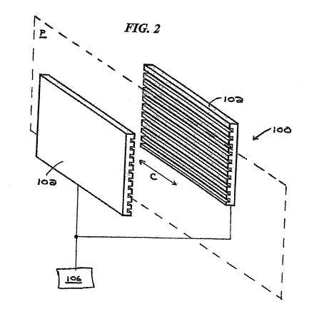
[0006] U.S. Patent No. 6,316,768 to Rockwood et al., entitled "PRINTED CIRCUIT
BOARDS
AS INSULATED COMPONENTS FOR A TIME OF FLIGHT MASS SPECTROMETER," the
entire content of which is incorporated herein by reference, purportedly
addresses this concern
by coating the exposed regions of substrate with a partially conductive
coating that provides a
discharge path to ground. Although this technique is said to prevent charge
buildup between
electrodes, it adds additional complexity, time, and expense to the
manufacturing process, and
reduces the durability and lifespan of the finished device.
[0007] Accordingly, a need exists for improved ion optical elements and
related methods of
making and using the same.
SUMMARY
[0008] In one aspect of at least one embodiment of the applicant's teachings,
an ion optical
element is provided that can comprise a substrate that can comprise first and
second opposed
surfaces and a plurality of protrusions extending from said first surface,
each protrusion having a
top surface, at least one sidewall, and an electrically-conductive coating
disposed on said top
surface and at least a portion of said at least one sidewall. The substrate
can also comprise at
least one recess separating said protrusions, each recess having a portion of
said first surface as a
floor thereof. A depth of each recess can be at least about one half of a
width of said recess.
[0009] Related aspects of at least one embodiment of the applicant's teachings
provide an ion
optical element, e.g., as described above, in which said top surface of at
least some of said
protrusions is planar.
[0010] Related aspects of at least one embodiment of the applicant's teachings
provide an ion
optical element, e.g., as described above, in which said top surface of at
least some of said
protrusions is perpendicular to said at least one sidewall.
2
CA 02895288 2015-06-16
WO 2013/098612
PCT/1B2012/002615
[00111 Related aspects of at least one embodiment of the applicant's teachings
provide an ion
optical element, e.g., as described above, in which said top surface of at
least some of said
protrusions is curved.
[0012] Related aspects of at least one embodiment of the applicant's teachings
provide an ion
optical element, e.g., as described above, in which said at least one sidewall
of at least some of
said protrusions is curved.
[0013] Related aspects of at least one embodiment of the applicant's teachings
provide an ion
optical element, e.g., as described above, in which at least some of said
protrusions comprise an
electrically-conductive via extending through the substrate from the
electrically-conductive
coating of the protrusion to an electrically-conductive pad formed on said
second surface.
[0014] Related aspects of at least one embodiment of the applicant's teachings
provide an ion
optical element, e.g., as described above, in which the via extends from a
portion of the
electrically-conductive coating disposed on the top surface of the protrusion
to said pad.
[0015] Related aspects of at least one embodiment of the applicant's teachings
provide an ion
optical element, e.g., as described above, in which the via extends from a
portion of the
electrically-conductive coating disposed on the at least one sidewall of the
protrusion to said pad.
[0016] Related aspects of at least one embodiment of the applicant's teachings
provide an ion
optical element, e.g., as described above, in which said pad is coupled to at
least one of a resistor,
a resistive film, and a power supply configured to apply an electric potential
thereto.
[0017] Related aspects of at least one embodiment of the applicant's teachings
provide an ion
optical element, e.g., as described above, that can further comprise a vent
extending through the
substrate from the floor of said at least one recess to the second surface
that permits gas flow
therethrough.
[0018] Related aspects of at least one embodiment of the applicant's teachings
provide an ion
optical element, e.g., as described above, in which the substrate comprises
any of an electrically-
insulating material and a semi-conducting material.
[0019] Related aspects of at least one embodiment of the applicant's teachings
provide an ion
optical element, e.g., as described above, in which the substrate comprises a
printed circuit board
material.
3
CA 02895288 2015-06-16
WO 2013/098612
PCT/1B2012/002615
[0020] Related aspects of at least one embodiment of the applicant's teachings
provide an ion
optical element, e.g., as described above, in which the substrate comprises
any of ceramics,
organic polymers, glass, machinable ceramics, and materials used in 3D
printing.
[0021] Related aspects of at least one embodiment of the applicant's teachings
provide an ion
optical element, e.g., as described above, in which the printed circuit board
material is selected
from the group consisting of laminated polyamides, G-10, Teflon-based
materials, phenolic
cotton FR-2, and woven glass FR-4.
[0022] Related aspects of at least one embodiment of the applicant's teachings
provide an ion
optical element, e.g., as described above, in which the electrically-
conductive coating comprises
a non-oxidizing metal.
[0023] Related aspects of at least one embodiment of the applicant's teachings
provide an ion
optical element, e.g., as described above, in which the non-oxidizing metal
comprises at least one
of gold, nickel, platinum, palladium, titanium, stainless steel, tungsten,
copper, and molybdenum.
[0024] Related aspects of at least one embodiment of the applicant's teachings
provide an ion
optical element, e.g., as described above, in which the ion optical element
comprises at least one
of a time-of-flight reflectron, a time-of-flight accelerator, an ion funnel,
an ion tunnel, a multi-
element ion optics lens, and an ion mobility column.
[0025] In another aspect of at least one embodiment of the applicant's
teachings, an ion optical
element, such as an ion guide, for use in a mass spectrometer is provided,
which can comprise an
electrically-insulating substrate having a plurality of protrusions extending
therefrom and a
plurality of recesses separating each of said protrusions, each of said
protrusions having an
electrically-conductive coating disposed thereon to form an electrode. The ion
guide can also
comprise a channel bounded at least in part by said substrate into which said
electrodes protrude
and through which ions can pass, and a controller configured to apply electric
potentials to each
of said electrodes to generate an electromagnetic field within the channel.
Said recesses can
have a depth sufficient to substantially prevent ions passing through the
channel from contacting
a floor surface of said recesses.
[0026] Related aspects of at least one embodiment of the applicant's teachings
provide an ion
optical element, e.g., as described above, in which the substrate is
substantially ring-shaped.
[0027] In another aspect of at least one embodiment of the applicant's
teachings, a method of
manufacturing an ion optical element is provided, which can comprise
selectively removing
4
CA 02895288 2015-06-16
WO 2013/098612
PCT/1B2012/002615
portions of a printed circuit board substrate to generate a plurality of
protrusions, said protrusions
being separated from one another by a plurality of recesses each having a
depth that is at least
about one half of its width, each of said protrusions having a top surface and
at least one
sidewall. The method can also comprise depositing an electrically-conductive
coating on said
top surface and at least a portion of said at least one sidewall of each of
said protrusions, and
forming a non-coated region between each of said protrusions such that the
protrusions define a
plurality of discrete electrodes.
[0028] Related aspects of at least one embodiment of the applicant's teachings
provide a
method, e.g., as described above, in which said electrically-conductive
coating is deposited using
at least one of electroplating and vapor deposition.
[0029] Related aspects of at least one embodiment of the applicant's teachings
provide a
method, e.g., as described above, in which each of said non-coated regions is
formed by applying
a mask to said non-coated region before depositing the electrically-conductive
coating and
removing the mask after depositing the electrically-conductive coating.
[0030] Related aspects of at least one embodiment of the applicant's teachings
provide a
method, e.g., as described above, in which each of said non-coated regions is
formed by
depositing the electrically-conductive coating over floor surfaces of said
recesses, and then
selectively removing said coating from said floor surfaces.
[0031] Related aspects of at least one embodiment of the applicant's teachings
provide a
method, e.g., as described above, in which each of said non-coated regions is
formed by etching
portions of the electrically-conductive coating.
[0032] In another aspect of at least one embodiment of the applicant's
teachings, an ion optical
element is provided, which can comprise a plurality of electrodes positioned
to be spaced apart
from one another, each of said electrodes comprising a core comprising a
printed circuit board
material, the core having an aperture for passage of ions therethrough, and an
electrically-
conductive coating disposed over an entire exterior surface of said core.
[0033] Related aspects of at least one embodiment of the applicant's teachings
provide an ion
optical element, e.g., as described above, in which the electrically-
conductive coating has a
thickness of at least about 2 microns.
5
CA 02895288 2015-06-16
WO 2013/098612
PCT/1B2012/002615
[0034] Related aspects of at least one embodiment of the applicant's teachings
provide an ion
optical element, e.g., as described above, in which the electrically-
conductive coating comprises
a plurality of layers.
[0035] Related aspects of at least one embodiment of the applicant's teachings
provide an ion
optical element, e.g., as described above, in which the electrically-
conductive coating comprises
a first layer deposited directly onto the core and a second layer deposited
onto the first layer.
[0036] Related aspects of at least one embodiment of the applicant's teachings
provide an ion
optical element, e.g., as described above, in which the first layer comprises
a copper coating and
the second layer comprises a gold coating.
[0037] In another aspect of at least one embodiment of the applicant's
teachings, an ion optical
element configured for positioning in a vacuum chamber of a mass spectrometer
is provided.
The ion optical element can comprise a plurality of electrodes positioned to
be spaced apart from
one another. Each of said electrodes can comprise a core comprising a printed
circuit board
material, the core having an aperture for passage of ions therethrough, and an
electrically-
conductive coating disposed over a selected surface area of said core such
that said coating
substantially prevents outgassing from said printed circuit board material
under vacuum
conditions.
[0038] Related aspects of at least one embodiment of the applicant's teachings
provide an ion
optical element, e.g., as described above, in which the electrically-
conductive coating is disposed
over at least about 50 percent, at least about 60 percent, at least about 70
percent, at least about
80 percent, at least about 90 percent, and/or at least about 100 percent of an
exposed surface area
of said core.
[0039] Related aspects of at least one embodiment of the applicant's teachings
provide an ion
optical element, e.g., as described above, in which the electrically-
conductive coating is disposed
over at the entire exposed surface area of said core.
[0040] Related aspects of at least one embodiment of the applicant's teachings
provide an ion
optical element, e.g., as described above, in which the electrically-
conductive coating has a
thickness of at least about 2 microns.
[0041] Related aspects of at least one embodiment of the applicant's teachings
provide an ion
optical element, e.g., as described above, in which the electrically-
conductive coating comprises
a plurality of layers.
6
CA 02895288 2015-06-16
WO 2013/098612
PCT/1B2012/002615
[0042] Related aspects of at least one embodiment of the applicant's teachings
provide an ion
optical element, e.g., as described above, in which the electrically-
conductive coating comprises
a first layer deposited directly onto the core and a second layer deposited
onto the first layer.
[0043] Related aspects of at least one embodiment of the applicant's teachings
provide an ion
optical element, e.g, as described above, in which the first layer comprises a
copper coating and
the second layer comprises a gold coating.
[0044] These and other features of the applicant's teachings are set forth
herein.
BRIEF DESCRIPTION OF THE DRAWINGS
[0045] The skilled person in the art will understand that the drawings,
described below, are for
illustration purposes only. The drawings are not intended to limit the scope
of the applicant's
teachings in any way.
[0046] FIG. 1 is a schematic cross-sectional view of a prior art ion mirror;
[0047] FIG. 2 is a schematic perspective view of one exemplary embodiment of
an ion optics
device according to the applicant's teachings;
[0048] FIG. 3A is a schematic cross-sectional view of one exemplary embodiment
of an ion
optics device according to the applicant's teachings;
[0049] FIG. 3B is a schematic cross-sectional view of another exemplary
embodiment of an ion
optics device according to the applicant's teachings;
[0050] FIG. 3C is a schematic cross-sectional view of another exemplary
embodiment of an ion
optics device according to the applicant's teachings;
[0051] FIG. 3D is a schematic cross-sectional view of another exemplary
embodiment of an ion
optics device according to the applicant's teachings;
[0052] FIG. 3E is a schematic cross-sectional view of another exemplary
embodiment of an ion
optics device according to the applicant's teachings;
[0053] FIG. 3F is a schematic cross-sectional view of another exemplary
embodiment of an ion
optics device according to the applicant's teachings;
[0054] FIG. 3G is a schematic cross-sectional view of another exemplary
embodiment of an ion
optics device according to the applicant's teachings;
[0055] FIG. 3H is a schematic top view of another exemplary embodiment of an
ion optics
device according to the applicant's teachings;
7
CA 02895288 2015-06-16
WO 2013/098612
PCT/1B2012/002615
[0056] FIG. 31 is a schematic top view of another exemplary embodiment of an
ion optics
device according to the applicant's teachings;
[0057] FIG. 3J is a schematic top view of another exemplary embodiment of an
ion optics
device according to the applicant's teachings;
[0058] FIG. 3K is a schematic top view of another exemplary embodiment of an
ion optics
device according to the applicant's teachings;
[0059] FIG. 4 is a perspective view of another exemplary embodiment of an ion
optics device
according to the applicant's teachings;
[0060] FIG. 5 is a schematic perspective view of another exemplary embodiment
of an ion
optics device according to the applicant's teachings;
[0061] FIG. 6 is a schematic perspective view of another exemplary embodiment
of an ion
optics device according to the applicant's teachings;
[0062] FIG. 7 is a schematic illustration of one exemplary method of
manufacturing an ion
optics device according to the applicant's teachings;
[0063] FIG. 8A is a schematic perspective view of one exemplary embodiment of
an ion optical
element according to the applicant's teachings;
[0064] FIG. 8B is a partial cross-sectional view of the ion optical element of
FIG. 8A;
[0065] FIG. 8C is a partial cross-sectional view of another exemplary
embodiment of an ion
optical element according to the applicant's teachings; and
[0066] FIG. 9 is a schematic perspective view of one exemplary embodiment of
an ion optics
device constructed from a plurality of the ion optical elements of FIG. 8A .
DESCRIPTION OF VARIOUS EMBODIMENTS
[0067] Certain exemplary embodiments will now be described to provide an
overall
understanding of the principles of the structure, function, manufacture, and
use of the methods,
systems, and devices disclosed herein. One or more examples of these
embodiments are
illustrated in the accompanying drawings. Those skilled in the art will
understand that the
methods, systems, and devices specifically described herein and illustrated in
the accompanying
drawings are non-limiting exemplary embodiments and that the scope of the
present invention is
defined solely by the claims. The features illustrated or described in
connection with one
exemplary embodiment may be combined with the features of other embodiments.
Such
8
CA 02895288 2015-06-16
WO 2013/098612
PCT/1B2012/002615
modifications and variations are intended to be included within the scope of
the present
invention.
[0068] Ion optics devices and related methods of making and using the same are
disclosed
herein that generally involve forming a plurality of electrode structures on a
single substrate. An
aspect ratio of the structures relative to a plurality of recesses which
separate the structures can
be selected so as to substantially prevent ions passing through the finished
device from
contacting exposed, electrically-insulating portions of the substrate, and/or
to mitigate the effect
of unwanted fields that may develop when ions do contact such portions. The
substrate material
can be a material that is relatively inexpensive and easy to machine into
complex shapes with
high precision (e.g., a printed circuit board material, 3D printed material).
In some
embodiments, discrete ion optical elements are disclosed which can be formed
from a core
material to which an electrically-conductive coating is applied, the core
material being relatively
inexpensive and easy to machine with high precision. The coating can be
configured to
substantially prevent outgassing from the core under the vacuum conditions
typically
experienced in a mass spectrometer.
[0069] FIG. 2 is a schematic perspective view of one exemplary embodiment of
an ion optics
device 100 according to the applicant's teachings. As shown, the device 100
can comprise first
and second parallel plates 102 positioned across a plane of symmetry P from
one another. The
two plates 102 can define a channel C therebetween through which an ion beam
can be directed.
A controller 106 can be configured to apply electric potentials to a plurality
of electrodes formed
on the plates 102 to generate an electric field within the channel C and
thereby manipulate or
influence an ion beam passing therethrough.
[0070] As shown in FIG. 3A, each plate 102 can comprise a substrate 108 having
a first surface
110 oriented towards the channel C and a second, opposed surface 112 oriented
away from the
channel C. The substrate 108 can comprise any of a variety of electrically-
insulating or semi-
conducting materials known in the art and various combinations thereof. In
some embodiments,
the substrate 108 can comprise a printed circuit board material. Exemplary
printed circuit board
materials can comprise, without limitation, epoxy resins,
polytetrafluoroethylene, FR-1, FR-2
(phenolic cotton paper), FR-3 (cotton paper and epoxy), FR-4 (woven glass and
epoxy), FR-5
(woven glass and epoxy), FR-6 (matte glass and polyester), G-10 (woven glass
and epoxy),
CEM-1 (cotton paper and epoxy), CEM-2 (cotton paper and epoxy), CEM-3 (woven
glass and
9
CA 02895288 2015-06-16
WO 2013/098612
PCT/1B2012/002615
epoxy), CEM-4 (woven glass and epoxy), CEM-5 (woven glass and polyester),
laminated
polyamides, and Teflon-based materials. It will be appreciated that any of a
variety of other
printed circuit board materials known in the art can also be employed. In some
embodiments,
the substrate can comprise any of ceramics, organic polymers, glass,
machinable ceramics, and
materials used in 3D printing.
[0071] A plurality of protrusions 114 can extend from the first surface 110,
each of which can
comprise a top surface 116 and first and second sidewalls 118. An electrically-
conductive
coating 120 can be disposed on the top surface 116 and at least a portion of
the first and second
sidewalls 118 of each protrusion 114 to form an electrode 122. The
electrically-conductive
coating 120 can comprise any of a variety of non-oxidizing electrically-
conductive materials,
such as gold, nickel, platinum, palladium, titanium, molybdenum, and various
alloys or
combinations thereof. The electrically-conductive coating 120 can have any of
a variety of
thicknesses, e.g., as small as a monolayer of conductive material (-0.1 nm),
at least about 2
microns, at least about 4 microns, at least about 10 microns, at least about
50 microns, at least
about 100 microns, and/or at least about 1000 microns.
[0072] A plurality of recesses 124 can be formed between the protrusions 114,
each of which
can be defined by the sidewalls 118 of the protrusions 114 and a portion of
the first surface 110,
which forms the floor 126 of the recess 124. At least a portion of the floor
126 of each recess
124 can remain exposed (e.g., with no electrically-conductive coating disposed
thereon or
applied thereto), such that an insulating region is formed between the
electrodes 122 of adjacent
protrusions 114. As a result, the coated portions of each protrusion 114 can
define a plurality of
discrete electrodes 122 to which electric potentials can be independently
applied to generate an
electromagnetic field within the channel C.
[0073] A plurality of electrically-conductive pads 128 can be formed on or in
the second surface
112 of the substrate 108. The substrate 108 can also include one or more vias
130 extending
therethrough to form an electrically-conductive path between each pad 128 and
a corresponding
electrode 122. Resistors 132 can be soldered to adjacent pads 128 to provide a
conductive path
between each electrode 122, and a supply voltage can then be applied to the
resistor network by
the controller 106 to produce a potential gradient across the substrate 108
and thereby generate
the desired electric field within the channel C. It will be appreciated that
any of a variety of
CA 02895288 2015-06-16
WO 2013/098612
PCT/1B2012/002615
other electrical components can be coupled to the pads 128, such as
capacitors, diodes, Zener
diodes, and so forth.
[0074] For purposes herein, the depth D of a recess 124 is the difference
between the maximum
extent to which the protrusions 114 that define the recess 124 extend towards
the channel C and
the maximum extent to which the floor 126 of the recess 124 extends towards
the channel C.
The depth of an exemplary recess is labeled in each of FIGS. 3A-3G.
[0075] Also for purposes herein, the width W of a recess 124 is the distance
in the nominal
direction of ion movement through the channel (as indicated by the arrow A in
FIG. 3A) between
the protrusions 114 which define the recess 124, at the mouth of the recess
124. The width of an
exemplary recess is labeled in each of FIGS. 3A-3G.
[0076] The aspect ratio of the depth D of each recess 124 to the width W of
each recess 124 can
have any of a variety of values. In some embodiments, the aspect ratio of the
depth D relative to
the width W can be selected to substantially prevent ions passing through the
channel C from
contacting the exposed, non-coated portions of the recess floor 126 or
protrusion sidewalls 118.
In other words, the depth D can be sufficient to substantially prevent ions
passing through the
channel C from striking an electrically-insulating portion of the substrate
108 and building up a
charge thereon, which can produce an electromagnetic field that can have
unintended and
undesired influence on the ion beam passing through the channel C. In
addition, by having a
sufficient depth D, even when a charge is inadvertently built up on the
electrically-insulating
portions of the substrate 108, the ion beam passing through the channel C is
substantially
unaffected because of its remoteness from said portions.
[0077] In some embodiments, the depth D can be at least about one half of the
width W, at least
about equal to the width W, at least about 2 times greater than the width W,
at least about 3 times
greater than the width W, at least about 5 times greater than the width W,
and/or at least about 10
times greater than the width W.
[0078] In embodiments in which the electrically-conductive coating 120 does
not extend all the
way to the floors 126 of the recesses 124, a depth D1 can be defined as the
depth to which the
= coating 120 does extend into the recesses 124. In such embodiments, the
depth D1 can be at
least about one half of the width W, at least about equal to the width W, at
least about 2 times
greater than the width W, at least about 3 times greater than the width W, at
least about 5 times
greater than the width W, and/or at least about 10 times greater than the
width W.
11
CA 02895288 2015-06-16
WO 2013/098612
PCT/1B2012/002615
[0079] In the illustrated embodiment of FIG. 3A, the top surface 116 of each
protrusion 114 is
substantially planar, as are the first and second sidewalls 118 of each
protrusion 114. In
addition, the top surface 116 is substantially perpendicular to the first and
second sidewalls 118.
Also, the width and spacing between the protrusions 114 is constant in the
embodiment of FIG.
3A, and the plates 102 that define the channel C are symmetrical to one
another. It will be
appreciated, however, that any of a variety of other configurations are also
possible. In
particular, any configuration that can be formed from a substrate such as
printed circuit board
material can be used without departing from the scope of the applicant's
teachings.
[0080] FIGS. 3B-3K schematically illustrate a number of exemplary variations
from the
embodiment of FIG. 3A. In these figures, like parts are designated with like
reference numerals
having an alphabetic suffix corresponding to the particular figure in which
they are shown. For
the sake of brevity, a detailed description of said parts is omitted, it being
understood that said
parts are the same as or similar to the corresponding parts described above,
unless stated
otherwise.
[0081] As shown in FIG. 3B, the top surfaces 116B of one or more of the
protrusions 114B can
be non-planar (e.g., curved or tapered). Alternatively, or in addition, the
floors 126B of one or
more of the recesses 124B can be non-planar (e.g., curved or tapered). In some
embodiments,
the floors 126B can be convex as shown, while in other embodiments the floors
126B can be
concave, e.g., as a result of being milled into the substrate.
[0082] As shown in FIG. 3C, the top surface 116C and first and second
sidewalls 118C of one
or more of the protrusions 114C can together form a generally continuous
curved surface.
[0083] As shown in FIG. 3D, the vias 130D of one or more protrusions 114D can
be placed
adjacent to a sidewall 118D of the protrusion 114D, rather than being
positioned substantially in
the center of the protrusion as in the embodiment of FIG. 3A. This can permit
the via 130D to
merge with or bleed into the sidewall 118D. In some embodiments, the via 130D
can terminate
before breaching the top surface 116D of the protrusion 114D, and thus can be
in contact only
with the sidewall portion of the electrically-conductive coating 120D. In some
cases, this can
avoid field abnormalities that may otherwise result when the via extends all
the way through the
top surface of the protrusion and into direct contact with the electrically-
conductive coating
applied thereto. In addition to those shown and described herein, various
other via locations,
sizes, and shapes are also possible. For example, in some embodiments, the
conductive coating
12
CA 02895288 2015-06-16
WO 2013/098612
PCT/1B2012/002615
can extend partially across the floor surface 126 (see FIG. 3A) of the
recesses 124 and the via
can be connected to the conductive coating at the floor surface 126.
[0084] As shown in FIG. 3E, a resistive film 134 can be applied to the pads
128E formed in the
second surface 112E of the substrate 108E instead of, or in addition to,
soldering resistors or
other electrical components thereto as shown in FIG. 3A. In such embodiments,
the resistive
film 134 can provide the desired potential gradient without requiring the
additional
manufacturing step of soldering discrete resistor components to the substrate
108E or pads 128E.
The resistive film 134 also can be, in some instances, more tolerant to
pressure, temperature,
impact, and vibration stresses to which the plate 102E may be subjected.
Exemplary resistive
film materials include aluminum, nichrome, constantan, gold, indium tin oxide,
aluminum
nitride, beryllium oxide, and various alloys or combinations thereof. Further
exemplary
materials include resistive inks that are used for manufacturing resistors by
various technologies
(e.g., thick film resistors, thin film resistors, metal film resistors, carbon
film resistors, and so
on).
[0085] As shown in FIG. 3F, the pads 128F formed in the second surface 112F of
the substrate
108F can be coupled via electrical leads or traces 136 to an external power
supply or voltage
divider circuit (not shown), instead of, or in additional to, having resistors
or a resistive film
applied directly thereto. Electrical connectors, zero insertion force
connectors, and spring loaded
connectors can be added to the ion optical element to simplify electrical
coupling with an
external power supply. When utilizing a multi-output power supply, in some
embodiments, a
multi-pin connector can be employed to connect the power supply to the pads
128F. In some
embodiments, this can permit a greater degree of control and customization of
the voltages
applied to the electrodes and the resulting fields. Any of a variety of power
supplies can be used,
including RF power supplies and other sources of variable voltages.
[0086] As shown in FIG. 3G, the substrate 108G can comprise one or more vents
138 extending
therethrough to allow gas to be evacuated from the channel C or to allow an
extra gas to be
admitted to the channel C. In the illustrated embodiment, the vents 138 extend
from the floor
surface 126G of each recess, through the substrate 108G, to the second surface
112G of the
substrate. In use, an ion beam comprising a plurality of ions dispersed in a
carrier gas can be
directed through the channel C. The dispersed ions can be retained within the
channel C by
13
CA 02895288 2015-06-16
WO 2013/098612
PCT/1B2012/002615
electric fields generated in proximity to the electrodes 122G, while at least
some of the carrier
gas is permitted to escape through the vents 138.
[0087] As shown in FIG. 3H, the width of each electrode 122H need not
necessarily be constant
across the overall width of the substrate 108H.
[0088] As shown in FIG. 31, the spacing between adjacent electrodes 1221 need
not necessarily
be constant across the overall width of the substrate 1081.
[0089] As shown in FIG. 33, the sidewalls 1183 of the protrusions 114J can be
non-planar in the
length dimension.
[0090] As shown in FIG. 3K, one or more electrodes 122K can have a width that
varies in the
length dimension.
[0091] FIG. 4 is a perspective view of one exemplary embodiment of an ion
optics device 200
according to the applicant's teachings having first and second parallel plates
202. The structure
and function of the various elements of the device 200 are substantially
similar to those of the
device 100 described above, except as indicated. In the embodiment of FIG. 4,
the electrically-
conductive coating 220 applied to each protrusion extends around a side
surface 240 of the
substrate 208 to a linear trace 242 formed on the second surface 212.
Resistors 232 or other
electrical components can then be soldered across adjacent traces 242 as
shown.
[0092] In some of the embodiments described above, the ion optics device can
comprise a
parallel plate structure. In other embodiments, however, various other
structures can be used.
For example, as shown in FIG. 5, four plates 302 can be fastened together to
form a rectangular
tunnel-shaped ion optics device 300. The plates 302 can be oriented such that
electrodes 322
formed thereon extend into an interior channel C of the device 300 through
which an ion beam
can be directed. In some embodiments, six plates can be fastened together to
form a hexagonal
tunnel, eight plates can be fastened together to form an octagonal tunnel, and
so on.
[0093] In addition, as shown in FIG. 6, an ion optics device 400 can comprise
a cylindrical,
tube-shaped structure. In this embodiment, the desired electrode 422 pattern
can be machined
into the plate 402 while it is in a substantially planar configuration. A
flexible substrate material
can be used such that the substrate 408 can then be rolled into the final
cylindrical configuration.
In some embodiments, a cylindrical shaped substrate can be used from the
outset and circular
grooves can be cut on the inside wall to form protrusions. Conductive plating
can be deposited
14
CA 02895288 2015-06-16
WO 2013/098612
PCT/1B2012/002615
on the circular walls. In some embodiments, a substrate that is rectangular
(or hexagonal, etc.)
on the outside and circular on the inside can be used.
[0094] It will be appreciated that various other shapes and configurations are
possible without
departing from the scope of the applicant's teachings, and that any of the
variations disclosed
above can be used in connection with the devices of FIGS. 5 and 6. In the
embodiments
illustrated in FIGS. 5 and 6, the electrodes 322, 422 extend from the plates
302, 402 such that
recesses 324, 424 are formed therebetween, said recesses having a depth that
is at least about one
half of their width.
[0095] One exemplary method of manufacturing an ion optics device in
accordance with the
applicant's teachings is illustrated schematically in the flow chart of FIG.
7. While various
methods disclosed herein are shown in relation to a flowchart or flowcharts,
it should be noted
that any ordering of method steps implied by such flowcharts or the
description thereof is not to
be construed as limiting the method to performing the steps in that order.
Rather, the various
steps of each of the methods disclosed herein can be performed in any of a
variety of sequences.
In addition, as the illustrated flowcharts are merely exemplary embodiments,
various other
methods that include additional steps or include fewer steps than illustrated
are also within the
scope of the applicant's teachings.
[0096] In step S100, a substrate is provided having the desired thickness and
overall dimensions.
In the case of a printed circuit board substrate, the substrate can be
laminated to the desired
thickness, and the conductive vias and conductive pads can be formed therein
or thereon.
[0097] Thereafter, in step S102, portions of the substrate can be selectively
removed to generate
a plurality of protrusions in a surface of the substrate. The portions of the
substrate can be
removed by milling, drilling, planing, routing, sawing, cutting, etching, or
any other process
known in the art. Alternatively, in some embodiments, the protrusions can be
formed on the
substrate using 3D printing or other techniques known in the art.
[0098] Thereafter, in step S104, an electrically-conductive coating can be
deposited on the top
surfaces and at least a portion of the sidewalls of the protrusions. The
coating can be applied
using electroplating, vapor-deposition, or other suitable methods.
[0099] Thereafter, in step S106, a non-coated region can be formed between
each of the
protrusions such that the protrusions define a plurality of discrete
electrodes. The non-coated
region can include some or all of the floor surface of the recesses, and can
also include at least a
CA 02895288 2015-06-16
WO 2013/098612
PCT/1B2012/002615
portion of the sidewalls of the protrusions. In some embodiments, the non-
coated regions can be
formed by removing a mask that had been applied to the non-coated regions
prior to the coating
deposition of step S104. In other embodiments, the non-coated regions can be
formed by
selectively removing the electrically-conductive coating from the floor
surfaces of the recesses
after the coating is applied to said floor surfaces in step S104. Such
selective removal can be
achieved using any of the methods described above for selectively removing
portions of the
substrate.
[00100] Substrates of the type discussed above (e.g., substrates that comprise
a printed circuit
board material) can also be used to manufacture discrete ion optical elements,
which can
subsequently be assembled to form a multi-element ion optics device.
[00101] FIGS. 8A-8B illustrate one exemplary embodiment of a ring-shaped
electrode ion
optical element 500 according to the applicant's teachings. As shown, the ring
electrode 500 is
formed from a core 508 having an electrically-conductive coating 520 disposed
thereon. The
core 508 can comprise any of a variety of materials, such as materials that
are inexpensive and
easy to machine with high precision. For example, the core material can
comprise a printed
circuit board material. The electrically-conductive coating 520 can comprise
any of a variety of
non-oxidizing electrically-conductive materials, such as gold, nickel,
platinum, palladium,
titanium, molybdenum, and various alloys or combinations thereof. In some
embodiments, as
shown in FIG. 8C, the electrically-conductive coating 520 can include a
plurality of layers 544,
546. In the illustrated embodiment, a first base layer 544 is deposited
directly onto the core 508,
and a second layer 546 is deposited onto the first layer 544. In some
embodiments, the base
layer 544 can comprise copper and the second layer 546 can comprise gold.
[00102] The electrically-conductive coating 520 can be applied to any of a
variety of
thicknesses depending on the requirements of a particular application. In some
embodiments,
the thickness of the electrically-conductive coating 520 can be at least about
2 microns, at least
about 4 microns, at least about 10 microns, at least about 50 microns, at
least about 100 microns,
and/or at least about 1000 microns. In some embodiments, thinner coatings can
be used, e.g., as
small as a monolayer of conductive material (-0.1 nm).
[00103] As shown in FIG. 9, a plurality of ion optical elements 500 can be
constructed as
described above and positioned in a spaced relationship such that the central
apertures of each
element 500 define a channel C through which an ion beam can be directed. The
assembled ion
16
CA 02895288 2015-06-16
WO 2013/098612
PCT/1B2012/002615
optical elements 500 can be positioned within a vacuum chamber or region 548
of a mass
spectrometer and electric potentials can be applied thereto to generate an
electromagnetic field
within the channel C. The electrically-conductive coating 520 can be disposed
over a selected
surface area of the core 508 of each element 500 such that the coating 520
substantially prevents
outgassing from said core 508 under vacuum conditions. In other words, the
outgassing from the
core material under the vacuum conditions typically encountered in a mass
spectrometer can be
limited to a degree that does not materially affect the results of an analysis
performed by the
mass spectrometer and/or to a degree that does not prevent the mass
spectrometer from pumping
down.
[00104] In some embodiments, the coating 520 can be applied over the entire
external surface
area of the core 508, such that no portion of the core 508 is exposed, in
order to substantially
prevent outgassing. In other embodiments, less than the entire external
surface area of the core
508 can be coated, while still substantially preventing outgassing. For
example, a minimal gap
of uncoated surface area can be left to permit different voltages to be
applied to the inside
conductive surfaces or to separate pads to which resistors can be soldered. In
some exemplary
embodiments, at least about 50%, at least about 60%, at least about 70%, at
least about 80%, at
least about 90%, at least about 95%, and/or at least about 99% of the surface
area of the core 508
exposed to vacuum conditions can be coated to substantially prevent outgassing
therefrom. In
some embodiments, for example those in which less than the entire external
surface area of the
core 508 is coated, the material chosen for the core can comprise epoxies
characterized by
minimal outgassing under vacuum conditions. In addition, in such embodiments,
dimensional
stability can be maintained to a greater degree to ensure that the positions
of the active lens
surfaces do not move with time.
[00105] While a ring-shaped ion optical element 500 is illustrated in FIGS. 8A-
8C, it will be
appreciated that any of a variety of ion optical elements having any of a
variety of shapes can be
constructed from a core and coating as described above.
[00106] While the applicant's teachings are described in conjunction with
various embodiments,
it is not intended that the applicant's teachings be limited to such
embodiments. On the contrary,
the applicant's teachings encompass various alternatives, modifications, and
equivalents, as will
be appreciated by those of skill in the art.
17