Note: Descriptions are shown in the official language in which they were submitted.
1
CA 02896345 2015-06-23
WO 2014/104511 PCT/ICR2013/006430
Description
Title of Invention: CRUM CHIP AND IMAGE FORMING
DEVICE FOR AUTHENTICATION AND COMMUNICATION,
AND METHODS THEREOF
Technical Field
[l] The embodiments discussed herein relate to a CRUM chip and image
forming device
for authentication and communication and methods thereof, and more
particularly, to a
Customer Replaceable Unit Monitoring (CRUM) chip and image forming device for
authentication and communication for detecting whether data is integral, using
integrity detection data in a communication process, and a method thereof.
Background Art
[2] As computers increasingly becoming widespread, the dissemination rate
of pe-
ripheral devices of computers is also increasing. Computer peripheral devices
include
image forming devices such as printers, facsimiles, scanners, copy machines,
and
multi-function printers.
1131 Image forming devices may use ink or toner to print images on paper.
Ink or toner is
used each time an image forming operation is performed, and thus runs out when
used
for more than a predetermined period of time. In such a case, the unit in
which the ink
or toner is stored has to be replaced. Such parts or components which are
replaceable
in the process of using an image forming device may be defined as consumable
units
or replaceable units. For convenience of explanation, these will be referred
to as
consumable units in this document.
[4] In addition to these units which must be replaced due to depletion of
ink or toner as
discussed above, there are also consumable units having characteristics that
change
when the units are used for more than a certain period of time, and thus are
replaced to
achieve a satisfactory printing quality. Consumable units include color
replacement for
developing machines, and parts such as intermediate transfer belts.
151 In the case of laser image forming devices, electrification units,
intermediate units or
settlement units may be used, in which various types of rollers and belts used
in each
unit may be worn out or degenerated when used for more than the marginal life
span.
Accordingly, the quality of image may be severely deteriorated. A user must
replace
each component, that is, each consumable unit at an appropriate replacing
period so
that printing operation can be performed to produce clean images.
[6] To manage consumable units more efficiently, memories may be attached
to
consumable units, so as to exchange information with the body of an image
forming
device.
2
CA 02896345 2015-06-23
WO 2014/104511 PCT/ICR2013/006430
171 That is, it is possible to record various usage information such as the
number of
printed paper, number of output dots, and usage period into the memory of the
consumable unit, for management of a time to replace the consumable unit.
181 As an example, large-scale organizations such as public offices,
universities, and en-
terprises employ Managed Printing Services (MPS) to attempt to manage a
plurality of
image forming apparatuses with ease. An integrated solution service using MSP
may
provide the functions of calculating usage fees of consumables for each group
or each
individual and charging them accordingly and the functions of checking the
life spans
of consumables and ordering consumables before they wear out. Such functions
may
be provided based on the exact consumables usage information.
191 For such information management, a controller provided in the body of
an image
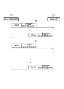
forming device and a memory unit provided in the consumable unit communicate
with
each other. However, there are numerous variables in the communication
process. For
instance, there may be an attack by a hacker who tries to control the
controller or the
memory unit for malicious purposes.
[10] In addition, there may be a noise interruption caused, for example, by
an electronic
circuit or a motor provided in an image forming device. Unexpected incidents
such as
an alien substance getting into a connection part between a main body and a
consumable unit of an image forming device, a connection cutting off due to
vibration
during operations, and/or an electrical interference signal being applied
through the
connection part, may occur.
[11] Communication data may change due to these variables. For instance,
once a job is
completed, a consumable unit may transmit information such as the number of
printing
pages, number of dots, and remaining toner volume to a controller, and copies
the in-
formation to a nonvolatile memory of the controller. Upon the data being read
as an
incorrect value, for example, such as OxFFFFFFFF, there is a risk that the
controller
may perceive that the life of the pertaining consumable unit has ended. In
this case, the
consumable unit will not longer be able to be used.
[12] In addition, the consumable unit of an image forming device may have a
structure
that may be detachable. A memory of a consumable unit is not usually accessed
and
only the memory of an image forming device is used during a printing operation
of the
image forming device due, for example, to motor vibration and circuit noise
that may
occur during the operation. Thus, the communication between the memory of the
consumable unit and the image forming device may be performed only in limited
occasions, for example, when the consumable unit is mounted on the image
forming
device so that the memory of the consumable unit and the memory of the image
forming device are synchronized with each other, or when the consumable unit
is
updated for changes after a printing operation is completed and a motor stops.
CA 02896345 2015-06-23
WO 2014/104511 PCT/ICR2013/006430
[13] As there may be a considerable amount of data stored and managed in
the
consumable unit, various supplementary functions may be required, taking a
prolonged
communication time. Accordingly, when a consumable unit is replaced during
commu-
nication, problems may occur. As an example, a consumable usage information of
a
consumable unit 1 indicates, for example, 100 printing pages, 200 output dots,
and 300
motor driving times, and a consumable usage information of a consumable unit 2
indicates, for example, 200 printing pages, 300 output dots, and 400 motor
driving
times. In this example case, if the consumable unit 1 is mounted on an image
forming
device, the consumable unit 1 may be synchronized with the memory and data of
the
image forming device. If the consumable unit 1 is replaced with the consumable
unit 2
in the process of synchronization, that is, only the data of 100 printing
pages and 200
output dots of the consumable unit 1 is stored in the memory of the image
forming
device and then, the consumable unit 1 is replaced with the consumable unit 2,
authen-
tication may be performed again. Subsequently, the data of 400 motor driving
time
may be copied to the memory of the image forming device. As a result, the
memory of
the image forming device indicates, for example, 100 printing pages, 200
output dots,
and 400 motor driving times, which are not the correct values. In this example
case, if
the consumable unit 2 is updated for changes after a printing operation is
completed in
the image forming device, the data of 100 printing pages and 200 output dots
stored in
the memory of the image forming device may be stored in the consumable unit 2
while
the actual data of the consumable unit 2 indicates 200 printing pages and 300
output
dots. As the printing pages become 100 instead of 200, the corresponding
consumable
unit has incorrect data values and thus, may cause problems.
[14] In addition, an image forming device may have and use a plurality of
consumable
units in one Inter-Integrated Circuit (I2C) channel, in which case, the
consumable units
may be categorized by a slave address in the I2C channel. In this case, if a
slave
address is modified to the ID of another consumable unit due to some temporal
problems, wrong data may be stored in the memory of the another consumable
unit.
[15] Further, regarding a consumable unit of which the life span has ended,
a hacker may
attempt to reset the consumable user information, for example, to a value of
"0" with a
malicious purpose, in order to inappropriately recycle the consumable unit. Ac-
cordingly, a user may attempt to use a consumable unit of which the life has
ended,
causing problems such as breakdown of the image forming device or
deterioration of
definition, and the user may not be provided with exact information regarding
consumable units, and moreover, an integrated solution service may not be
available
due to the problems of MPS caused by incorrect consumable information.
Disclosure of Invention
4
CA 02896345 2015-06-23
WO 2014/104511 PCT/ICR2013/006430
Technical Problem
[16] Accordingly, the necessity for a technology which efficiently detects
communication
errors between a consumable unit, and an image forming device to seek safety
of the
data is required.
Solution to Problem
[17] Additional aspects and/or advantages will be set forth in part in the
description which
follows and, in part, will be apparent from the description, or may be learned
by
practice of the invention.
[18] An aspect of an exemplary embodiments relates to a CRUM chip and an
image
forming device for safety of communication, using integrity detection data,
and a com-
munication method thereof.
[19] An image forming apparatus according to an exemplary embodiment
includes a main
body that includes a main controller capable of controlling operations of the
image
forming apparatus, a consumable unit that is mounted on the main body to com-
municate with the main controller, and a Customer Replaceable Unit Monitoring
(CRUM) chip that is provided in the consumable unit and stores information
regarding
the consumable unit, and the main controller and the CRUM chip perform data
com-
munication if authentication is successful, wherein the authentication is
performed
through a plurality of authentication processes, and integrity detection data
which is
generated by reflecting previous integrity detection data is used in at least
two authen-
tication processes from among the plurality of authentication processes.
[20] The main controller and the CRUM chip may generate final integrity
detection data
by accumulatively reflecting all integrity detection data that has been
transmitted or
received in previous authentication processes in a final authentication
process from
among the plurality of authentication processes.
[21] The main controller and the CRUM chip may transmit/receive a signal
including the
integrity detection data in an authentication process for generating a session
key and an
authentication process for verifying compatibility from among the plurality of
authen-
tication processes.
[22] The main controller and the CRUM chip may perform at least one
authentication
process between the authentication process for generating a session key and
the au-
thentication process for verifying compatibility.
123] When the authentication process for generating a session key begins,
the main
controller may transmit a signal including first data and first integrity
detection data to
the CRUM chip, and the CRUM chip may generate second integrity detection data
using second data and the first integrity detection data and transmit a signal
including
the second data and the second integrity detection data to the main
controller, and each
5
CA 02896345 2015-06-23
WO 2014/104511 PCT/ICR2013/006430
of the first data and the second data may include data related to a session
key in order
to generate a session key.
[24] When the authentication process for verifying compatibility begins,
the main
controller may generate third integrity detection data using third data, the
first integrity
data and the second integrity data and transmit a signal including the third
data and the
third integrity detection data to the CRUM chip, the CRUM chip may generate
fourth
integrity detection data using fourth data, and the first to the third
integrity detection
data and transmit a signal including the fourth data and the fourth integrity
detection
data, and the third data may include index information in a table pre-stored
in the
image forming apparatus, and the fourth data may include a value corresponding
to the
index information.
[25] Each of the main controller and the CRUM chip, when a signal including
the
integrity detection data is received from a counterpart, may separate the
integrity
detection data from the received signal and compare the separated integrity
detection
data with integrity detection data which is generated on its own from
remaining data in
order to verify integrity of the signal.
[26] An image forming apparatus according to an exemplary embodiment
includes an
interface unit that is connected to a CRUM chip mounted on a consumable unit
built in
the image forming apparatus and a controller which, when an event where authen-
tication is required occurs, authenticates the CRUM chip by performing a
plurality of
authentication processes of the CRUM chip, and the controller
transmits/receives a
signal including integrity detection data in an authentication process for
generating a
session key and an authentication process for verifying compatibility from
among the
plurality of authentication processes, and the integrity detection data is
generated by
accumulatively reflecting at least one integrity detection data included in a
previously-
received signal.
127] A CRUM chip mountable on a consumable unit of an image forming
apparatus
according to an exemplary embodiment includes an interface unit which receives
a
signal including first data and first integrity detection data regarding the
first data from
a main body of the image forming apparatus, a test unit which separates the
first
integrity detection data from the received signal in order to verify integrity
of the
signal, a generating unit which generates second integrity detection data
using second
data for authentication with a main body of the image forming device and the
first
integrity detection data, and a controller which performs authentication by
transmitting
a signal including the second data and the second integrity detection data to
a main
body of the image forming device through the interface unit.
[28] Each of the first data and the second data may include data related to
a session key in
order to generate a session key, and the controller may generate the session
key using
6
CA 02896345 2015-06-23
WO 2014/104511 PCT/ICR2013/006430
the first data and the second data, and perform a plurality of subsequent
authentication
processes,
[29] The plurality of subsequent authentication processes may comprise a
second authen-
tication process for synchronizing a first table stored in each of a main body
of the
image forming device and the CRUM chip, a third authentication process for syn-
chronizing a second table stored in each of the main body of the image forming
device
and the CRUM chip, and a fourth authentication process for determining
compatibility
between the image forming device and the CRUM chip based on at least one of
the
first and the second tables.
[30] The controller may generate and transmit final integrity detection
data by reflecting
all integrity detection data which has been transmitted and received in the
fourth au-
thentication process.
[31] A method for authenticating an image forming apparatus according to an
exemplary
embodiment includes determining whether an event that requires authentication
of a
consumable unit mounted on the image forming device occurs, and upon the event
occurring, performing authentication of a CRUM chip mounted on the consumable
unit
by a main controller of the image forming device to authentication the CRUM
chip,
and the authentication is performed through a plurality of authentication
processes, and
integrity detection data generated by reflecting previous integrity detection
data is used
in at least two authentication processes from among the plurality of
authentication
processes.
[32] Integrity detection data which is transmitted/received in a final
authentication process
from among the plurality of authentication processes may be generated by
accumu-
latively reflecting all integrity detection data which has been transmitted or
received in
previous authentication processes.
[33] The authenticating may comprise a first authentication operation in
which the main
controller transmits a signal including first data and first integrity
detection data to the
CRUM chip, and the CRUM chip generates second integrity detection data using
second data and the first integrity detection data and transmits a signal
including the
second data and the second integrity detection data to the main controller and
a second
authentication operation in which the main controller generates third
integrity detection
data using third data, the first integrity detection data and the second
integrity detection
data and transmits a signal including the third data and the third integrity
detection data
to the CRUM chip, and the CRUM chip generates fourth integrity detection data
using
fourth data and the first to the third integrity detection data and transmits
a signal
including the fourth data and the fourth integrity detection data to the main
controller,
wherein each of the first data and the second data includes data related to a
session key
in order to generate a session key, wherein the third data includes index
information in
7
CA 02896345 2015-06-23
WO 2014/104511 PCT/ICR2013/006430
a table pre-stored in the image forming apparatus, and the fourth data
includes a value
corresponding to the index information
[34] A method for authenticating a CRUM chip mountable on a consumable unit
of an
image forming apparatus according to an exemplary embodiment includes
receiving a
signal including first data and first integrity detection data for
authentication from a
main body of the image forming apparatus, testing integrity of the signal by
separating
the first integrity detection data from the received signal, generating second
integrity
detection data using second data and the first integrity detection data for
authentication
with a main body of the image forming apparatus, and performing authentication
by
transmitting a signal including the second data and the second integrity
detection data
to a main body of the image forming apparatus.
[35] The method may include performing a plurality of subsequent
authentication
processes after transmitting a signal including the second data and the second
integrity
detection data to a main body of the image forming apparatus, and integrity
detection
data which is transmitted/received in a final authentication process from
among the
plurality of subsequent authentication processes may be generated by
accumulatively
reflecting all of integrity detection data which is transmitted or received in
previous au-
thentication processes.
[36] The final authentication process may include receiving third data, the
first integrity
detection data and a signal including third integrity detection data generated
using the
second integrity detection data and the third data from a main body of the
image
forming apparatus, and generating fourth data and fourth integrity detection
data using
the first to the third integrity detection data and transmitting a signal
including the
fourth data and the fourth integrity detection data to a main body of the
image forming
apparatus, and each of the first data and the second data may include data
related to a
session key in order to generate a session key, and the third data may include
index in-
formation in a table pre-stored in the image forming apparatus, and the fourth
data may
include a value corresponding to the index information.
[37] An image forming device according to an exemplary embodiment includes
a main
body that includes a main controller capable of controlling operations of the
image
forming apparatus, and a consumable unit where a Customer Replaceable Unit
Monitoring (CRUM) chip is mounted, and the main controller, when an event
where
authentication of the CRUM chip is required occurs, transmits a first signal
including
first data and first integrity detection data to the CRUM chip, and the CRUM
chip
generates second integrity detection data using second data and the first
integrity
detection data and transmits the second data and a second signal including the
second
data and the second integrity detection data to the main controller in order
to perform
an authentication process to generate a session key, and the main controller
transmits a
8
third signal including third integrity detection data and the third data which
is generated
using the first integrity detection data and the second integrity detection
data to the
CRUM chip, generates fourth integrity detection data using the first to the
third
integrity detection data, and transmits a fourth signal including the fourth
data and the
fourth integrity detection data to the main controller in order to perform an
authentication process to detemiine compatibility.
[38] The first data may include a first command, first authentication data,
and a first
assignor for assigning the first integrity detection data, and the second data
may include
second authentication data and a second assignor for assigning the second
integrity
detection data based on an operation result according to the first command,
the third
data may include a second command, third authentication data, and a third
assignor for
assigning the third integrity detection data, and the fourth data may include
fourth
authentication data and a fourth assignor for assigning the fourth integrity
detection
data based on an operation result according to the second command.
[38a] A Customer Replaceable Unit Monitoring (CRUM) chip operable to
communicate
with an image forming device according to an exemplary embodiment comprises:
an
interface including at least one contact and operable to receive first data
and first
integrity detection data regarding the first data that is transmitted from a
main
controller of the image folluing device; and a controller that is operable to:
generate
second integrity detection data using both second data to be transmitted to
the main
controller of the image forming device and the first integrity detection data;
and
transmit the second data and the second integrity detection data from the CRUM
chip to
the main controller of the image forming device.
[38b] An authentication method of a Customer Replaceable Unit Monitoring
(CRUM) chip
operable to communicate with an image forming device according to an exemplary
embodiment comprises: receiving, by the CRUM chip, first data and first
integrity
detection data regarding the first data from a main controller of the image
forming
device; generating second integrity detection data using both second data and
the first
integrity detection data; and transmitting, from the CRUM chip, the second
data and the
second integrity detection data to the main controller of the image forming
device.
[38c] A consumable apparatus according to an exemplary embodiment
comprises: a
consumable unit that is mounted on an image forming device; and a Customer
Replaceable Unit Monitoring (CRUM) chip, wherein the CRUM chip comprises: an
CA 2896345 2018-06-15
8a
interface including at least one contact and operable to receive first data
and first
integrity detection data regarding the first data that is transmitted from a
main
controller of the image forming device; and a controller that is operable to:
generate
second integrity detection data using both second data to be transmitted to
the main
controller of the image forming device and the first integrity detection data;
and
transmit the second data and the second integrity detection data from the CRUM
chip to
the main controller of the image forming device.
Advantageous Effects of Invention
[39] As aforementioned, according to various exemplary embodiments of the
present
disclosure, it is possible to pursue safety of an entire communication by
accumulatively
using integrity detection data used in previous communications. Accordingly,
information of consumable units and image forming devices can be managed
safely.
Brief Description of Drawings
[40] The above and/or other aspects of the present disclosure will be more
apparent by
describing certain present disclosure with reference to the accompanying
drawings, in
which:
[41] FIG. 1 illustrates an image forming device according to an exemplary
embodiment;
[42] FIG. 2 is a timing view illustrating a communication process between a
controller and
a CRUM chip in an image forming device according to an exemplary embodiment;
[43] FIG. 3 is a timing view illustrating a process of examining integrity
of a signal using
an integrity detection data;
[44] FIG. 4 is a timing view illustrating a communication process between a
controller and
a CRUM chip in an image forming device according to an exemplary embodiment;
[45] FIG. 5 is a block diagram illustrating an exemplary image forming
device mounted
on a consumable unit;
[46] Figs. 6 and 7 an exemplary image forming device according to various
exemplary
embodiments;
[47] FIG. 8 illustrates a configuration of a CRUM chip according to an
exemplary
embodiment of the present disclosure;
[48] Figs. 9 and 10 illustrate a communication method according to various
exemplary
CA 2896345 2018-06-15
9
CA 02896345 2015-06-23
WO 2014/104511 PCT/ICR2013/006430
embodiments
[49] FIGS. 11 to 18 are views illustrating an authentication method of an
image forming
device according to an exemplary embodiment;
[50] FIG. 19 is a block diagram illustrating a configuration of a CRUM chip
according to
an exemplary embodiment;
[51] FIG. 20 is a timing view illustrating an authentication process;
[52] FIGS. 21 to 24 illustrates an exemplary method for generating
integrity detection
data used for each authentication process;
[53] FIGS. 25 to 27 illustrating an exemplary connecting a consumable unit
to a main
body of an image forming apparatus;
[54] FIG. 28 illustrating an exemplary wave form of a signal which is
transmitted and
received according to an I2C interface method; and
[55] FIG. 29 is a view magnifying in exemplary part of the signal in FIG.
28.
Mode for the Invention
156] Reference will now be made in detail to the embodiments, examples of
which are il-
lustrated in the accompanying drawings, wherein like reference numerals refer
to the
like elements throughout. The embodiments are described below to explain the
present
invention by referring to the figures.
[57] Exemplary embodiments are discussed in detail below with reference to
the ac-
companying drawings.
[58] In the following description, like drawing reference numerals are used
for the similar
elements. The matters defined in the description, such as detailed
construction and
elements, are provided to assist in a comprehensive understanding of exemplary
em-
bodiments.
[59] FIG. 1 illustrates a configuration of an image forming device
according to an
exemplary embodiment. As illustrated in FIG. 1, for example, an image forming
device
includes a body 100, a controller 110 provided in the body 100, and a
consumable unit
200 that can be mounted on the body 100. An image forming device can be
embodied
as various types of devices such as a printer, scanner, multi-function device,
facsimile,
or copy machine, which can form images on paper or on other various recording
media. According to an exemplary embodiment the body 100 may be a main body of
the image forming device and the controller 110 may be a main controller.
[60] The controller 110 may be mounted on the body 100 of the image forming
device to
control functions of the image forming device. According to an exemplary em-
bodiment, the controller 110 is a main controller that controls all functions
of the
image forming device.
161] The consumable unit 200 may be mounted on the body 100 of the image
forming
10
CA 02896345 2015-06-23
WO 2014/104511 PCT/ICR2013/006430
device, and can be one of various types of units which involve in the image
forming
device either directly or indirectly. For instance, in the case of a laser
image forming
device, electrification units, light exposure units, developing units,
transfer units,
settlement units, various types of rollers, belts, and OPC drums can be
consumable
units. Furthermore, various types of units that must be replaced in using an
image
forming device can be defined as a consumable unit 200.
[62] Each consumable unit 200 may have a predetermined life span.
Therefore, a
consumable unit 200 may include a microprocessor and/or circuit such as a CRUM
chip (Customer Replaceable Unit Monitoring chip) 210 which enables replacement
at
an appropriate time.
[63] A CRUM chip 210 may be mounted on a consumable unit 200 and record
various in-
formation. A CRUM chip 210 includes a memory. Therefore, a CRUM chip 210 may
be referred to in various terms such as a memory unit, or CRUM memory
(Customer
Replaceable Unit Monitoring memory), but for the sake of convenience of
explanation,
the term "CRUM chip" will be used.
[64] In the memory provided in the CRUM chip, various characteristics
information
regarding the consumable unit 200, the CRUM chip itself, or the image forming
device, and also usage information or programs regarding conducting an image
forming job may be stored.
[65] Various programs stored in the CRUM chip may include not only general
ap-
plications, but also 0/S (Operating System) programs and encryption programs.
In-
formation on the manufacturer of the consumable unit 200, information on manu-
facturer of the image forming device, names of mountable image forming
devices, in-
formation on the manufactured date, serial number, model name, electronic
signature
information, encryption key, and encryption key index may be included in the
charac-
teristics information. The usage information may include information such as
how
many sheets of paper have been printed so far, how many sheets of paper can be
printed from now on, and how much toner is left. The characteristics
information may
also be referred to as unique information instead.
[66] According to an exemplary embodiment, information as illustrated below
in Table 1
can be stored in a CRUM chip 210.
[67] Table 1
11
CA 02896345 2015-06-23
WO 2014/104511 PCT/ICR2013/006430
[Table 11
General Information
OS VersionSPL-C VersionEngine CLP300_V1.30.12.35 02-22-20075.24
VersionUSB Serial NumberSet Mod- 06-28-20066.01.00(55)BH45BAIP914466
elService Start Date B.D0M2007-09-29
Option
RAM SizeEEPROM SizeUSB Connected 32 Mbytes4096 bytes
(High)
Consumables Life
Total Page CountFuser LifeTransfer 774/93 Pages (Color/mono)1636
Roller LifeTrayl Roller Life Pages864 Pages867 Pages
Total Image CountImaging Unit/Deve 3251 Images61 Images/19 Pages3251
Roller LifeTransfer Belt LifeToner Image Images14/9/14/19 Images(C/M/Y/K)
Count
Toner Information
Toner Remains PercentToner Average 99%/91%/92%/100%
Coverage (C/M/Y/K)5%/53%/31%/3% (C/M/Y/K)
Consumables Information
Cyan TonerMagenta TonerYellow SAMSUNG(DOM)SAMSUNG(DOM)SA
TonerBlack TonerImaging unit MSUNG(DOM)SAMSUNG(DOM)SAM
SUNG(DOM)
Color Menu
Custom Color Manual Adjust (CMYK : 0,0,0,0)
Setup Menu
Power SaveAuto ContinueAltitude Adj. 20 MinutesOnPlain
[68] In the memory of the CRUM chip 210, approximate information of the
consumable
unit 200, and information on the life, information, and setup menu of the
consumable
unit 200 may be stored. Besides the body of the image forming device, an 0/S
provided for use in the consumable unit may be stored in the memory.
[69] The CRUM chip may include a CPU (not illustrated) that can manage the
memory,
perform various programs stored in the memory, and perform communication with
a
body of an image forming device or a controller of other devices.
[70] The CPU may drive the 0/S stored in the memory of the CRUM chip, and
perform
initialization of the consumable unit 200 itself, apart from the
initialization of the
12
CA 02896345 2015-06-23
WO 2014/104511 PCT/ICR2013/006430
image forming device. The CPU may perform authentication between the body of
the
image forming device when the initialization has completed or during the
initialization.
Once the initialization is complete, it may perform encryption data
communication
with the body of the image forming device. Various commands and data
transmitted
from the body of the image forming device may be encrypted according to an
arbitrary
encryption algorithm and be transmitted.
[71] In a particular event, for example. such as when power of the image
forming device
having the consumable unit 200 is on, or when the consumable unit 200 is
detached
and then attached to the body 100 of the image forming device again, the CPU
may
perform initialization for itself apart from the initialization of the
controller 100. The
initialization includes various processes such as initial driving of various
application
programs used in the consumable unit 200, calculating secret information
needed in
data communication with the controller 110 after the initialization, setting
up a com-
munication channel, initializing a memory value, checking when to replace
itself,
setting an inner register value of the consumable unit 200, and setting a
inner-outer
clock signal.
[72] Setting a register value may be defined as an operation of setting
functional register
values inside the consumable unit 200 so that the consumable unit 200 can
operate
according to various functional states that a user predetermined. The setting
an inner-
outer clock signal refers to an operation of adjusting a frequency of an outer
clock
signal provided from the controller 110 of the image forming device to be in
line with
the inner clock signal that the CPU inside the consumable unit 200 uses.
[73] Checking when to replace itself may be an operation of identifying the
remaining
volume of a toner or ink used so far, anticipating when the ink or toner will
run out,
and notifying the controller 110. Upon determining in the initialization
process that the
toner volume has already run out, the consumable unit 200 may be embodied to
notify
the controller 110 that it is in a non-operable state. Since the consumable
unit 200 itself
has the 0/S, various types of initialization may be performed according to the
types
and characteristics of the consumable unit 200.
[74] Upon the CPU being mounted and the 0/S provided, the remaining volume
of the
consumable unit stored in the memory unit 210 may be identified or the number
of
refilling times, before the controller 110 requests communication with the
unit 200,
when the image forming device is turned on. Accordingly, the time of notifying
shortage of the consumable unit may be done earlier than before. For instance,
when
the toner is running short, a user may turn the power on, and then make
adjustments for
conversion to a toner saving mode and then perform image forming. The same
applies
to when only a particular toner is running short as well.
[75] The CPU may not respond to a command of the controller 110 until the
initialization
13
CA 02896345 2015-06-23
WO 2014/104511 PCT/ICR2013/006430
is under process and then completed. The controller 110 waits for a response
while pe-
riodically transmitting the command until there is a response.
[76] Accordingly, when a response, that is, an acknowledgement is received,
authen-
tication may be performed between the controller 110 and the CPU. In this
case, due to
the 0/S of itself installed in the CRUM chip 210, it is possible to perform
authen-
tication through interaction between the CRUM unit 210 and the controller 110.
[77] The controller 110 encrypts data or a command for authentication and
transmits it to
the CRUM chip 210. In the transmitted data, an arbitrary value R1 may be
included.
Herein, the R1 may be a random value which changes at every authentication, or
a pre-
determined fixed value. The CRUM chip that received the data generates a
section key
using an arbitrary value R2 and the received R1, and then generates an MAC
(Message
Authentication Code) using the generated section key.
[78] A signal including the MAC generated and the R2 as aforementioned is
transmitted
to the controller 110. The controller 110 generates the section key using the
received
R2 and R1, generates the MAC using the generated section key, and then
certifies the
CRUM chip 210 by comparing the generated MAC and the MAC in the received
signal. According to various exemplary embodiments, electronic signature
information
or key information may be transmitted in such an authentication process and
used in
the authentication.
[79] Once authentication is made successfully, the controller 110 and the
CRUM chip
perform an encryption data communication for data management. That is, when a
user
command has been input or when an image forming job has been initiated or
completed, the controller 110 encrypts the command or data for performing data
reading, writing, or additional functions using an encryption algorithm, and
then
transmits it to the CRUM chip 210.
[80] The CRUM chip 210 may decode the received command or data, and perform
op-
erations such as data reading or writing corresponding to the decoded command.
The
encryption algorithm used in the CRUM chip 210 or the controller 110 may be a
stan-
dardized encryption algorithm. Such an encryption algorithm is changeable when
the
encryption key has been leaked or when there is a need to strengthen security.
Various
encryption algorithms such as RSA asymmetric key algorithm, ARIA, TDES, SEED,
AES symmetric key algorithm may be used.
[81] As such, between the CRUM chip 210 and the controller 110,
communication for au-
thentication and data exchange may be performed numerous times. In every commu-
nication, signals are transmitted from the controller 110 to the CRUM chip 210
or vice
versa. In this case, a transmitted signal includes error detection data for
detecting
integrity of the data included in the corresponding signal. Such error
detection data is
data generated by accumulation of error detection data included in the
transmitted or
14
CA 02896345 2015-06-23
WO 2014/104511 PCT/ICR2013/006430
received signal from the previous communication.
[82] That is, between the controller 110 and the CRUM chip 210, a plurality
of commu-
nications may be performed such as authentication 1, authentication 2,
authentication
3, ..., authentication n, data communication 1, data communication 2. ...,
data commu-
nication m. According to an exemplary embodiment, in a signal transmitted at
every
communication or in some process of the communication, integrity detection
data may
be included. In such an integrity detection data, the integrity detection data
used in the
previous communication is reflected accumulatively.
[83] The side that received the signal detects integrity of the
corresponding signal using
integrity detection data in the signal. Accordingly, when the corresponding
data is de-
termined to be integral, a next operation or subsequent communication is
performed. If
it is necessary to record the received data, the data and integrity detection
data included
in that signal may be temporarily stored. A new integrity detection data may
be
generated using a subsequent data to be transmitted to the side which
transmitted the
signal and the integrity detection data received from the previously
communication and
temporarily stored. Accordingly, a signal to which the new integrity detection
data has
been added may be transmitted to the subsequent data. Between the controller
110 and
the CRUM chip 210, such communication which includes such integrity detection
data
may be performed a plurality of times. When the communication including the
last
integrity detection data is performed, a final detection may be performed
using the
integrity detection data included in the last signal received. If there is
nothing wrong
with the final detection, all data which has been temporarily stored until
then may be
recorded.
[84] FIG. 2 illustrates an exemplary communication process between the
controller 110
and the CRUM chip 210 according to an exemplary embodiment of the present
disclosure. According to FIG. 2, the controller 110 transmits a first signal
10 which
includes data 1 and integrity detection data 1. The CRUM chip 210 which
received the
first signal 10 generates integrity detection data 2 using the integrity
detection data 1
included in the first signal 10 and data 2. The CRUM chip 210 transmits a
second
signal which includes the data 2 and the integrity data 2 to the controller
110. As such,
the signals (30, ..., N) which include integrity detection data generated
using the
integrity detection data from the previous communication are performed for a
plurality
of times.
185] A result value of logical calculus on data to be transmitted, a result
value generated
by applying a predetermined mathematically formula to the data or a result
value of en-
crypting the data, that is, MAC may be used as integrity detection data.
[86] FIG. 3 illustrates a detection method using integrity detection data.
According to
FIG. 3, when a signal which includes data a and integrity detection data a is
received
15
CA 02896345 2015-06-23
WO 2014/104511 PCT/ICR2013/006430
(S310), the CRUM chip 210 separates the integrity detection data a (S320).
[87] The CRUM chip 210 generates integrity detection data a' using the
remaining data
and integrity detection data that it had transmitted during the previous
communication
(S330). The CRUM chip 210 then compares the integrity detection data a
generated ac-
cordingly with the separated integrity detection data a (S340), and if they
are identical,
determines to be integral (S350). If they are not identical, the CRUM chip 210
de-
termines that the data is in an error state, and stops the communication
(S360). For the
convenience of explanation, hereinafter, the integrity detection data a' will
be referred
to as the data subject to comparison.
[88] When it is determined that the corresponding data is integral,
integrity detection data
b is generated by using data b to be transmitted and the detection data a
(S370). Ac-
cordingly, a signal which includes the data b and the integrity detection data
b is
transmitted to the controller 110 (S380).
[89] FIG. 3 illustrates an exemplary detection process performed, for
example, in the
CRUM chip 210, but the same process may be performed in the controller 110 as
well.
That is, when the controller 110 receives a signal which includes the data b
and the
integrity detection data b, it separates the integrity detection data b, and
performs
detection. This detection method is similar to (S330) to (S370), and thus
repeated ex-
planation and illustration will be omitted.
[90] The configuration of signals transmitted and received between the
controller 110 and
the CRUM chip 210 may be designed in various types. That is, data included in
the
signals may include at least one of a command, information to be recorded,
result in-
formation on operations according to the command, result information on
integrity
detection regarding previously received signals, and indicator information for
notifying
a location of the integrity detection data. The result information on
integrity detection
may be excluded from the signals initially transmitted and received between
the
controller 110 and the CRUM chip 210. The method for detecting integrity data
may
be used for every communication operation in the above communication process,
but
may also be applied only to some or important communication operations during
the
entire communication process, if necessary.
[91] FIG. 4 illustrates an exemplary embodiment of a process of detecting
integrity using
signals having different formats, for example, different from those of FIG. 2.
According to FIG. 4, the controller 110 transmits a signal which includes data
and
integrity detection data 1 (S410). Herein, the data includes a Read Command
(CMD)
data 1 and an indicator Ul. The Read Command(CMD) data 1 includes not only a
command but also a read target or a memory address. The Ul refers to indicator
in-
formation which follows the Read Command(CMD) data 1. The indicator
information
Ul refers to a symbol for notifying a location of parsing of the integrity
detection data
16
CA 02896345 2015-06-23
WO 2014/104511 PCT/ICR2013/006430
in the signal. The indicator information may be expressed as fixed number of
bites. For
example, five bytes may be used for the indicator information. On the other
hand, the
Read Command(CMD) data 1 is variable according to the contents of the data,
and
thus the size of the integrity detection data 1 is also variable.
[92] When the signal is received, the CRUM chip 210 performs integrity
detection using
the integrity detection data 1 included in the signal (S415). The CRUM chip
210 is
capable of generating integrity detection data 2 using the data to be
transmitted and the
integrity detection data 1, and transmits the signal which includes these
(S420). As il-
lustrated in FIG. 4, in the signal to be transmitted, a Read data 1 which is
data read
from the memory provided in the consumable unit 100 according to the Read
Command(CMD) data 1, a Result data 2 which indicates the result of operation
performed according to the Read Command(CMD) data 1, an indicator U2, and an
integrity detection data 2 are included.
[93] The controller 110 separates the integrity detection data 2 from the
received signal
and performs integrity detection (S425). Then, if there exists a subsequent
Read
Command(CMD) data 3, the controller 110 generates an integrity detection data
3
using the Read Command(CMD) data 3 and the integrity detection data 2, and
then
transmits a signal which includes the Read Comrnand(CMD) data 3, an indicator
U3,
and an integrity detection data 3 to the CRUM chip 210 (S430).
[94] As illustrated in FIG. 4, for example, communications using a
plurality of integrity
detection data 4, 5, 6, Ti, and T2 are performed (S440, S450, S460, S470,
S485),
followed by integrity detections accordingly (S435, W445, S455, S465). When
the
final communication signal is received from the CRUM chip 210 (S470), the CRUM
chip 210 detects integrity of the data which have been transmitted and
received in the
entire communication process and temporarily stored using integrity detection
data T1
included in the final communication signal (S475). If it is determined that
the data is
integral as a result of the final detection, the data which has been
temporarily stored is
stored in a non-volatile memory (not illustrated) (S480). Likewise, when the
final com-
munication signal is transmitted from the CRUM chip 210, the controller 110
also
performs the entire integrity detection using the integrity detection data T2
included in
the final communication signal (S490). Accordingly, the data which has been
tem-
porarily stored is stored in the non-volatile memory, if it is determined that
the data is
integral (S495).
195] The integrity detection data used in such communication processes is
generated by
accumulating integrity detection data used in the previous communications.
[96] According to an exemplary embodiment, the integrity detection data may
be
processed as follows:
[97] Integrity detection data 1 = E(Read CMD Data 1 U1)
17
CA 02896345 2015-06-23
WO 2014/104511 PCT/ICR2013/006430
198] Integrity detection data 2 = E(Read CMD Data 2 Result Data 2 U2
Integrity
detection data 1)
[99] Integrity detection data 3 = E(Read CMD Data 3 U3 Integrity detection
data 2)
[100] Integrity detection data 4 = E(Read CMD Data 4 Result Data 4 U4
Integrity
detection data 3)
[101]
Integrity detection data 5 = E(Write CMD Data 5 U5 Integrity detection data
4)
[102] Integrity detection data 6 = E(Read Data 6 U6 Integrity detection
data 5)
11031 Integrity detection data Ti = E(Write CMD Data Li U-Ti Integrity
detection
data T1-1)
[104] Integrity detection data T2 = E(Result Data L2 U-T2 Integrity
detection data
Ti)
[105] In the aforementioned formulas, the term "E( )" indicates a function
of applying a
predetermined formula to obtain a result value. As such, integrity detection
data may
be generated from adding the previous integrity detection data and the entire
data to be
transmitted, applying various logical calculus such as X0R(eXclusive OR), from
resulting value of substituting data into other known formulas between the
controller
110 and the CRUM chip 210, and from resulting value of encryptions by applying
various aforementioned various encryption algorithms.
[106] FIG. 5 illustrates an exemplary image forming device where a
plurality of
consumable units 200-1, 200-2, ..., 200-n are provided within the body 500
according
to an exemplary embodiment of the present disclosure.
[107] As illustrated in FIG. 5, an image forming device includes a
controller 510, a user
interface unit 120, an interface unit 130, a memory unit 140, and a plurality
of
consumable units 200-1, 200-2, ... 200-n.
[108] The user interface unit 120 performs a role of receiving various
commands from the
user, or showing and notifying various information. The user interface unit
120 may
include an LCD or LED display, at least one button, or a speaker. It may also
include a
touch screen depending on circumstances.
[109] The interface unit 130 refers to a configuration which may be
connected with a wired
connection and/or wirelessly with a host PC or various external devices to
perform
communication. The interface unit 130 may include various types of interfaces
such as
a local interface, USB (Universal Serial BUS) interface, and a wireless
network
interface.
11101 The memory unit 140 performs a role of storing various programs or
data necessary
for driving the image forming device.
[111] The controller 510 performs a role of controlling the entire
operations of the image
forming device. The controller 510 processes data received through the
interface unit
130, and converts the processed data into a format in which image can be
formed.
18
CA 02896345 2015-06-23
WO 2014/104511 PCT/ICR2013/006430
11121 The controller 510 performs an image forming job on the converted
data using a
plurality of consumable units 200-1, 200-2, ..., 200-n. The consumable unit
may be
provided in various ways depending on the type of the image forming device.
[113] In the case of a laser printer, electrification units, light exposure
units, developing
units, transfer units, settlement units, various types of rollers, belts, and
OPC drums
can be consumable units.
[114] In each consumable unit 200-1, 200-2, ..., 200-n, a first CRUM chip
to n CRUM chip
210-1, 210-2, ..., 210-n may be included.
[115] Each CRUM chip may include a memory and CPU etc. At least one of a
crypto
module, tamper detector, interface unit, clock unit (not illustrated) which
outputs clock
signals, or random value generating unit (not illustrated) which generates a
random
value for authentication may be included.
[116] The crypto unit (not illustrated) supports the encryption algorithm
so that the CPU
(not illustrated) can perform authentication or encrypted communication with
the
controller 510. The crypto unit may support a determined algorithm among a
plurality
of encryption algorithms such as RSA, ECC asymmetric key algorithm and ARIA,
TDES, SEED, and AES symmetric key algorithm. The controller 510 may also
support
a corresponding algorithm among a plurality of encryption algorithms.
Accordingly,
the controller 510 may identify what kind of encryption algorithm is used in
the
consumable unit 200, proceed with the encryption algorithm, and perform
encryption
communication.
[117] Consequently, even when a key is issued, regardless of the kind of
encryption
algorithm applied to the consumable unit 200, the key may be easily mounted on
the
body 100 and perform encryption communication.
[118] A tamper detector (not illustrated) is a unit for defending various
physical hacking
attempts, that is, tampering .A tamper detector monitors an operation
environment such
as voltage, temperature, pressure, light, and frequency, and when there is an
attempt
such as decap, either erases or physically blocks data. In this case, the
tamper detector
may have a separate power.
[119] The memory provided inside the CRUM chip 210 may include an 0/S
memory, non-
volatile memory, or volatile memory. The 0/S memory (not illustrated) may
store the
0/S for driving the consumable unit 200. The non-volatile memory (not
illustrated)
may store various data non-volatility. In the non-volatile memory, various
information
such as electronic signature information, various encryption algorithm
information, in-
formation on the state of the consumable unit 200 (for instance, the remaining
toner
volume, when to exchange the toner, the remaining number of printing sheets
etc.),
unique information (for instance, manufacturer information, manufacturing date
in-
formation, serial number, model name of the product etc.), and A/S information
may
19
CA 02896345 2015-06-23
WO 2014/104511 PCT/ICR2013/006430
be stored. Data received in the process of communication with the controller
may be
stored in the non-volatile memory.
[120] The volatile memory (not illustrated) may be used as a temporary
storage space
needed for operation. In the volatile memory, the data determined to be
integral in
every communication and the integrity detection data used in each
determination may
be temporarily stored.
[121] The interface unit (not illustrated) takes a role of connecting the
CPU with the
controller and may be embodied as a serial interface or a wireless interface.
Since the
serial interface uses a smaller number of signals than a parallel interface,
it has a cost
saving effect, and further, it is appropriate in operation environments where
there is
much noise such as in a printer.
[122] A CRUM chip may be provided in each consumable unit. Each CRUM chip
may
perform communication with the controller and other CRUM chips. During commu-
nication, a new integrity detection data generated by accumulating the
integrity
detection data used in the previous communication is transmitted.
[123] FIG. 6 illustrates an image forming device according to an exemplary
embodiment of
the present invention. As illustrated in FIG. 6, for example, an image forming
device
includes a controller 610 and an interface unit 630, and the controller 610
includes a
data processing unit 111, a generating unit 112, a detection unit 113, and a
controlling
unit 114.
[124] The data processing unit 111 generates data to be transmitted to the
CRUM chip
mounted on the consumable unit which can be mounted on the image forming
device.
The data includes at least one of a command and information to be processed by
that
command. That is, in the case of a read command, an address of a memory to be
read
or information on the subject to be read may be transmitted together. In the
case of a
writing command, information to be recorded may be transmitted together. The
data
processing unit 111 may output data as it is or may encrypt the data and then
output it.
Various commands such as a command for authentication and information related
to
those commands may be generated in the data processing unit 111. These
commands
and information may be generated frequently prior to, during, or after
performing the
image forming job. For instance, when the image forming device is turned on or
when
the consumable unit 200 is detached and then attached again, or when an
initialization
command on the image forming job is input, the controller 110 may transmit the
au-
thentication command or the read command for authentication on the consumable
unit
200. Accordingly, the controller 610 may identify various information being
managed
in the consumable unit 200 itself, or may store it in the memory unit 140 of
the body of
the image forming device 100.
111251 During or after completion of performing the image forming job, the
data processing
20
CA 02896345 2015-06-23
WO 2014/104511 PCT/ICR2013/006430
unit 111 may generate a writing command and corresponding information to
record in-
formation regarding the consumed item, that is, information about the ink or
toner, the
number of printed pages, the number of printed dots, and history information
about the
user who performed printing, to the consumable unit 200.
[126] The generating unit 112 generates integrity detection data using data
output from the
data processing unit 111. The generating unit 112 may simply add up the data
output
from the data processing unit 111, perform a logical calculus such as XOR,
substitute
to a predetermined mathematical formula, or encrypt the data using the
encryption
algorithm, and output the result value as integrity detection data. If there
is integrity
detection data used in the previous communication, the generating unit 112 ac-
cumulates and reflects even that previous integrity detection data together,
and
generates the integrity detection data.
[127] The integrity detection data generated in the generating unit 112 is
added to the data
generated in the data processing unit 111 and is transmitted to the interface
unit 630. In
FIG. 6, it is illustrated as if output of the data processing unit 111 is only
provided to
the generating unit 112, but the output of the data processing unit 111 may be
provided
directly to the interface unit 630 or provided to a multiplexer (not
illustrated). In the
case where a multiplexer is provided, output of the generating unit 112 is
also provided
as to the multiplexer, and may be transmitted to the interface unit 630 in a
signal form
where data and integrity detection data is included together.
[128] The interface unit 630 transmits the signal which includes the data
and the first
integrity detection data to the CRUM chip 210.
[129] The interface unit 630 may receive a response signal from the CRUM
chip 210. For
the convenience of explanation, the signal transmitted from the interface unit
will be
referred to as a first signal, and the signal transmitted from the CRUM chip
will be
referred to as a second signal.
111301 A second integrity detection data included in the second signal is
data where the first
integrity detection data has been accumulated and reflected.
[131] The detection unit 113 separates the second integrity detection data
included in the
second signal received through the interface unit 630, and detects integrity
of the data
included in the second signal. More specifically, the detection unit 113
applies a
known method between the CRUM chip 210 regarding the remaining data after
separation of the second integrity detection data and the integrity detection
data that
the controller 610 transmitted previously, and generates integrity detection
data.
[132] The detection unit 113 compares the integrity detection data
generated accordingly
with the second integrity detection data separated from the second signal, and
de-
termines whether they are identical. If they are identical, the detection unit
113 de-
termines that the corresponding data is integral, and if they are not
identical, the
21
CA 02896345 2015-06-23
WO 2014/104511 PCT/ICR2013/006430
detection unit 113 determines that the corresponding data is in an error
state.
111331 The controlling unit 114 performs a subsequent communication
according to the
detection result by the detection unit 114. That is, if it is determined that
the second
signal includes data in an error state, the controlling unit 114 may stop the
subsequent
communication or make another attempt. If it is determined that the second
signal is in
a normal state, that is, in an integral state, the controlling unit 114
performs the
subsequent communication.
11341 According to an exemplary embodiment, upon determining that the
corresponding
data is in an integral state, the controlling unit 114 may store the
corresponding data
directly to the memory unit 140.
111351 According to an exemplary embodiment, the controlling unit 114 may
temporarily
store the data obtained at every communication and the integrity detection
data, and
once the final communication is complete, record the temporarily stored data
in the
memory unit 140.
11361 FIG. 7 illustrates an image forming device according to an exemplary
embodiment.
As illustrated in FIG. 7, the body 700 includes the memory unit 740 besides
the
controller 710 which includes the data processing unit 711, the generating
unit 712,
and the detection unit 713, and the controlling unit 714, and the interface
unit 730. The
memory unit 740 includes a temporary storage unit 741 and a storage unit 742.
111371 Accordingly, in the temporary storage unit 741, the data determined
to be integral
and the integrity detection data may be temporarily stored. The integrity
detection data
temporarily stored may be used during integrity detection in the subsequent
commu-
nication process.
111381 That is, when the second signal regarding the first signal is
transmitted after the first
signal which includes the first integrity detection data is transmitted to the
CRUM chip
210, the detection unit 713 separates the second integrity detection data from
the
second signal, and generates a new integrity detection data, that is, data
subject to
comparison, using the remaining data and the integrity detection data stored
in the
temporary storage unit 741. Thereafter, the detection unit 713 compares the
newly
generated integrity detection data with the second integrity detection data in
the
temporary storage unit 741, and may determine integrity of second signal or
the data
included in the second signal.
111391 The generating unit 712 may generate, for example, a third integrity
detection data
based on the subsequent data and the second integrity detection data, if there
exists a
subsequent data to be transmitted to the CRUM chip 210 in the state the second
signal
is integral. Accordingly, the interface unit 730 transmits the third integrity
detection
data and the third signal which includes the subsequent data to the CRUM chip
210.
That is, as illustrated in Figs. 2 to 4, the controller and the CRUM chip
perform com-
22
CA 02896345 2015-06-23
WO 2014/104511 PCT/ICR2013/006430
munication numerous times.
[140] The detection unit 713 may perform a final detection on the integrity
of the entire
signals received during communication, using the final integrity detection
data
included in the signal received in the process of communication. That is, as
afore-
mentioned, the integrity detection data transmitted and received during
communication
is generated by accumulating and examining the previous integrity detection
data, and
thus the final integrity detection data includes all data from the very first
integrity
detection data to that right before the current one. Therefore, if it is
determined that the
data is integral, using the final integrity detection data, all data
temporarily stored is
stored in the storage unit 742 in the memory unit 740 when communication neces-
sitating recording is performed, based on the judgment that all communication
contents
is reliable.
[141] During the first communication, the controller 710 and the CRUM chip
210 include
an indicator which notifies that it is the first communication, and then
transmit the
signal, and during the final communication, include an indicator which
notifies that it
is the final communication, and then transmit the signal. Accordingly, when it
is de-
termined from the signal received from the counterpart, the controller 710 and
the
CRUM chip 210 performs the aforementioned final detection, and stores the data
to the
storage unit 742.
[142] Such final detection can be performed when one image forming job is
complete, or in
every unit of time period predetermined according to exemplary embodiments. It
can
also be performed when a user command for data storage is input, when a turn-
off
command regarding the image forming device is input, or in the process of
authen-
ticating an image forming device and a consumable unit.
[143] Figs. 6 and 7 illustrate an exemplary data processing unit,
generating unit, detection
unit, and the controlling unit are included in the controller, but it is not
necessarily
limited to such embodiment. That is, at least one of the data processing unit,
generating
unit, detection unit, and controlling unit may be provided apart from the
controller. In
this case, unlike as illustrated in Figs. 1 to 4, the controller may perform
only the
original function, and communication with the CRUM chip 210 may be performed
by
the data processing unit, generating unit, detection unit, and the controlling
unit.
[144] FIG. 8 illustrates a configuration of a CRUM chip 810 according to an
exemplary
embodiment of the present disclosure. As illustrated in FIG. 8, the CRUM chip
810
includes an interface unit 811, detection unit 812, generating unit 2813, data
processing unit 814, controlling unit 815, temporary storage unit 816, and
storage unit
817.
[145] The interface unit 811 receives the first signal which includes the
first data and the
first integrity detection data from the body of the image forming device,
especially the
23
CA 02896345 2015-06-23
WO 2014/104511 PCT/ICR2013/006430
controller mounted on the body.
[146] The detection unit 812 separates the first integrity detection data
from the first signal,
and detects the integrity of the first signal. The detection method of the
detection unit
812 is similar to that illustrated above, and thus repeated explanation will
be omitted.
[147] The temporary storage unit 816 temporarily stores the first data and
the first integrity
detection data, when it is determined that the first signal is integral.
[148] The data processing unit 814 generates the second data when there
exists a second
data which has to be transmitted to the body of the image forming device.
[149] The generating unit 813 generates the second integrity detection data
using the
generated second data and the first integrity detection data.
[150] The controlling unit 815 controls the interface unit to transmit the
second signal
which includes the second data and the second integrity detection data to the
body of
the image forming device. Besides, the controlling unit 815 controls the
entire op-
erations of the CRUM chip. That is, as aforementioned, when the CRUM chip
itself
has the 0/S, the controlling unit 815 may drive the CRUM chip using the 0/S.
Upon
the initialization program being stored, the initialization may be performed
separately
from the body of the image forming device.
[151] The controlling unit 815 performs an operation corresponding to each
command
received from the body of the image forming device. That is, when the read
command
is received, the controlling unit 815 reads the data stored in the storage
unit 817
according to that command, and transmits the data to the image forming device
through the interface unit 811. In this process, integrity detection data may
be added.
[152] Meanwhile, the detection unit 812 performs integrity detection on the
third signal
when the third signal which includes the third integrity detection data
generated by ac-
cumulating and examining the second integrity detection data.
[153] When the communication is completed, the detection unit 812 detects
the entire
signals received in the process of performing the image forming job, using the
final
integrity detection data included in the signal received in the process of the
commu-
nication. When the communication is completed in the integrity state, the
temporary
storage unit 816 stores the data which has been temporarily stored in the
storage unit
817, if necessary.
[154] That is, when communication is completed, the controlling unit 815
controls the
detection unit 812 to perform the final detection using the final integrity
detection data.
Accordingly, when it is determined that the corresponding data is integral as
a result of
the final detection in the detection unit 812, the controlling unit 815 stores
the data
which has been temporarily stored in the temporary storage unit 816 in the
storage unit
817, if necessary.
111551 Operations of the CRUM chip 810 in FIG. 8 are similar to the
operations of the
24
CA 02896345 2015-06-23
WO 2014/104511 PCT/ICR2013/006430
image forming device in FIG. 7. That is, the controller of the image forming
device
and the CRUM chip of the consumable unit perform operations that similarly
correspond to each other, as illustrated in Figs. 1 to 4. Therefore, both
sides should
generate the integrity detection data, and should have algorithms which
perform de-
tections using the generated integrity detection data.
[156] FIG. 9 illustrates a communication method according to an exemplary
embodiment
of the present disclosure. The communication method illustrated in FIG. 9 may
be
performed in a controller provided in a body of an image forming device, or in
a
CRUM chip provided in a consumable unit.
[157] As illustrated in FIG. 9, when data to be transmitted is generated
(S910), integrity
detection data is generated using that generated data (S920).
[158] Thereafter, the generated integrity detection data and the signal
which includes the
data are transmitted (S930).
[159] Accordingly, a response signal corresponding to the transmitted
signal is received
from the counterpart (S940). In the response signal, a new integrity detection
data
generated by accumulating and examining the integrity detection data
transmitted from
the S930 is included.
[160] The integrity detection is performed using the integrity detection
data included in the
response signal (S950).
[161] Thus, according to an exemplary embodimentõ it is possible to
determine integrity
of every communication using the previous integrity detection data
accumulatively.
[162] FIG. 10 illustrates a communication method according to a an
exemplary em-
bodiment. As illustrated in FIG. 10, when data to be transmitted is generated
(S1010),
integrity detection data is generated based on that data (S1020). Thereafter,
the signal
which includes the data and the integrity detection data is transmitted
(S1030), and a
response signal regarding that signal is received (S1040). Accordingly, the
integrity
detection data is separated from the response signal (S1050).
[163] Whether the data is integral may be determined using the remaining
data from which
the integrity detection data has been separated, and the existing integrity
detection data
(S1060).
[164] If it is determined that the data is integral as a result of the
determination, the data is
temporarily stored (S1070), whereas if it is determined that the data is in an
error state,
the communication is stopped (S1100) or another attempt may be performed.
11651 If there exists subsequent data in the temporarily stored state
(S1080), the afore-
mentioned stage may be repeatedly performed. If there is no subsequent data,
the tem-
porarily stored data is stored according to the integrity detection result of
the received
signal (S1090).
111661 In the aforementioned exemplary embodiments, except from the
integrity detection
25
CA 02896345 2015-06-23
WO 2014/104511 PCT/ICR2013/006430
data transmitted from the controller of the image forming device during the
first ini-
tialization of the data communication, the integrity detection data is
generated by accu-
mulating and examining the integrity detection data during the previous commu-
nication. As a result, the integrity detection data during the final
communication
includes all integrity detection data used in some, e.g, important
communication
processes. Therefore, an exact data can be recorded.
[167] Thus, it is possible to safely protect the information on the
controller and the CRUM
chip from external effects such as noise, poor contact point, abnormal changes
in con-
sumables, intentional modification, and hacking.
[168] According to an exemplary embodiment may be based on the image
forming device
and the CRUM chip mounted on the consumable unit used in the image forming
device, but the aforementioned communication method may be applied to other
types
of devices as well. For instance, an exemplary embodiment includes may be
applied to
the case of communication between a device manufactured for communication with
the CRUM chip and not the image forming device, and also to the case of commu-
nication between a normal electronic device and a memory mounted on a
component
used in that device.
[169] The integrity detection data may be used, for example, for only some
processes of the
authentication. That is, a main controller provided in the main body of an
image
forming device may perform authentication with the CRUM chip of a consumable
unit
in various events, such as when a consumable unit where a CRUM chip is mounted
is
replaced, when an image forming device is booted, when data update is
required, when
a predetermined time period arrives, and the like.
[170] The CRUM chip may be designed to perform authentication with an image
forming
apparatus, and perform operations such as reading or writing data from the
CRUM
chip only when it is confirmed that the CRUM chip is suitable for the
corresponding
image forming apparatus. There may be various types of authentication that can
be
selected depending on circumstances. For example, in a case where the
information of
the previous CRUM chip cannot be used due to booting or replacement of a
consumable unit, an authentication method that has high-level of encryption,
but takes
a relatively longer time to be performed may be used. In a case where
authentication is
required for updating some of the data in the process of printing, a faster
and simpler
authentication may be performed. Although the authentication performed in the
process of printing is relatively simple, it is a strong method of
authentication in terms
of encryption since it is based on data generated during the previous
authentication
with high-level of encryption.
[171] FIG. 11 illustrates an exemplary authentication process between a
main body of an
image forming device and a CRUM chip mounted on a consumable unit. Referring
to
26
CA 02896345 2015-06-23
WO 2014/104511 PCT/ICR2013/006430
FIG. 11, the main body 100 of an image forming device and the CRUM chip 210
perform final authentication after going through multiple authentication
processes
(Auth-1-4). The number and order of the authentication process (Auth-1-4) may
vary
in various exemplary embodiments. The main body 100 of an image forming device
and the CRUM chip 210 may perform the authentication process for generating a
session key and the authentication process for verifying compatibility of a
CRUM
chip, and one or more authentication processes may be performed before, after,
or
between the authentication processes.
[172] As illustrated in FIG. 11, the authentication may be divided into a
basic authen-
tication and an additional authentication. The basic authentication includes
the first au-
thentication process (Auth-1) for performing internal authentication, and the
additional
authentication includes multiple operations such as Auth-2, Auth-3, and Auth-
4.
[173] The first authentication process (Auth-1) performs authentication
between the image
forming device 100 and the CRUM chip 210, and performs an operation to create
a
common session key. The image forming device 100 and the CRUM chip 210 com-
municate with each other by encrypting all, or part, of the data that is
exchanged
between them during communication using an encryption algorithm such as a
symmetric key or an asymmetric key so that the data cannot be seen from
outside.
[174] The image forming device 100 and the CRUM chip 210 create a common
session
key using data exchanged during the first authentication process (Auth-1) and
use the
session key to encrypt data for the subsequent communication.
[175] The second authentication process (Auth-2) refers to an operation to
synchronize the
Combination Table (C-table) of the image forming device 100 with that of the
CRUM
chip 210. The C-table is information that is used for the image forming device
100 and
the CRUM chip 210 to authenticate each other. That is, the C-table refers to a
table
where a value to be operated when sending a query code is recorded, and may
also be
referred to as the first table.
[176] When booting is performed in the image forming device 100, or when it
is de-
termined that the C-table of the image forming device 100 is not consistent
with the C-
table of the CRUM chip 210, the second authentication process may be performed
to
synchronize the C-tables of the image forming device 100 and the CRUM chip
210.
Whether the C-table of the image forming device 100 is consistent with the C-
table of
the CRUM chip 210 may be determined in the image forming device 100.
111771 FIG. 12 is a timing view to illustrate an exemplary second
authentication process. As
illustrated in FIG. 12, the image forming device 100 may generate PRT data and
a
REQEST_CMD (request command) (S1110), and transmit the same to the CRUM chip
210. The REQUEST_CMD may be provided in various formats. For example, the
REQUEST_CMD may be CMD?E(PRT data) ?MAC?CRC(Cyclic Redundancy
27
CA 02896345 2015-06-23
WO 2014/104511 PCT/ICR2013/006430
Check) or EDC(Error Detection and Correction bits). "E()" represents a
Cryptography
Algorithm, and "?" represents a predetermined operation symbol, that is, an
addition
symbol.
[178] When the REQUEST_CMD is received, the CRUM chip 210 generates CRUM
data
(S1230), and generates a C-table using the generated CRUM data and the
received
PRT data (S1240). The CRUM chip 210 may generate a C-table by applying a prede-
termined configuring function with respect to the CRUM data and the PRT data.
[179] The CRUM chip 210 may generate a RESPONSE including the generated
CRUM
data (S1250), and transmit the generated RESPONSE to the image forming device
100
(S1260). The RESPONSE may be generated using the methods of E(CRUM data)
?MAC?CMD Result?CRC or EDC.
[180] The image forming device 100 generates a C-table using the received
CRUM data
and the PRT data (S1270). The image forming device 100 may also generate a C-
table
by applying a predetermined configuring function. Consequently, the image
forming
device 100 and the CRUM chip 210 may have the same C-table, respectively.
[181] When the second authentication process (Auth-2) is completed, the
third authen-
tication process (Auth-3) may be performed. The third authentication process
(Auth-3)
may be a process where the image forming device 100 and the CRUM chip 210 syn-
chronize the Query table (Q-table). The Q-table refers to a table where data
for authen-
tication such as a query code is recorded, and may be also referred to as the
second
table.
[182] FIG. 13 illustrates an exemplary third authentication process . As
illustrated in FIG.
13, when the second authentication process is completed, the main body of the
image
forming device 100 determines whether the version of the Q-table in the main
body
(that is, PRT ver.) is larger than the version of the Q-table in the CRUM chip
210
(S1310). If it is determined that the PRT version is larger than the CRUM
version, the
main body of the image forming device 100 provides information regarding the Q-
table to the CRUM chip 210. Accordingly, the CRUM chip 210 updates the CRUM
version to match the Q-table version of the main body of the image forming
device
(S1320).
[183] On the other hand, if the PRT version is smaller than the CRUM
version (S1330), the
CRUM chip 210 provides information regarding the Q-table to the main body of
the
image forming device 100. Accordingly the image forming device 100 updates the
PRT version to match the Q-table version of the CRUM chip 210 (S1340).
[184] As such, when Q-tables of both sides have become consistent through
updating, or if
they are consistent without updating, the operation of checking a query code,
that is,
the values recorded in the Q-table is performed (S1350). Such an operation of
checking
a query code may be the fourth authentication process.
28
CA 02896345 2015-06-23
WO 2014/104511 PCT/ICR2013/006430
11851 FIG. 14 illustrates an exemplary process of synchronizing a Q-table
with the Q-table
of the main body of an image forming apparatus. As illustrated in FIG. 14, the
image
forming device 100 generates REQUEST CMD1 to request CRUM data (S1410), and
transmits the REQUEST_CMD1 to the CRUM chip 210 (S1415). The CRUM chip
210 generates RESPONSE 1 in response to the REQUEST_CMD1 (S1420), and
transmits the RESPONSE Ito the image forming device 100 (S1425). The
RESPONSE 1 may be generated using the methods of El (E2(PRT Q DATA
Index)IICRUM Data)IIMACIICMD1 ResultlICRC or EDC. Herein, El refers to an en-
cryption algorithm, and E2(PRT Q DATA Index) may be defined as obtaining Q
data
by applying a Q-table index to a Q-table and encrypting the Q data using an
arbitrary
first encryption algorithm.
[186] When the RESPONSE 1 is received, the image forming device 100
compares the
received Q-data (S1430). That is, the image forming device 100 detects Q-data
corre-
sponding to the index which has been transmitted to the CRUM chip 210 from the
stored Q-table and compares the Q-data with the Q-data transmitted from the
CRUM
chip 210 to determine whether they are consistent with each other. If it is
determined
that they are not consistent, the image forming device 100 generates
REQUEST_CMD2 (S1435), and transmits the REQUEST_CMD2 to the CRUM chip
210 (S1440). The REQUEST_CMD2 may be generated using the methods of
El (E5(PRT Q TBL)IIMACIICRC or EDC. Herein, E5 refers to the second encryption
algorithm that is different from El and E2.
[187] When the REQUEST_CMD2 is received, the CRUM chip 210 compares the Q-
table
version of the image forming device with the Q-table version of the CRUM chip
210,
and if it is determined that they are not consistent (S1445) or a rule which
is different
from that of the Q-table of the CRUM chip 210 is applied (S1450), an error
response is
generated. Accordingly, the CRUM chip 210 updates its Q-table to match with
the
PRT Q-table (S1455), generates RESPONSE 2 (S1460), and transmits the RESPONSE
2 to the image forming device 100 (S1465). The RESPONSE 2 may be generated
using the methods of CMD2 ResultlICRC or EDC.
[188] FIG. 15 is a timing view illustrating an exemplary process of
synchronizing a Q-table
with the Q-table of the CRUM chip 210. As illustrated in FIG. 15, the image
forming
device 100 generates REQUEST_CMD (S1510), and transmits the REQUEST_CMD
to the CRUM chip 210 (S1520). The CRUM chip 210 generates a RESPONSE
according to a received command (S1530), and transmits the RESPONSE to the
image
forming device 100 (S1540). The RESPONSE may be generated by using the methods
of El(E2(CRUM Q DATA)I1E5(CRUM Q TBL))1IMACIICMD ResultlICRC or EDC.
When the RESPONSE is received, the image forming device 100 checks CRUM Q
DATA of the received RESPONSE, and compares the CRUM Q DATA with the
29
CA 02896345 2015-06-23
WO 2014/104511 PCT/ICR2013/006430
RESPONSE CRUM Q DATA (S1550). If it is determined that they are not consistent
with each other, it is determined to be an error state. The image forming
device 100
checks whether the received CRUM Q table is in compliance with the rule for Q-
table,
and if it is determined that the Q-table is not valid, it is determined to be
an error state
(S 1560).
[189] If it is determined that the Q-table is not consistent, the image
forming device 100
updates the Q-table in accordance with the received data (S1570).
Consequently, the
Q-table of both sides are synchronized with each other.
[190] The second and the third authentication processes (Auth-2, Auth-3)
are processes to
synchronize information of the image forming device 100 and the consumable
unit 200
so as to analyze data which is exchanged during the fourth authentication
process
(Auth-4). If the existing data is already the same, the third authentication
process
(Auth-3) may not be performed.
[191] The fourth authentication process (Auth-4) is an authentication
process to confirm
compatibility. In the fourth authentication process, the image forming device
100 and
the consumable unit 200 use the session key generated by the first
authentication
process (Auth-1) and the information shared during the second and the third
authen-
tication processes (Auth-2, 3) to confirm whether the consumable unit 200 or
the
CRUM chip 210 mounted on the consumable unit 200 is an appropriate for the
image
forming device 100.
[192] FIG. 16 is a timing view to illuatrate an exemplary method for
performing the fourth
authentication process (Auth-4). As illustrated in FIG. 16, the image forming
device
100 selects Q index, C index, etc., generates REQUEST_CMD including the
selected
indexes (S1610), and transmits the REQUEST_CMD to the CRUM chip 210 (S1620).
The CRUM chip 210 generates CRUM data using the received REQUEST_CMD,
generates RESPONSE including the same, and transmits the RESPONSE to the image
forming device 100 (S1640).
[193] When the RESPONSE is received, the image forming device 100 generates
RPT Q
data (S1650) and compares the PRT Q data with the CRUM data included in the
RESPONSE (S1660). If it is determined that they are consistent with each
other, it is
determined that t CRUM chip 210 is appropriate and the authentication is
completed.
[194] The image forming device 100 and the consumable unit 200 may
transmit/receive a
signal including integrity detection data during the first authentication
process (Auth-1)
to create a session key and during the fourth authentication process (Auth-4)
to
confirm compatibility. The integrity detection data refers to data which is
generated by
accumulatively reflecting integrity detection data included in the previously-
received
signals. If no signal including integrity detection data has been received
previously,
that is, if integrity detection data needs to be generated for the first time,
integrity
30
CA 02896345 2015-06-23
WO 2014/104511 PCT/ICR2013/006430
detection data may be generated using only data to be transmitted.
[195] The communication data exchanged during the second and the third
authentication
processes (Auth-2, Auth-3) affects the next communication process which is the
fourth
authentication process (Auth-4). Accordingly, even if integrity detection data
is not
used in the intermediate authentication process, the fourth authentication
process
(Auth-4) may be failed when there is a problem in the second and the third
authen-
tication processes (Auth-2, Auth-3), thereby resulting in failure in
authentication
eventually. Therefore, it is not necessary to include integrity detection data
in the entire
authentication process, and integrity detection data may be included only in
Auth-1
and Auth-4 which are important authentication processes. However, this is only
an
example, and integrity detection data may be transmitted/received at every
authen-
tication process or in at least one of the second and the third authentication
processes.
[196] According to an exemplary embodiment, authentication may be performed
between
the main body 100 and the CRUM chip 210, but such an authentication operation
may
be performed between the main controller 110 mounted in the main body 100 and
the
CRUM chip 210. An exemplary authentication processbetween the main controller
110
and the CRUM chip 210 is explained with reference to FIGS. 17 and 18.
[197] FIG. 17 illustrates an exemplary first authentication process (Auth-
1) to generate a
session key in the process of a plurality of authentication processes. For
convenience
of explanation, the authentication process to generate a session key may be
defined as
the first authentication in the exemplary embodiment, but other authentication
processes may be performed prior to the authentication process for generating
a session
key.
[198] As illsutrated in FIG. 17, the first authentication process (Auth-1)
may be divided
into corn-1 and com-2. The process of com- l is a process for transmitting
data so that
the main controller 100 may perform an authentication operation using the CRUM
chip
210. The signals transmitted during the process of com-1 include CMD1, DATA1,
CRC1, symbol, VC1, and so on. CMD1 represents a command, and may include
options related to authentication or information regarding the size of data to
be
transmitted. DATA1 includes random data necessary for authentication, data
values
related to encryption for authentication, specific information stored in an
image
forming apparatus, and so on. In the case of the first authentication process,
not only
the above-mentioned random data (R1), but also data related to a session key
such as
information regarding a key size, various keys used in an asymmetric key
algorithm,
etc. and other information stored in the main body of the image forming device
100
may be transmitted to DATA1. According to an exemplary embodiment, some of the
above-mentioned information may be omitted or replaced with other information.
111991 The random data may be a value which the main controller 110
generates randomly
31
CA 02896345 2015-06-23
WO 2014/104511
PCT/ICR2013/006430
for authentication. Accordingly, the random data may vary for each
authentication, but
some times one value that is set temporarily instead of the random data may be
transmitted. CRC I represents an error detection code. CRC1 is transmitted to
check
enors in CMD1 and DATA 1. Other error detection methods such as Checksum or
MAC may be used in addition to or in substitution for CRC1.
[200] The symbol in corn-1 designates integrity detection data. FIG. 17
illustrates a case
where SECUl is used as a symbol which may identify integrity detection data
from
other data and display the operation type of integrity data. The SECUl used in
FIG. 17
is a symbol representing the first communication using the integrity detection
data
function. VC1 is integrity detection data which is generated for the first
time. VC1
generates contents consisting of CMD1, DATA1, CRC1, and SECUl string according
to a specific equation. Since VC1 is integrity detection data generated for
the first time,
it is not generated by accumulatively reflecting integrity detection data
received
previously but using only the remaining data. The method of generating VC1 is
disclosed.
[201] Once the CRUM chip 210 receives com-1, the CRUM chip 210 transmits
com-2
which includes DATA2, 5W2, CRC2, SECU2, VC2, and so on. If the first authen-
tication process refers to an authentication process for generating a session
key, the
data of com-2 may include the first random data (R1), the second random data
(R2), a
chip serial number (CSN), information regarding a key used for an asymmetric
key
algorithm, part of internal information of CRUM chip, and so on. The first
random
data (RI) is a value received at corn-1, and the second random data (R2) is a
value
which is generated from the CRUM chip 210. The information included in com-2
may
be omitted or replaced with other information.
[202] In addition, SW2 represents result data that shows the result of a
job peifonned in the
CRUM chip 210 according to the command of corn-1. As CRC2 and SECU2 operate
in the same way as CRC1 and SECUl in com-1, descriptions regarding CRC2 and
SECU 2 will be omitted. VC2 is integrity detection data which is generated by
accu-
mulatively reflecting VC1 which is integrity detection data of com-1. The CRUM
chip
210 may generate VC2 by combining DATA2, SW2, CRC2, and SECU2 that will be
transmitted to com-2 with VC1 according to a predetermined method, which will
be
explained later in greater detail.
[203] If the first authentication process is performed as illsutrated in
FIG. 17, the first
random data (R1) generated by the main controller 110 and the second random
data
(R2) generated in the CRUM chip 210 may be shared with each other. The main
controller 110 and the CRUM chip 210 may generate a session key using RI and
R2,
respectively.
112041 As
illustrated in FIG. 11, a final authentication is performed after going
through a
32
CA 02896345 2015-06-23
WO 2014/104511 PCT/ICR2013/006430
plurality of authentication processes. Out of the processes, the fourth
authentication
process is to check compatibility of the CRUM chip 210 or the consumable unit
200
mounted in the CRUM chip 210. Between the first authentication and the fourth
au-
thentication, at least one more authentication process may be added in order
to prepare
for the fourth authentication.
[205] FIG. 18 illustrates an exemplary authentication process to confirm
compatibility. In
FIG. 11, the authentication process to confirm compatibility that is the
fourth authen-
tication is performed for the last time out of a plurality of authentication
processes, but
the order is not limited thereto.
[206] As illustrated in FIG. 18, the fourth authentication process (Auth-4)
comprises com-3
and com-4. Com-3 refers to the process where the main controller 110 transmits
a
signal to the CRUM chip 210, and com-4 refers to the process where the CRUM
chip
210 transmits a signal to the main controller 110. In com-3, CMD3, DATA3,
SEC'T1,
and VC3 are transmitted. CMD3 is a command representing com-3, and DATA3
represents data necessary to perform the Auth-4 operation.
[207] The main controller 110 may store a table to confirm compatibility of
the CRUM
chip 210 or the consumable unit 200 in advance. For example, if a plurality of
tables
are stored, DATA3 may include any of the first index information (index 1) of
table 1
and any of the second index information (index 2) of table 2. The main
controller 110
may encrypt DATA3 using a session key generated through the first
authentication
process. SECT1 is a symbol string to inform the last operation of
communication using
integrity detection data, and VC3 is integrity detection data. The main
controller 110
may generate VC3 using CMD3, DATA3, CRC3, SECT1 String and VC1 and VC2
which are integrity detection data that has been generated so far. The CRUM
chip 210
that receives com-3 transmits com-4 to the main controller 110. Com-4 may
include
DATA4, SW4, CRC4, SECT2, VC4, and so on. DATA4 may include the third value
which is generated using the first value (value 1) and the second value (value
2) corre-
sponding to the first and second index information received from com-3,
respectively.
The main controller 110 may confirm whether the CRUM chip 210 or the
consumable
unit 200 is appropriate for the image forming device 100 by comparing the
first,
second, and third values confirmed through com-4 with the table. The functions
of
SW4, CRC4 and SECT2 are disclosed. . VC4 is integrity detection data that is
generated by accumulatively reflecting VC1, VC2 and VC3.
12081 The integrity detection data may be transmitted/received during at
least some part of
a plurality of authentication processes. In this case, if there is previously-
used integrity
detection data, the corresponding integrity detection data may be
accumulatively
reflected. That is, the integrity detection data may be summed up as in
Equation 1:
112091 [Equation 11
CA 02896345 2015-06-23
33
WO 2014/104511 PCT/IC1R2013/006430
12101 VCn of SECU(n)=CMD (+) DATA (+) SW (+) CRC (+) Symbol (+) VC(n-1)
[211] VCn of SECT(n) = CMD (+) DATA (+) SW (+) CRC (+) Symbol (+) VC(1) (+)
VC(2) (+) (+) VC(n-2) (+) VC(n-1)
[212] In Equation 1, (+) may represent a logical operation equation such as
XOR or other
encryption algorithm equations. According to [Equation 11, VCn of SECU(n) that
is
integrity detection data used in the authentication processes except for the
final authen-
tication process may be generated by combining each of data to be transmitted
and
VC(n-1) which is integrity detection data received previously. On the other
hand, VCn
of SECT(n) that is integrity detection data used for the final authentication
process
may be generated by combining each of data to be transmitted and the entire
integrity
detection data transmitted or received in the previous authentication
processes. For
example, in the case of nth integrity detection data, integrity detection data
of 1, 2, ...,
n-1 may be reflected. Accordingly, if there is an error in the process of
authentication,
the error may be found in the final authentication process and the
authentication may
be completed, or it may be determined that the authentication is failed.
[213] FIG. 19 illustrates an exemplary configuration of a CRUM chip using
integrity
detection data in an authentication process according to an exemplary
embodiment. A
CRUM chip 1400 may be mounted in various consumable units and then used. As il-
lustrated in FIG. 19, the CRUM chip 1400 comprises an interface unit 1410, a
test unit
1420, a generating unit 1430, and a controller 1440. The interface unit 1410
is a
component that may be connected to the main body 100 of an image forming
apparatus. The interface unit 1410 may adopt various interface methods. For
example,
Inter-Integrated Circuit (I2C) may be used.
[214] If an event that requires authentication occurs, the interface unit
1410 may receive
various signals. For example, the interface unit 1410 may receive a signal
including
first data for authentication and first integrity detection data regarding the
first data
from the main body 100. The first data represents data excluding the first
integrity
detection data from among the received signals. The first data of FIG. 17
represents
CMD1, DATA1, CRC1 and SECU1. DATA1 may include various data such as first
random data.
[215] The test unit 1420 may test integrity of a signal by separating the
first integrity
detection data, that is, VC1 from the received signals. According to a first
authen-
tication process of FIG. 17, the test unit 1420 may calculate VCI by operating
CMD1(+)DATA1(+)CRC1(+)SECU1. The text unit 1420 may compare VC1 which is
separated from com-1 with VC1 which is directly calculated, and determine that
com-1
is integral if they are consistent with each other.
[216] If it is determined that com-1 is integral, the controller 1440 may
store some
necessary data including VC I temporarily. The controller 1440 controls the
generating
34
CA 02896345 2015-06-23
WO 2014/104511 PCT/ICR2013/006430
unit 1430 to perform the first authentication process.
[217] The generating unit 1430 generates second integrity detection data
using second data
for authentication with the main body of an image forming device and the first
integrity detection data.The generating unit 1430 may generate second random
data
using a random value generating algorithm. According to the an exemplary em-
bodiment where the above-identified Equation -1 is used, the second integrity
detection
data may be calculated as a result value of
DATA2(+)SW2(+)CRC2(+)SECU2(+)VC1,
[218] The controller 1440 may perform the first authentication operation
using data
received from the main body 100. The controller 1440 may generate a session
key
using the first random data (R1) received from the main body 100 and the
second
random data (R2) generated by the generating unit 1430.
[219] The controller 1440 transmits a signal including the calculated
second integrity
detection data along with the second data, that is, DATA2, SW2, CRC2 and SECU2
to
the main body 100 of an image forming device through the interface unit 1410.
The
main body 100 of an image forming device may also detect the first and second
random data from the received signal and generate a session key using the
detected
data.
[220] Authentication includes a plurality of times of authentication. That
is, the controller
1440 may perform a plurality of subsequent authentication processes after
generating a
session key using the first and second data.
[221] The plurality of subsequent authentication processes may include an
authentication
process for a compatibility test as described above with respect to the fourth
authen-
tication process. During this authentication process, a new integrity
detection data
which accumulatively reflects integrity detection data, which has already been
transmitted and received , may be transmitted and received.
12221 The interface unit 1410 may receive a signal including third data and
third integrity
detection data from the main body 100 of an image forming apparatus. The third
integrity detection data represents data that is generated using the integrity
detection
data that has been used by the main body 100 of an image forming device and
the main
controller 110 so far and the third data. If the fourth authentication process
is the final
authentication process, all of the first and second integrity detection data
may be
reflected in order to generate the third integrity detection data.
12231 If the third data and the third integrity data is received, the
controller 1440 controls
the test unit 1420 to test the data. A testing method is as described above.
[224] If it is determined that there is no problem with the third data
based on the test result,
the controller 1440 controls the generating unit 1430 to generate the fourth
integrity
detection data. The generating unit 1430 may generate the fourth integrity
detection
CA 02896345 2015-06-23
WO 2014/104511 PCT/ICR2013/006430
data by reflecting the fourth data along with the first, second, and third
integrity
detection data in the above-described Equation 1.
[225] If the fourth integrity detection data is generated, the controller
1440 transmits a
signal including the fourth data and the fourth integrity detection data to
the main body
100 of an image forming apparatus.
[226] If the fourth authentication process is an authentication process to
test compatibility,
the third data may include index information of a table pre-stored in an image
forming
apparatus, and the fourth data may be realized as data including a value
corresponding
to the index information.
[227] The interface unit 1410 may be realized as a contact-type unit or a
connector-type
unit. The contact type or the communication method of the interface unit 1410
will be
explained later in greater detail.
[228] As described above, the integrity detection data may be used in the
process of au-
thentication or data communication in part or in whole depending on exemplary
em-
bodiments.
[229] FIG. 20 illustrates an exemplary method of utilizing integrity
detection data in a
communication situation where recording on an image forming device or a
consumable
unit is not required. Integrity detection data may be used in part of an
authentication
process.
[230] As illustrated in FIG. 20, the main controller 110 and the CRUM chip
210 perform
communication a total of 8 times for authentication, and transmit and check
integrity
detection data 4 times during the process.
[231] The final integrity test is completed in the last authentication
process which is an 8th
process, and is not used further in the subsequent process which is data read
write
process. That is, the integrity test process is performed only in
authentication 1, 2, 7,
and 8, and the overall integrity test is conducted in authentication 7 and 8.
In FIG. 20, a
process of transmitting/receiving a signal may be referred to as one
authentication
process. For example, S1510 and S1530 may be the first authentication process,
S1550
and S1560 may be the second authentication process, S1570 and S1580 may be the
third authentication process, and S1590 and S1620 may be the fourth
authentication
process.
[232] As illustrated in FIG. 20, the main controller 110 transmits signal
com-1 which
includes data and integrity detection data 1 (S1510). The data includes
authentication
start command data 1 (authentication command (CMD) data 1), authentication
DATA1, and indicator SEC Ul. The authentication start command data 1 includes
not
only a command, but also data necessary to perform authentication. The SEC Ul
represents indicator information which follows the authentication start
command data
1. The indicator information SEC Ul represents a symbol to inform a parsing
location
CA 02896345 2015-06-23
36
WO 2014/104511 PCT/ICR2013/006430
of integrity detection data within a signal. The indicator information may be
rep-
resented as a fixed number of bytes. For example, 5 bytes may be used for the
indicator
information. On the other hand, the size of the authentication datal may vary
according to the contents of data, and accordingly the size of the integrity
detection
datal may also vary.
[233] Upon receiving corn-1, the CRUM chip 210 performs an integrity test
using integrity
detection data 1 included in the signal (S1520). Subsequently, the CRUM chip
210
generates integrity detection data 2 using the data to be transmitted and the
integrity
detection datal and then, transmits signal com-2 which includes the above data
(S1530). The CRUM chip 210 performs the function of a consumable unit
according to
authentication start command data 1 and configures authentication data 2 by
collecting
random data which is generated accordingly and data necessary to perform other
functions. The CRUM chip 210 configures result data 2 which represents the
result of
a job which is performed according to the authentication start command data 1.
The
CRUM chip 210 transmits com-2 which is a signal including authentication data
2,
result data 2, indicator SEC U2 and integrity detection data 2 (S1530).
[234] Upon receiving com-2, the main controller 110 separates integrity
detection data 2
from the received com-2 and performs integrity test (S1540).
[235] If it is determined that there is an error in at least one of the
above-described integrity
test operations (S1520, SI 540), the main controller 110 or the CRUM chip 210
may
stop the authentication process and determine that the authentication is
failed. In this
case, the main controller 110 may inform the failure of the authentication
through the
user interface unit 120 which is formed on the main controller 100.
[236] On the other hand, if the integrity is confirmed, the main controller
110 and the
CRUM chip 210 perform the subsequent authentication processes sequentially.
[237] In FIG. 20, integrity detection data is not used in the second and
the third authen-
tication processes. In this case, even if there is the subsequent
authentication job data
3, the main controller 110 transmits com-3 which is a signal including
authentication
command 3 and authentication data 3 to the CRUM chip 210 without further
generating integrity detection data 3 (S1550).
[238] When com-3 is received, the CRUM chip 210 performs a job without
performing an
integrity test. Specifically, the CRUM chip 210 transmits com-4 which is a
signal
including authentication data 4 and authentication result data 4 to the main
controller
110 (S1560).
[239] The main controller 110 also transmits com-5 which is a signal
including authen-
tication command 5 and authentication data 5 without performing an integrity
test
(S1570), and the CRUM chip 210 transmits com-6 which is a signal including
authen-
tication data 6 and authentication result data 6 (S1580). The second and the
third au-
37
CA 02896345 2015-06-23
WO 2014/104511 PCT/ICR2013/006430
thentication processes may be performed without integrity detection data.
[240] The main controller 110 performs integrity detection data again in
the final authen-
tication process. That is, the main controller 110 generates integrity
detection data 7
using integrity detection data 1 and 2 which is all of the existing integrity
detection
data along with authentication command 7, authentication data 7, and SECT 7,
and
transmits com-7 which is a signal including the above data to the CRUM chip
210
(S1590).
12411 The CRUM chip 210 ultimately tests data which is transmitted/
received and tem-
porarily stored throughout the entire communication process using integrity
detection
data 7 (S1600). If the integrity is confirmed according to the final test
result, the
CRUM chip 210 determines that the authentication is successful (S1610) and
performs
the next process such as generating data to be transmitted to an image forming
apparatus. If there is nothing to record in a memory in the authentication
process which
indicates that there is no data temporarily stored, the operation of storing
data in a non-
volatile memory (not shown) may be omitted.
[242] The CRUM chip 210 transmits com-8 which is a signal including
authentication data
8, authentication result data 8, SEC T8, and integrity detection data 8 to the
main
controller 110 (S1620). In order to generate the integrity detection data 8,
the integrity
detection data 1, 2 and 7 which is all of the data that has been
transmitted/received so
far is used.
[243] The main controller 110 also performs the entire integrity test using
the integrity
detection data SEC T8 included in the authentication 8 communication signal
received
from the CRUM chip (S1630). If integrity is confirmed according to the
integrity test
(S1640), it becomes an authentication success state, and the main controller
110
peifon-ns the subsequent operations such as generating a session key.
Likewise, if there
is nothing to record in a memory in the authentication process which indicates
that
there is no data temporarily stored, the operation of storing data in a non-
volatile
memory (not shown) may be omitted.
[244] The integrity detection data that is used in such a communication
process is
generated as the previously-used integrity detection data is reflected
accumulatively.
[245] For example, integrity detection data may be processed as:
[246] Integrity detection data 1 = E (authentication CMD / authentication
DATA 1 / SEC
U1)
12471 Integrity detection data 2 = E (authentication data 2 /
authentication result 2! SEC
U2 / integrity detection data 1)
[248] Integrity detection data Ti = E (authentication CMD 7 /
authentication data 7
integrity detection data 1 / integrity detection data 2)
112491 Integrity detection data T2 = E (authentication data 8 /
authentication result 8 / SEC
CA 02896345 2015-06-23
38
WO 2014/104511 PCT/ICR2013/006430
T2 / integrity detection data 1 / integrity detection data 2 / integrity
detection data Ti)
[250] In the above equations, E 0 represents a function for obtaining a
result value by
applying a predetermined equation. As illustrated in FIGS. 17 and 18, the data
that is
represented as authentication data or authentication result may include
verification data
such as ckecksum or MAC which has been used for individual communication
stability.
[251] Integrity detection data that is used for some of the authentication
process may be
configured as illustrated in FIGS. 21 - 24.
[252] FIG. 21 illustrates first integrity detection data that the main
controller 110 transmits
to the CRUM chip 210 during the first authentication process. As illustrated
in FIG.
21, the main controller 110 generates a new 8 byte value by applying the first
8 bytes
and the next 8 bytes of communication data to a specific equation or
encryption
algorithm, and generates the next value by operating the newly-generated 8
byte value
with the next 8 bytes. Using this method, the main controller 110 may generate
integrity detection data by generating the same equation or algorithm until
SECU 1 and
store the generated integrity detection data temporarily. If the number of
data of the
final 8 bytes does not amount to 8 bytes, a specific value such as 0x00 may be
padded
to complete 8 bytes, and the operation of insufficient bytes may be omitted.
[253] When integrity detection data (VC) is generated, if the integrity
detection data is
SECU, the integrity detection data that was used right before should be used.
However,
the integrity detection data illustrated in FIG. 21 may be transmitted for the
first time,
and there is no previous integrity detection data. In this case, integrity
initial data that
is initialized as a specific value such as 0x00 may be used, or an operation
may be
performed without including the previous integrity data. Such conditions may
not be
applicable if an image fon-cling device and a CRUM chip generate integrity
data using
the same method.
12541 If com-1 is received during the first authentication process, the
CRUM chip tests
CMD and DATA values using CRC to check whether there is a problem. The CRUM
chip generates a value according to the method for generating integrity
detection data
explained in FIG. 21 using the above communication data including SECU 1
string and
compares the value with VC1 included in the signal received in the first
authentication
process. That is, the CRUM chip 210 generates and compares integrity detection
data
in the same way as the main controller 110.
12551 If there is a problem in verifying integrity data, the CRUM chip does
not perform the
next authentication process. In this case, the image forming device may check
an error
of the CRUM chip and accordingly, may stop or restart an operation. If there
is no
problem in verifying integrity data, the image forming device temporarily
stores VC1
and performs the next operation.
39
CA 02896345 2015-06-23
WO 2014/104511 PCT/ICR2013/006430
12561 The CRUM chip 210 performs an operation for encryption authentication
according
to contents of DATA and generates com-2 having encryption-related data to be
used in
an image forming apparatus, specific data stored in the CRUM chip 210, a
serial
number of the CRUM chip, and random data as DATA. The CRUM chip 210 may be
encrypted using an encryption method using all or part of the DATA as a
symmetric or
asymmetric key. The contents of com-2 include DATA, SW indicating whether a
job
has been successful or failed according to a received command, CRC which is an
error
detection code, a symbol, VC1 and VC2. In the case of com-2, the symbol is set
to be
SECU2 String. The integrity detection data 2, that is, VC2 may be generated
using the
method illustrated in FIG. 22.
[257] As illustrated in FIG. 22, DATA2, SW2, CRC2, SECU2, and VC1 are
categorized by
8 bytes, and each of the categorized data is computed sequentially using a
specific
equation or an encryption algorithm. Padding may be used depending on the
length of
data, thereby generating VC2. The generated VC2 is temporarily stored in the
CRUM
chip 210.
[258] FIGS. 23 and 24 illustrate an exemplary method and configuration for
generating
integrity detection data that is used in the fourth authentication process.
[259] For example, in FIG. 20, the main controller 10 uses integrity
detection data when
transmitting com-7, and the CRUM chip 210 uses integrity detection data when
transmitting com-8.
[260] Com-7 includes CMD representing com-7, DATA necessary for Auth-4
operation,
CRC, and symbol string and VC3 indicating the end of communication utilizing
integrity detection data. In this case, the DATA is encrypted using a session
key
generated in Auth-1. The symbol string of com-7 is SECT1.
[261] As illustrated in FIG. 23, VC3 is generated using CMD3, DATA3, CRC3,
SECTI
String, and VC1 and VC2 that is all the integrity detection data that has been
generated
so far. The main controller 110 temporarily stores the generated VC3. When com-
7 is
received, the CRUM chip 210 generates integrity detection data in the same
manner as
illustrated in FIG. 23. As VC1 and VC2 are temporarily stored in the CRUM chip
110
during Auth-1 process, integrity detection data which is the same as VC3 may
be
generated. If there is a problem in verifying the integrity data, the CRUM
chip does not
peifonn the next authentication process. In this case, the image forming
device may
check an error of the CRUM chip and accordingly, may stop or restart an
operation.
12621 If there is no problem in verifying the integrity data. the CRUM chip
210 decrypts
the DATA to a session key, performs operations necessary for Auth-4, and
generates
com-8 data to respond to the image forming apparatus. Com-8 includes DATA, SW,
CRC, SECT2 String which are necessary for Auth-4 and VC4 which is final
integrity
data. The DATA is encrypted to a session key.
40
CA 02896345 2015-06-23
WO 2014/104511 PCT/ICR2013/006430
12631 FIG. 24 illustrates an exemplary method and configuration for
generating VC4. As il-
lustrated in FIG. 24, the CRUM chip 210 may generate VC4 by computing DATA4,
SW4, CRC4, SECT2 String and VC!, VC2, VC3 by 8 bytes sequentially.
[264] When com-8 is received, the main controller 110 of the image forming
device
generates VC4 using DATA4, 5W4, CRC4, SECT2 String and VC1, VC2, VC3 which
are temporarily stored in the main body 100 of the image forming device and
compares
them to confirm integrity. If there is no problem in the integrity test, DATA
is
decrypted to a session key to perform a final authentication operation.
Accordingly,
when the CRUM chip 210 or the consumable unit 200 where the CRUM chip 210 is
mounted is confirmed to be compatible with the image forming device 100, it is
de-
termined that a final authentication is successful and the subsequent
communication
operation may be performed.
[265] The consumable unit 200 may be detachable from the main body 100 of
the image
forming apparatus. When the consumable unit 200 is mounted, it may be
connected to
the main body 100 electrically. Such connection may be realized in a contact-
type or a
connector-type, and communication between the consumable unit 200 and the main
body 100 may be performed using a I2C method.
[266] FIG. 25 illustrates an example of the external configuration of the
interface unit 1410
in a contact-type. As illustrated in FIG. 25, the consumable unit 200 includes
a contact
unit 2010 for communication. The main body 100 of the image forming device
includes a contact unit. When the consumable unit 100 is mounted on the main
body
100, the interface unit 1410 contact the contact unit 2010 formed on the main
body 100
of the image forming device to be connected electrically.
[267] FIG. 26 illustrates an exemplary connection state between the
consumable unit 200
in a contact-type and the main body 100 of the image forming apparatus. FIG.
26 il-
lustrates a contact unit 2020, a main board 2040 where various parts including
the
main controller 110 may be disposed, and a connection cable 2030 to connect
the main
board 2040 with the contact unit 2020. When the consumable unit 200 is mounted
on
the main body 100 as illustrated in FIG. 26, the contact unit 2010 formed on
the
consumable unit 200 contacts the main body 100 to be connected with each other
elec-
trically.
[268] When contact units are of a contact-type as illustrated in FIG. 25
and FIG. 26, there
is nothing to fix the contacted sides. Therefore, if there is oscillation in
the image
forming apparatus, the contact units 2010, 2020 may separate from each other
tem-
porarily, causing problems in communication. That is, if the contact points of
consumable units mounted on the image forming device separate, incorrect data
may
be exchanged. However, if integrity detection data is used in performing
authentication
and data communication as described above, such problems may be resolved. That
is,
41
CA 02896345 2015-06-23
WO 2014/104511 PCT/ICR2013/006430
the main controller 110 or the CRUM chip 210 may determine authentication
failure or
communication error by checking integrity detection data of the previous data
which
has been received when contacts points are normally attached to each other and
data
which is received while contact points are unstably attached to each other. Ac-
cordingly, the operation of reading or writing data may not be performed,
preventing
wrong information from being recorded in the consumable unit 200.
[269] FIG. 27 illustrates an exemplary external configuration of the
interface unit 1410 as a
connector-type. Referring to FIG. 27, the consumable unit 200 includes a
connector
2210 for communication. The connector 2210 is connected to a port 2220 that
may be
on the main body 100 of the image forming apparatus. In the connector-type,
contact
problems may occur, for example, if a foreign substance gets in between the
connector
2210 and the port 2220 or if a fixing unit is damaged when the interface unit
1410 is a
connector-type as illustrated in FIG. 27. In this case, an exemplary
embodiment of the
present invention may prevent incorrect an operation from being performed by
performing authentication or data communication using integrity detection data
according to various exemplary embodiments.
[270] A serial communication method may be used for communication between
the
consumable unit 200 and the main body 100 of the image forming apparatus. For
example, an I2C communication method may be used.
[271] FIG. 28 illustrates exemplary various wave forms of a signal that may
be transmitted
and received between the consumable unit 200 and the main body 100 of the
image
forming device according to an I2C communication method. The I2C communication
method includes VCC and GND that supply power to a slave, SCL that provides a
clock for synchronization between the main controller 110 and the CRUM chip
210,
SDA which is a data line of I2C interface, and so on. As such, the I2C
communication
has a simple structure and may connect a plurality of nodes to one bus.
12721 The I2C communication method may be prepared for communication
between ICs in
a circuit of one board, and thus there is no configuration for checking errors
during
communication. However, various communication errors may occur during a commu-
nication process between the consumable unit and the image forming apparatus.
[273] An unpredictable resistance may occur, for example, electrical noise
interference
may occur on the contact surface, communication may be affected by dust, toner
power, and so on, or the contact points of contact surfaces may separate due
to os-
cillation. Further, incorrect communication data may be transmitted in the 12C
commu-
nication method as clocks (SCL) become inconsistent, and transmission data
(SDA) is
changed.
[274] FIG. 29 illustrates an enlarged SDA and SCL in the I2C signal of FIG.
28. As il-
lustrated in FIG. 29, a SCL signal has 8 consistent high/low signals at once
and 1 byte
42
CA 02896345 2015-06-23
WO 2014/104511 PCT/ICR2013/006430
of data is represented as high/low signals are generated with SDA accordingly.
That is,
one high/low signal represents 1 bit in SCL or SDA.
[275] According to an I2C method, if a problem occurs during communication,
that is, if
there is distortion of signal only by 1 bit, it is not possible to transmit
data normally.
For example, if there is a problem in transmitting 4 byte data, 00000000
00000000
00000000 00000000 ("0" as a decimal number), and thus only the very first
digit of 1
bit is changed, there may be a considerable difference as it becomes 10000000
00000000 00000000 00000000 ("2147483648" as a decimal number).
[276] However, according to an exemplary embodiment of the present
invention, even if
such an error occurs during communication, data may be tested immediately
using the
integrity detection data that has been transmitted or received previously, and
integrity
of the entire data may also be checked in the final operation using the
integrity
detection data. Accordingly, even if the interface unit 14] 0 is connected to
the main
body in a contact-type or a connector-type, or communication between the main
body
100 and the consumable unit 200 is performed according to the I2C
communication
method, recording wrong data due to incorrect authentication or incorrect
commu-
nication may be prevented.
[277] The method for authentication and communication according to an
exemplary em-
bodiment may be coded as software respectively, and recorded in a non-
transitory
recordable medium. The non-transitory recordable medium may be installed in an
image forming apparatus, a consumable unit, or in a CRUM chip, and/or in
various
types of apparatuses, and accordingly, the above-described authentication and
commu-
nication method may be realized in various apparatuses.
[278] The non-transitory recordable medium refers to a medium that may
store data semi-
permanently rather than storing data for a short time such as a register, a
cache, and a
memory and may be readable by an apparatus. The above-mentioned various ap-
plications or programs may be stored in a non-temporal recordable medium such
as
CD, DVD, hard disk, Blu-ray disk, USB, memory card, and ROM and provided
therein. Although a few embodiments of the present invention have been shown
and
described, it would be appreciated by those skilled in the art that changes
may be made
in this embodiment without departing from the principles and spirit of the
invention,
the scope of which is defined in the claims and their equivalents.