Note: Descriptions are shown in the official language in which they were submitted.
CA 02896803 2015-06-29
WO 2014/113042
PCT/US2013/026539
1
COVERT COATING FOR AUTHENTICATION OF MATERIALS
BACKGROUND OF THE INVENTION
The present invention relates generally to
detectable security markings. More
specifically, the
present invention relates to optically encoded markings,
formed from at least one emitter and at least one
absorber, that exhibit a first emission in response to a
first excitation of the emitter and a change in that
emission in response to excitation of the absorber such
that various combinations of emitter and absorber
materials create a machine readable response that cannot
be detected by the human eye.
Counterfeiting and forgery have become significant
concerns in the modern economy and marketplace. While
fraudulent activities such as counterfeiting currency
and forging signatures or handwriting are common,
methods of creating and perfecting forgeries and
counterfeit documents have become easier and more
available with the advent of highly skilled computer
printing and processing. Given
the advances and
reduction in cost of computing technology and printing
techniques, the incidence of forgeries, counterfeited
documents, and other fraudulent activities have
increased. This is problematic in that countless areas
of today's high-technology society require and rely upon
certification, authentication and protection of highly
valuable documents, papers, currency or other materials
in order to prevent fraud and counterfeiting.
CA 02896803 2015-06-29
WO 2014/113042
PCT/US2013/026539
2
A similar problem exists in a variety of contexts.
In addition to protecting against counterfeit currency,
authentication of valuable documents or materials also
affects many facets of the economy. Authentication
stamps such as visas or postmarks, for example are
subject to fraudulent use and forgery. Also a
wide
variety of products and consumer goods may be created as
knock-offs cheap replacements or gray market goods.
Notaries public use a raised stamp to authenticate
notarized documents. Drivers'
licenses, passports and
other photographic identification contain holograms and
microprinting. Sporting
memorabilia and retail
clothiers use holographic tags and stamps to assist in
proving authenticity. Even fashion designers are now
including authentication devices in their clothing to
prevent passing off of knock-offs as designer products.
A disadvantage to most of the traditional security
features is that they are visible and known to the
world. If a counterfeiter is aware there is a security
thread in a bill or a watermark in a document,
replication of the security feature is easier. Once a
feature is made known to the public, a counterfeiter may
begin to develop specific strategies and solutions to
overcome the security protections provided by the
specific feature.
As a result, for ensuring authenticity to certain
documents, specific inks have been developed. These inks
incorporate colorless products, i.e. invisible to the
naked eye in visible light, but which can be observed by
illuminating them with a light having a particular
wavelength, such as ultraviolet, which gives rise to
fluorescence or phosphorescence of the ink in turn
making them visible, or by making them react with other
CA 02896803 2015-06-29
WO 2014/113042
PCT/US2013/026539
3
products rendering them visible to the naked eye.
Typically, as the exposure to the particular light (UV)
stops and after a very short time, the ink reassumes its
initial, invisible appearance. The type of compound
responsible for this phenomenon absorbs light at a
certain wavelength and reemits it at a higher wavelength
for the exposure time.
More recently, products that change absorption
spectrum under the effect of light have appeared. These
products are called photochromic inks. Generally, said
photochromic inks are invisible under normal
illumination conditions and become visible, i.e. having
e.g. a blue or green color, following illumination under
ultraviolet light. Thus, for example, a document on
which inscriptions are made with blue or green ink on a
background covered by a photochromic ink cannot be
photocopied. Thus, when the document is exposed to the
radiation of the photocopier, the background of the
document is tinted blue or green and the inscriptions
made with normal ink can no longer be distinguished from
the background.
Similarly, thermochromic inks are used
as authentication marks. Like
photochromic inks,
thermochromic inks are invisible under normal conditions
and become visible, i.e. having e.g. a blue or green
color, when a heat source is applied. The difficulty in
the use of these materials is that they operate only to
change an absorption response. Since
the changes are
intended to be very subtle and not visually detectible,
this creates the need to introduce probes that create an
illumination at the spectral band of interest in order
to determine if the absorption change is occurring.
The difficulty of all of these technologies is
that their responses are limited and once their function
CA 02896803 2015-06-29
WO 2014/113042
PCT/US2013/026539
4
and placement is known a counterfeiter can replicate
them without great difficulty.
Accordingly, there is a need for covert optically
encoded markings, formed from at least one emitter and
at least one absorber, that exhibit a first emission in
response to a first excitation of the emitter and a
change in that emission in response to excitation of the
absorber such that various combinations of emitter and
absorber materials create a machine readable response
that cannot be detected by the human eye.
BRIEF SUMMARY OF THE INVENTION
In this regard, the present invention provides
embodiments of systems and methods for document and
product authentication using optically encoded markings,
formed from at least one emitter and at least one
absorber, that exhibit a first emission in response to a
first excitation of the emitter and a change in that
emission in response to excitation of the absorber, such
that various combinations of emitter and absorber
materials create a machine readable response that cannot
be detected by the human eye. The encoded markings are
provided in the form of visible or invisible coatings
that exhibit one or more excited emissive and/or
absorptive responses that exhibit cumulative changes in
emissive response that are machine detectible.
The various embodiments of the present invention
are used for authentication and protection of items,
including secure documents including banknotes, ID
documents, Visas, and tax stamps as well as various
consumer products.
In a first embodiment, the system is comprised of
at least one emitter that creates an emission in
response to a first stimulation and at least one
ak 02896E03 2016-09-27
21519-781
absorber that causes a change in the emission based upon
application of a second stimulation. The change in emission is
the result of the change in the absorption characteristic of
the second material upon excitation. The emission in the scope
5 of the present invention can be fluorescence, phosphorescence
or up conversion, while the absorption change material can be
photocromic, thermochromic, electrochromic, magnetochromic
and/or mechanochromic. Further, the present invention may use
combinations of any of the above.
According to an aspect of the present invention,
there is provided a security feature for authenticating an
article comprising: at least one emitter material that
generates broad range emission within an emission band in
response to a first excitation; and at least one absorber
material that upon exposure to said first excitation absorbs a
non-visible portion of said broad range emission and upon
exposure to a second excitation within said emission band and
at a wavelength different than said first excitation absorbs a
different non-visible portion of said broad emission range,
wherein said change in said absorption characteristics causes a
shift in a spectral characteristic of said emission.
Embodiments of the invention include coatings wherein
the emitter and absorber are comingled. Additional embodiments
may include coating layers wherein the emitter is in a first
coating and the absorber is in a second coating. Still further
embodiments provide for inks, security threads, planchettes
and/or fibers formed in accordance with the disclosure herein.
Still further embodiments of the present invention include
ak 02896803 2016-09-27
' 21519-781
5a
encoded images printed using alternating bands of emitter
and emitter/absorber coating to create a machine readable
code.
It is therefore an object of the present
invention to provide covert optically encoded markings,
formed from at least one emitter and at least one absorber,
that exhibit a first emission in response to a first
excitation of the emitter and a change in that emission in
response to excitation of the absorber such that various
combinations of emitter and absorber materials create a
machine readable response that cannot be detected by the
human eye.
It is still a further object of the present
invention to provide a machine and method for exciting
the coating materials of the present invention and then
CA 02896803 2015-06-29
WO 2014/113042
PCT/US2013/026539
6
measuring and comparing the absorption or emission
signatures of the materials in order to verify
authenticity of a coated product.
These together with other objects of the
invention, along with various features of novelty which
characterize the invention, are pointed out with
particularity in the claims annexed hereto and forming a
part of this disclosure. For a better understanding of
the invention, its operating advantages and the specific
objects attained by its uses, reference should be had to
the accompanying drawings and descriptive matter in
which there is illustrated a preferred embodiment of the
invention.
CA 02896803 2015-06-29
WO 2014/113042
PCT/US2013/026539
7
BRIEF DESCRIPTION OF THE DRAWINGS
In the drawings which illustrate the best mode
presently contemplated for carrying out the present
invention:
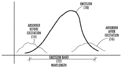
FIG. 1 is an illustrative graph of the response of the
emitter and absorber materials in accordance with the
present invention;
FIG. 2 is an illustrative graph of the response of the
emitter and absorber materials in accordance with an
alternate arrangement of the present invention;
FIGS. 3-5 depict various arrangements of layers
containing emitters and/or absorbers in accordance with
the present invention;
FIG. 6 depicts a security feature formed of ink;
FIG. 7 depicts security thread and fiber security
features;
FIG. 8 depicts planchette security features;
FIG. 9 depicts a cross-sectional view of a fiber
security feature; and
FIG. 10 depicts a graphic code security feature in
accordance with the present invention.
CA 02896803 2015-06-29
WO 2014/113042
PCT/US2013/026539
8
DETAILED DESCRIPTION OF THE INVENTION
The invention will be more completely understood
through the following detailed description, which should
be read in conjunction with the attached drawings. While
detailed embodiments of the invention are disclosed
herein, it is to be understood that the disclosed
embodiments are merely exemplary of the invention, which
may be embodied in various forms. Therefore, specific
functional details disclosed herein are not to be
interpreted as limiting, but merely as a basis for the
claims and as a representative basis for teaching one
skilled in the art to variously employ the invention in
virtually any appropriately detailed embodiment.
Most generally, the present invention provides
embodiments of systems and methods for document and
product authentication using optically encoded markings,
formed from at least one emitter and at least one
absorber, that exhibit a first emission in response to a
first excitation of the emitter and a change in that
emission in response to excitation of the absorber, such
that various combinations of emitter and absorber
materials create a machine readable response that cannot
be detected by the human eye. The encoded markings are
provided in the form of visible or invisible coatings
that exhibit one or more excited emissive and/or
absorptive responses that exhibit cumulative changes in
emissive response that are machine detectible.
The disclosed authentication system is intended
for authentication of products that include a substrate
that has been coated or embedded with the materials of
the present invention, including secure documents such
as banknotes, ID documents, Visas, and tax stamps. The
technology can also be used to authenticate a variety of
CA 02896803 2015-06-29
WO 2014/113042
PCT/US2013/026539
9
different consumer products and consumable goods that
are used in connection with appliances and the like.
Alternately, the security feature may be constructed as
a planchette, security thread or a planchette for
addition to substrates such as for example, paper.
As can best be seen at Fig. 1, the present
invention includes a security feature for authenticating
an article comprising, at least one emitter material
that generates an emission 10 within an emission band 12
in response to a first excitation and least one absorber
material that undergoes a change from a first absorption
characteristic 14 to a second absorption characteristic
16 within at least a portion of the emission band 12 of
the emitter material in response to a second excitation.
As a result, the change in the absorption
characteristics causes a non-apparent change in the
emission. In other
words, in response to a first
stimulation, the emitter material generates an emission,
as a second stimulation is applied, the absorber
undergoes a change that shifts its absorption
characteristics relative to the emission band resulting
in a nonvisible change in the emission band. This
nonvisible change representing a 5% or less shift in the
emission level however is machine detectible to allow a
detector to verify the authenticity of the security
feature. This is particularly advantageous as compared
to the prior art in that the resultant response is a
change in emission and not simply absorption thus
eliminating the need for the probes to locate whether a
change is in fact occurring.
It is preferred that the at least one emitter
within the present invention is selected from the group
consisting of: fluorescent materials, phosphorescent
CA 02896803 2015-06-29
WO 2014/113042
PCT/US2013/026539
materials, up-conversion materials and combinations
thereof. In this regard, the first excitation would be
an excitation consisting of the application of energy of
the type, wavelength and amplitude sufficient to cause
said emitter material to generate an emission.
Similarly, the at least one emitter may include more
than one emitters as depicted at Fig. 2 wherein a first
fluorescent emitter 10a and an up conversion emitter 10b
create respective emission responses when ultraviolet
energy and a 980nm pump diode are applied. These
emitters create emissions in their respective emission
bands 12a and 12b. As can
be seen the absorber
undergoes a change from a non-excited state 14 to an
excited state 16 relative to the emission bands 12a and
12b of the emitters 10a and 10b resulting in a
nonvisible emission change.
One skilled in the art should appreciate that the
machine readable change being detected may be a
detection of the emission across the entire emission
band in its aggregate or at one or more narrower
preselected points of the emission band.
It is further preferred that the at least one
absorber is selected from the group consisting of:
photochromic materials, thermochromic
materials,
electrochromic materials, magnetochromic materials,
mechanochromic materials and combinations thereof.
Excitation of the above materials is achieved by
applying energy of the appropriate type so as to induce
the change in the absorber material. It is within the
scope of the present invention that the first
stimulation energy appropriate to create an emission is
different in type and/or amplitude from the second
stimulation energy appropriate to induce a change in the
CA 02896803 2015-06-29
WO 2014/113042
PCT/US2013/026539
11
absorber. Further,
however, it is possible that the
first and second stimulation energies are of the same
type and vary instead only in amplitude. It should also
be appreciated by one skilled in the art that while the
figures herein depict an absorber that serves to
decrease the emission after the change is induced, there
are some materials in the absorber category that will in
fact undergo a change that results in a reduction in
their absorption characteristics when energized. As a
result, such materials would then cause a nonvisible
change in the form of an increase in the emission level.
In one embodiment as depicted at Fig. 3, the
security feature is formed as a coating 18 on a
substrate 20. The coating 18 is formed to include both
the emitter material 22 and the absorber material 24 in
a single coating.
Alternately, as depicted at Fig. 4,
the security feature is applied in two overlying
coatings, a first coating 18a containing the emitter
material 22 overlying the substrate 20 and a second
coating 18b containing the absorber material 24 applied
over the first coating 18a. Still
further, at Fig. 5,
should a substrate 20a have sufficient reflectivity,
then the coating 18b containing the absorber material 24
can be positioned adjacent the substrate 20a with the
coating 18b containing the emitter material 22
positioned thereon.
It is further within the scope of the present
invention to provide a coating wherein one or more
emitter materials are combined with one or more absorber
materials form a change that creates a covert, machine
detectible signature when appropriately excited using
the right combination and level of energy stimuli.
CA 02896803 2015-06-29
WO 2014/113042
PCT/US2013/026539
12
In one embodiment, the authentication process
includes detecting a time required for the absorber
material to relax to its original state after the
application if excitation energy is terminated. Since
the relaxation time for these materials is dependent on
both the material as well as the carrier in which the
material is embedded, timing of relaxation provides for
authentication of the carrier and relative composition
compounding percentages as well.
In one illustrative embodiment of the present
invention at Fig. 6, a substrate 20 is coated with the
emitter and absorber materials described above in the
form of an ink or dye 26. The ink
or dye 26 coating
contains an emitter material that is embedded with one
or more absorber materials. Further, the ink or dye 26
may be used to form indicia. When
first excitation
energy is applied the ink or dye 26 creates an emission
and at a second excitation the absorber causes a change
in the overall emission to yield verification as to the
presence or lack of the authentic coating.
At Fig. 7 the security feature can be seen as a
security thread 28 or fibers 30 within the substrate 20.
In the case of the fibers 30 or security threads 28, the
entire cross section may be a composition containing
both the emitter and absorber. Alternately, as seen in
Fig. 9, the fiber 30 may have a core 34 and a sheath 36
such that the core 34 contains preferably the emitter
material 22 and the sheath 36 contains preferably the
absorber materials 24.
In Fig. 8 it can be seen that a substrate 20 may
have planchettes 32 therein such that the planchettes 32
are formed to respond in accordance with the present
invention. In the case of planchettes 32 the planchette
CA 02896803 2015-06-29
WO 2014/113042
PCT/US2013/026539
13
is coated as described above relating to coated
substrates or formed to include the emitter and absorber
materials integrally therein.
In yet another embodiment, as seen at Fig. 10, the
present invention may be in the form of a graphic
feature or code that is created using alternating bands
of a coating 38 containing the emitter material 22 and a
coating 40 containing both the emitter 22 and absorber
24 materials. When excitation energy is applied the
entire surface and alternating bands appear to be a
single solid, uninterrupted feature. However as can be
seen below, the actual emission of the coating bands
results in high and low emission levels as detected
along the length of the substrate. While this coating
visually appears to be monolithic, when scanned using a
machine an encoded barcode appears that is actually made
up of slightly brighter and darker lines in a pattern
not visible to the eye.
While the invention has been described with
reference to illustrative embodiments, it will be
understood by those skilled in the art that various
other changes, omissions and/or additions may be made
and substantial equivalents may be substituted for
elements thereof without departing from the spirit and
scope of the invention. In addition, many modifications
may be made to adapt a particular situation or material
to the teachings of the invention without departing from
the scope thereof. Therefore, it is intended that the
invention not be limited to the particular embodiment
disclosed for carrying out this invention, but that the
invention will include all embodiments falling within
the scope of the appended claims. Moreover, unless
specifically stated any use of the terms first, second,
CA 02896803 2015-06-29
WO 2014/113042
PCT/US2013/026539
14
etc. do not denote any order or importance, but rather
the terms first, second, etc. are used to distinguish
one element from another.