Note: Descriptions are shown in the official language in which they were submitted.
CA 02897082 2015-07-02
WO 2014/109961 PCT/US2014/010185
Semiconductor Device Having Features to Prevent Reverse Engineering
This application claims priority to U.S. Patent Application No. 13/739,401,
filed January 11,
2013, which is a continuation-in-part of U.S. Patent Application No.
13/663,921, filed on
Oct. 30, 2012, which is a divisional of U.S. Patent Application No. 13/194,452
filed on July
29, 2011, which claims the benefit of U.S. Provisional Application Serial No.
61/494,172
filed June 7, 2011, which is incorporated by reference herein in its entirety.
BACKGROUND
It is desirable to design an electronic chip that is difficult to reverse
engineer to protect the
circuit design. Known reverse engineering techniques include methods for
tearing down
layers of the chip to expose the logic devices.
Semiconductor teardown techniques typically involve imaging a device layer,
removing the
layer, imaging the next layer, removing the layer, and so on until a complete
representation
of the semiconductor device is realized. Layer imaging is usually accomplished
using an
optical or electron microscope. Layer removal can be done by using physical
means such as
lapping or polishing, by chemical means by etching specific compounds, by
using a laser or
a focused ion beam technique (FIB), or by any other known method capable of
removing the
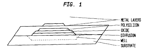
layers. Figure 1 shows some of the semiconductor layers and regions that are
imaged by the
teardown reverse engineering technique.
Once the semiconductor device teardown is complete and the imaging information
is
gathered, the logic function of the device can be re-constructed by using
diffusion,
polysilicon, and well areas to define the MOS devices used to create logic
gates, and the
metal layers to define how the logic gates are interconnected. Figure 2 shows
how the
semiconductor layers define the MOS device.
U.S. Patent No. 7,711,964 discloses one method of protecting logic
configuration data. The
configuration data for the logic device is encrypted and a decryption key is
encrypted using a
silicon key. The encrypted decryption key and configuration are transferred to
the logic
device. The silicon key is used to decrypt the decryption key which is then
used to decrypt
the configuration data. One problem with this method is that the chip is not
protected
against physical reverse engineering as described above.
1
CA 02897082 2015-07-02
WO 2014/109961 PCT/US2014/010185
Many other cryptography techniques are known. But, all cryptographic
techniques are
vulnerable to the conventional teardown techniques.
Disclosed is a method for designing a semiconductor device that is resistant
to these
techniques. The semiconductor device includes a physical geometry which is not
clearly
indicative of the device's function. For example, the semiconductor device is
designed
where two or more types of logic devices have the same physical geometry. When
the
teardown method is performed two or more devices will show the same physical
geometry,
but, these two or more devices have different logic functions. This prevents
the person
performing the reverse engineering to determine the logic functions by the
known methods
of observing the geometry of the devices.
Employing the disclosed method and device will force the reverse engineer to
employ more
difficult techniques. These techniques are more time consuming, more
expensive, and more
likely to have errors.
SUMMARY
The present method and device presents a semiconductor device that it is
difficult to reverse
engineer using known techniques.
In one aspect, a ROM circuit includes a first N channel transistor having an
output and
having device geometry and device characteristics adapted to bias the output
at a
predetermined level when a P channel circuit is connected to the first N
channel transistor; a
pass transistor connected between the output and a data bus, the pass
transistor connected to
a word line, the word line adapted to turn ON the pass transistor when the
word line is
asserted; and the P channel circuit connected to the data bus and adapted to
provide leakage
current to charge a gate in the first N channel transistor when pass
transistor is turned ON.
One device is an electronic element including a first device and a second
device. The first
device has a first geometry and a first characteristic and the second device
has a second
geometry and a second characteristic. The first geometry and the second
geometry are the
same and the second characteristic is different than the first characteristic.
The electronic
element may include additional devices. The devices may be active devices or
they may be
a silicided poly resistor and a non-silicided poly resistor.
A second device is an electronic circuit including a first logic device and a
second logic
device. At least one of the first logic device and the second logic device is
comprised of a
2
CA 02897082 2015-07-02
WO 2014/109961 PCT/US2014/010185
first device having a first geometry and a first characteristic, and a second
device having a
second geometry and a second characteristic. The first geometry and the second
geometry
are the same and the second characteristic is different than the first
characteristic.
A method of manufacturing a semiconductor device that is resistant to reverse
engineering is
provided. The method includes providing one or more invisible bias generators
having a
first device having a first geometry and a first characteristic, and a second
device having a
second geometry and a second characteristic, wherein the first geometry and
the second
geometry are the same and the second characteristic is different than the
first characteristic.
Multiple logic devices are provided and one or more invisible bias generators
are randomly
distributed within the logic devices.
A method of designing a semiconductor device that is resistant to reverse
engineering is
provided. The method includes providing one or more invisible bias generators
having a
first device having a first geometry and a first bias voltage, and a second
device having a
second geometry and a second bias voltage, wherein the first geometry and the
second
geometry are the same and the second bias voltage is different than the first
bias voltage.
The method also includes providing multiple logic devices; and randomly
distributing within
the logic devices the one or more invisible bias generator.
Another method of manufacturing a semiconductor device that is resistant to
reverse
engineering is provided. The method includes providing a substrate, providing
a first metal
layer, wherein outputs for electronic devices are located on the first metal
layer. The method
also includes providing a second metal layer, wherein gates for the electronic
devices are
located on the second metal layer, wherein the first metal layer is located
below the second
metal layer and it is necessary to remove the second metal layer in order to
test the level of
the outputs.
These and other features and objects of the invention will be more fully
understood from the
following detailed description of the embodiments, which should be read in
light of the
accompanying drawings.
In this regard, before explaining at least one embodiment of the invention in
detail, it is to be
understood that the invention is not limited in its application to the details
of construction
and to the arrangements of the components set forth in the description or
illustrated in the
drawings. The invention is capable of other embodiments and of being practiced
and carried
out in various ways. Also, it is to be understood that the phraseology and
terminology
3
CA 02897082 2015-07-02
WO 2014/109961 PCT/US2014/010185
employed herein, as well as the abstract, are for the purpose of description
and should not be
regarded as limiting.
As such, those skilled in the art will appreciate that the conception upon
which this
disclosure is based may readily be used as a basis for designing other
structures, methods,
and systems for carrying out the several purposes of the present invention. It
is important,
therefore, that the claims be regarded as including such equivalent
constructions insofar as
they do not depart from the spirit and scope of the present invention.
BRIEF DESCRIPTION OF THE DRAWINGS
The accompanying drawings, which are incorporated in and form a part of the
specification,
illustrate embodiments of the present invention and, together with the
description, serve to
explain the principles of the invention;
FIG. 1 illustrates semiconductor layers and regions that are imaged by the
teardown reverse
engineering technique;
FIG. 2 illustrates how the semiconductor layers define the MOS device;
FIG. 3 illustrates a circuit that is resistive to conventional reverse
engineering techniques;
FIG. 4 illustrates a circuit configuration using a level shifter;
FIG. 5 illustrates a second configuration using a level shifter;
FIG. 6 illustrates a circuit configuration without a comparator;
FIG. 7 illustrates a second circuit configuration without a comparator;
FIG. 8 illustrates an circuit configuration having six active devices;
FIG. 9A illustrates a multiplexer using the disclosed techniques;
FIG. 9B illustrates a second embodiment of a multiplexer using the disclosed
techniques;
FIG. 10 illustrates the implementation of a "NAND" logic function;
FIG. 11 illustrates the implementation of a "NOR" logic function;
FIG. 12 illustrates the implementation of a "INVERT" logic function;
FIG. 13 illustrates the implementation of a "BUFFER" logic function;
4
CA 02897082 2015-07-02
WO 2014/109961
PCT/US2014/010185
FIG. 14 illustrates the implementation of a "XOR" logic function;
FIG. 15 illustrates the implementation of a "XNOR" logic function;
FIG. 16A illustrates an IBG device having active components;
FIG. 16B illustrates alternative embodiments of IBG devices having active
components;
FIG. 17 illustrates a circuit comprised of resistors;
FIG. 18 illustrates a side view of a silicon wafer having active devices;
FIG. 19 illustrates another embodiment of a silicon wafer that is resistant to
electronic
testing of the chip;
FIG. 20A illustrates a cross section of a MOS semiconductor device;
FIG. 20B illustrates parasitic capacitances and resistances in semiconductor
device;
FIG. 21 illustrates an IBG circuit that utilizes parasitic capacitances.
DETAILED DESCRIPTION OF THE DRAWINGS
Many semiconductor processes that contain logic functions provide different
types of metal-
oxide-semiconductor (MOS) devices to be used in different environments. For
example, one
device can operate only at lower voltages and can be sized to minimum
geometry. Another
device can operate at higher voltages and cannot be sized to minimum geometry.
Using this
type of device allows the semiconductor device to interface to external
signals that are
higher in voltage when compared to the internal minimum sized devices.
The type of MOS device in the previous example is typically controlled by the
electrical
characteristics of the diffusion material. These characteristics are changed
by slightly
altering the atomic structure of this material by using an ion implant dose
and energy. This
process is normally described as "doping". This slight change of electrical
properties cannot
be detected by the conventional reverse engineering teardown techniques.
In order to provide a device that is resistant to these reverse engineering
techniques, an
invisible bias generator (IBG) has been developed. An IBG may be defined as an
electronic
device having at least two internal devices where the physical geometries of
the internal
devices cannot be used to determine the operating characteristics of the IBG.
5
CA 02897082 2015-07-02
WO 2014/109961
PCT/US2014/010185
One example of an IBG is a device where both internal devices have the same
geometry but
operate differently. For example, the first device may be a transistor that
operates at a first
voltage level and the second device is a transistor that operates at a
different voltage level.
In another example, the first device is a silicide resistor while the second
device is a non-
silicide resistor. In another example, conductive ink is used to create an
electronic circuit
and the amount of conductive material in the ink is changed between two of the
elements.
Another example of an IBG is a device where both internal devices have
different
geometries but have the same operating characteristics. For example, the first
device may be
a transistor that operates with first characteristics and the second device is
larger a transistor
that operates with the same characteristics. In another example, the first
device is a silicide
resistor while the second device is a non-silicide resistor. In another
example, conductive
ink is used to create an electronic circuit and the amount of conductive
material in the ink is
changed between two of the elements.
Another example of an IBG circuit includes devices having multiple possible
geometries and
multiple possible operating characteristics, with no apparent correlation
existing between a
given geometry and an operating characteristic.
FIG. 3 illustrates an exemplary IBG circuit 300 that provides an effective
deterrent to
semiconductor device teardown techniques. The circuit300 includes a first IBG
device
comprising a P-channel device301 and an N-channel device 303 which are
connected in
series between a power source (VCC) and a ground. A second IBG device
comprises a P-
channel device 302 and an N-channel device 304 also connected in series
between VCC and
ground. In one aspect of the present invention, the devices 301-304 may
comprise MOS
transistors. In a preferred embodiment, the devices 301-304 may also exhibit
identical
device geometry. The gates on the P-channel devices 301, 302 are floating as
they not
provided with an input signal (floating gates) and are charged via leakage
current to a
voltage level approximately VCC minus the threshold voltages of the devices
301 and 302,
each of the threshold voltages is independent. The gates on the N-channel
devices 303, 304
are also floating gates and are charged via leakage current to a voltage level
of
approximately ground plus the threshold voltages of the devices 303 and 304.
Each device 301-304 may include a conduction channel between a source and a
drain of the
device. The depth of the conduction channel is determined by the doping levels
of the
diffusion(also known as implantation) areas of the gates of devices 301-304
which in turn
6
CA 02897082 2015-07-02
WO 2014/109961 PCT/US2014/010185
determine the voltage level on the P and N channel device junctions, labeled
VA and VB in
FIG. 3.In one aspect of the present invention, the devices 301-304 are formed
with different
doping levels (also called impurity levels)between at least some of the
devices 301-304
while maintaining identical device geometry, thus resulting in the device
junctions VA and
VB having different voltage levels. A comparator 310 detects the voltage
levels of VA and
VB and based on the difference in these voltage bias levels outputs a
logical"1" or "0". VA
and VB can be any voltage level as the logic criteria of the comparator 310is
based on the
difference of these voltages. In a preferred embodiment, the circuit of FIG. 3
contains
identical geometry for the P and N channel devices 301-304, thus causing the
doping level
difference between the devices 301-304 to control the difference in the
voltage levels of the
device junctions VA and VB. For example, if devices 301 and 303 are doped to
form low
voltage MOS transistors (such as 2.5V, for example) and if devices 302 and 304
are doped
differently to form high voltage MOS transistors (such as 3.3V, for example),
then device
junction VA is at a higher voltage than device junction VB, and the output of
the comparator
will be a logical "1". As another example, if devices 301 and 304 are doped to
form low
voltage MOS transistors, and if devices 302 and 303 are doped to form high
voltage MOS
transistors, then device junction VA is at a lower voltage than device
junction VB, and the
output of the comparator will be a logical "0". The logic function of this
circuit is invisible
to reverse engineering teardown techniques since the operating voltages of the
device
junctions VA and VB are controlled by the doping levels and these doping
levels are not
determinable by conventional techniques.
For semiconductor technologies which provide different types of MOS devices,
such as the
high and low voltage devices described above, an advantage of the IBG circuit
is that it can
be easily constructed with current methods. Also, an IBG circuit in accordance
with one
aspect of the present invention can be used to create a number of different of
logic cells by
varying the number of high voltage devices and low voltage devices.
FIG. 4 shows an exemplary circuit 420 including an IBG and a level shifter
circuit which
produces a logical "1", or high, output in accordance with one aspect of the
present
invention. The IBG portion of the circuit 420 comprises transistors 401, 402,
405, and 406
each having a floating gate input.P-channel transistor 401 is connectedin
series with N-
channel transistor 405 at output node 401A, and P-channel transistor 402 is
connected in
series with N-channel transistor 406 at output node 402A. Each of the
transistors of the IBG
portion of the circuit can be a P-type or an N-type device. Also each
transistor can be a high
7
CA 02897082 2015-07-02
WO 2014/109961
PCT/US2014/010185
voltage device or a low voltage device. In a preferred embodiment, a high
voltage device
operates at 3.3 V while a low voltage device operates at 2.5 V. In an
exemplary
embodiment, transistor 402 is a low voltage P-type device,transistor 401 is a
high voltage P-
type device,transistor405is a low voltage N-type device, and transistor 406is
a high voltage
N-type device, resulting in the voltage level at output node 402A being higher
than the
voltage level at the output node 401A.For example, transistors 401 and 405 may
produce a
voltage level of about 100mV at the output node 401A and transistors 402 and
406 may
produce a voltage level of about 1.5 V at the output node 402A. These output
levels fall
short of being VCC and ground due to transistors 401, 402, 405, and 406 not
being fully
turned ON or OFF by the charge on their floating gates which are charged by
leakage
currents. Transistors 401, 402, 405 and 406 are selected to ensure the voltage
levels of the
output nodes 401A and 402A are such the one voltage level is higher and the
other voltage
level is lower than the threshold voltage of transistors 407 and 408,
described below.
The voltage levels of the output nodes 401A and 402A of the IBG circuit are
insufficient to
interface directly with digital logic due to the voltage level of the gates of
the transistors 401,
402, 405 and 406.To properly interface with digital logic, the signals from
the output nodes
401A and 402A are input to a level shifting circuit comprisingtransistors 403,
404, 407 and
408. Transistors 403 and 404 may comprise low voltage P-type devicesand
transistors 407
and 408 may comprise low voltage N-type devices. The output node 401A of the
IBG
circuitis connected to the gate of N-channel transistor 408 of the level
shifting circuit and the
output node 402A of the IBG circuit is connected to the gate of the N-channel
transistor 407
of the level shifting circuit.In an exemplary embodiment, the N-channel
transistors may have
a threshold voltage of about 700 mV. Thus, the 100 mV voltage level of node
401A which
is input to the gate of transistor 408 will turn transistor 408 "OFF" and the
1.5 V voltage
level which is input to the gate of transistor 407 will turn transistor 407
"ON". Thus,
transistor 403 will be turned "OFF" and transistor 404 will be turned "ON",
resulting in the
output of the level shifting circuit being a logical "1" or HI.
FIG. 4 also shows also an exemplary circuit 430 including an IBG and level
shifting circuit
which produces a logical "0", or low, output in accordance with one aspect of
the present
invention. The IBG portion of the circuit 420 comprises transistors 409, 410,
413, and 414
each having a floating gate input. P-channel transistor 409 is connected in
series with N-
channel transistor 413 at output node 409A, and P-channel transistor 410 is
connected in
series with N-channel transistor 414 at output node 410A. Each of the
transistors of the IBG
8
CA 02897082 2015-07-02
WO 2014/109961 PCT/US2014/010185
portion of the circuit can be a P-type or an N-type device. Also each
transistor can be a high
voltage device or a low voltage device. In a preferred embodiment, a high
voltage device
operates at 3.3 V while a low voltage device operates at 2.5 V. In an
exemplary
embodiment, transistor 409 is a low voltage P-type device, transistor 410 is a
high voltage P-
type device, transistor 413 is a high voltage N-type device, and transistor
414 is a low
voltage N-type device, resulting in the voltage level at output node 409A
being higher than
the voltage level at the output node 410A.For example, transistors 410 and 414
may produce
a voltage level of about 100 mV at the output node 410A and transistors 409
and 413 may
produce a voltage level of about 1.5 V at the output node 409A. Transistors
409, 410, 413
and 414 are selected to ensure the voltage levels of the output nodes 409A and
410A are
such the one voltage level is higher and the other voltage level is lower than
the threshold
voltage of transistors 415 and 416, described below.
The voltage levels of the output nodes 409A and 410A of the IBG circuit are
insufficient to
interface directly with digital logic due to the voltage level of the gates of
the transistors 409,
410, 413 and 414. To properly interface with digital logic, the signals from
the output nodes
409A and 410A are input to a level shifting circuit comprising transistors411,
412, 415 and
416. Transistors 411 and 412 may comprise low voltage P-type devices and
transistors 415
and 416 may comprise low voltage N-type devices. The output node 409A of the
IBG
circuit is connected to the gate of N-channel transistor 416 of the level
shifting circuit and
the output node 410A of the IBG circuit is connected to the gate of the N-
channel transistor
415 of the level shifting circuit. In an exemplary embodiment, the N-channel
transistors
may have a threshold voltage of about 700 mV. Thus, the 1.5 V voltage level of
node 409A
which is input to the gate of transistor 416 will turn transistor 416 "ON" and
the 100mV
voltage level which is input to the gate of transistor 415 will turn
transistor 415 "ON". Thus,
transistor 412 will be turned "OFF" and transistor 411 will be turned "ON",
resulting in the
output of the level shifting circuit being a logical "0" or LO.
As described above, the circuit420 gives the "HI" voltage output while
circuit430 gives the
"LO" voltage output. The geometry and size of the IBG transistors 401, 402,
405 and 406
of the circuit420may be identical to the geometry and size of the IBG
transistors 409, 410,
413 and 414 of thecircuit430. The only discernable difference between the two
devices is
the level of doping between the high voltage transistors and the low voltage
transistors.
Because the size and the geometry of IBG transistors of device 420may be
identical to the
9
CA 02897082 2015-07-02
WO 2014/109961
PCT/US2014/010185
IBG transistors of device 430, it is not possible to determine the difference
between these
two devices using the conventional reverse engineering teardown techniques.
FIG. 5 illustrates a second example of IBG circuits and level shifting
circuits to output a
"HI" or "LO" output. Similar to the embodiment shown in FIG. 4, there are 16
transistor
devices (501 through 516). Each of the transistors can be a P-type or an N-
type device.
Also each device can be a high voltage device or a low voltage device. In a
preferred
embodiment, a high voltage device operates at 3.3 V while a low voltage device
operates at
2.5 V. In an exemplary embodiment, transistors 502, 503, 504, 509, 511, and
512 are low
voltage P-type devices. Transistor 501 and 510 are high voltage P-type
devices. Transistors
505, 507, 508, 514, 515, and 516 are low voltage N-type devices. Transistors
506 and 513
are high voltage N-type devices. Device 520 gives the "HI" voltage output
while device 530
gives the "LO" voltage output. The geometry and size of the IBG transistors
501, 502, 505,
and 506 of the device 520may be identical to the geometry and size of
transistors 509, 510,
513 and 514 of device 530. The only discernable difference between the two
devices is the
level of doping between the high voltage transistors and the low voltage
transistors. Because
the size and the geometry ofthe IBG transistors ofdevice 520 is identical to
that of the IBG
transistors of device 530 it is not possible to determine the difference
between these two
devices using the conventional reverse engineering teardown techniques.
If a semiconductor chip contains an IBG as described in FIG. 4 or FIG. 5, it
is extremely
difficult for someone trying to reverse engineer the chip using teardown
techniques to
determine the function of the IBG devices placed on the chip because the
geometry of the
internal devices are the same.
FIG. 6 and FIG. 7 illustrate examples of IBGs where the voltage levels of the
outputs of the
circuits are sufficient to directly interface with the devices on a chip. In
FIG. 6, device 601
is a high voltage P-type device, such as 3.3v, device 602 is a low voltage P-
type device, such
as 2.5v, device 603 is a low voltage N-type device and 604 is a high voltage N-
type device.
By connecting the gate of device 601 to the gate of device 602, these devices
share the
leakage current, resulting in the high voltage device 601 being fully turned
OFF and the low
voltage device 602 being fully turned ON. Similarly, by connecting the gate of
device 603
to the gate of device 604, these devices share the leakage current, resulting
in the low
voltage device 603 being fully turned ON anddevice 604 being fully turned OFF.
Output
node 601A will be sufficiently close to ground to function as a logical "0"
and interface
CA 02897082 2015-07-02
WO 2014/109961 PCT/US2014/010185
directly with other CMOS devices and output node 602A will be sufficiently
close to VCC
to function as a logical "1" and interface directly with other CMOS devices.
In FIG. 7, device 701 is a low voltage P-type device, such as 2.5 V, device
702 is a high
voltage P-type device, such as 2.5 V, device 704 is a low voltage N-type
device and 703 is a
high voltage N-type device. By connecting the gate of device 701 to the gate
of device 702,
these devices share the leakage current, resulting in the low voltage device
701 being fully
turned ON and the high voltage device 702 being fully turned OFF. Similarly,
by
connecting the gate of device 703 to the gate of device 704, these devices
share the leakage
current, resulting in the high voltage device 703 being fully turned OFF and
low voltage
device 704 being fully turned ON. Output node 701A will be sufficiently close
to VCC to
function as a logical "1" and interface directly with other CMOS devices and
output node
702A will be sufficiently close to ground to function as a logical "0" and
interface directly
with other CMOS devices.
The geometry and size of the IBG transistors 601, 602, 603 and 604 may be
identical to the
geometry and size of the IBG transistors 701, 702, 703 and 704 The geometry
and size of
IBG transistors 601, 602, 603, and 604 may not be identical to each other. The
geometry
and size of IBG transistors 701, 702, 703 and 704 may not be identical to each
other.
Additionally, the voltage levels at the gates of the gate connected
transistors are equal. The
only discernible difference between the two devices is the level of doping
between the high
voltage transistors and the low voltage transistors. Because the size and the
geometry of
IBG transistors of Fig. 6 may be identical to the IBG transistors of device
Fig. 7, it is not
possible to determine the difference between these two devices using the
conventional
reverse engineering teardown techniques. The IBG shown in FIG. 6 has the same
geometry
as the IBG shown in FIG. 7 with the only difference being the doping level of
some of the
transistors. Therefore, if a chip is designed using the IBG illustrated in
FIG. 6 and the IBG
illustrated in FIG. 7, it is very difficult to determine a difference in the
function of the
devices made by each design.
The IBG shown in FIG. 6 can include different configurations. In one example,
device 601 is
a low voltage P-type device, device 602 is a high voltage P-type device,
device 603 is a low
voltage N-type device and 604 is a high voltage N-type device. In another
example device
601 is a high voltage P-type device, device 602 is a low voltage P-type
device, device 603 is
a high voltage N-type device and 604 is a high voltage N-type device. In
another example
11
CA 02897082 2015-07-02
WO 2014/109961 PCT/US2014/010185
device 601 is a high voltage P-type device, device 602 is a low voltage P-type
device, device
603 is a low voltage N-type device and 604 is a low voltage N-type device. In
another
example device 601 is a high voltage P-type device, device 602 is a low
voltage P-type
device, device 603 is a low voltage N-type device and 604 is a high voltage N-
type device.
There are a total of sixteen configurations possible for a four device IBG.
FIG. 8 illustrates another embodiment of an IBG circuit. Devices 801, 802, 803
are shown
as P-type devices and can be any combination of high voltage or low voltage
devices.
Devices 804, 805, 806 are shown as N-type devices and can be any combination
of high
voltage or low voltage devices. However, the six devices shown can be any
combination of
P-type and N-type devices. The six device IBG has a total of 64 possible
configurations.
Furthermore, an IBG can be comprised of any number of active devices with 2 to
the "n"
number of combinations, where n is the number of active devices.
FIG. 9A and FIG. 9B illustrate IBG circuits which include multiplexers.
Because IBG
circuits may be used to select logic functions, it is convenient to implement
these circuits in
conjunction with digital multiplexers that effectively steer one of two inputs
to its output.
These IBG based multiplexers select an input base solely on the IBG function.
In Fig. 9A,
transistors 901, 902, 905 and 906 comprise an IBG circuit and transistors 903,
904, 907 and
908 comprise a multiplexer. In Fig. 9B, transistors 911, 912, 915 and 916
comprise an IBG
circuit and transistors 917, 918, 913 and 914 comprise a multiplexer. In FIG.
9A, devices
901 and 906 are 3.3V devices while devices 902, 903, 904, 905, 907, and 908
are 2.5V
devices. Inverter 910 provides the inverse of input A and the inverse of input
B. In FIG. 9B,
devices 912 and 915 are 3.3V devices while devices 911, 913, 914, 916, 917,
and 918 are
2.5V devices. Inverter 920 provides the inverse of input A and the inverse of
input B.
Based on the outputs of the IBG transistors 901, 902, 905 and 906, the
multiplexer shown in
FIG. 9A selects the B input while the multiplexer shown in FIG.9B selects the
A input based
on the outputs of the IBG transistors 911, 912, 915 and 916. The only
discernible difference
between the two devices is the level of doping between the high voltage
transistors and the
low voltage transistors. Because the size and the geometry oftransistors of
Fig. 9A may be
identical to the transistors of Fig. 9B, it is not possible to determine the
difference between
these two devices using the conventional reverse engineering teardown
techniques. The IBG
shown in FIG. 9A may have the same geometry as the IBG shown in FIG. 9B with
the only
difference being the doping level of some of the transistors. Therefore, if a
chip is designed
using the circuit illustrated in FIG. 9A and the circuit illustrated in FIG.
9B, it is very
12
CA 02897082 2015-07-02
WO 2014/109961 PCT/US2014/010185
difficult to determine a difference in the function of the devices made by
each design.The
only difference between these circuits is the configuration of 3.3V and 2.5V
devices.
FIG. 10 represents the implementation of a "NAND" logic function and FIG. 11
illustrates
the implementation of a "NOR" logic function. In FIG. 10, NAND gate 1010 and
NORgate1011 output to an IBG based multiplexer1012, such as the IBGcircuit
multiplexer
shown in Fig. 9A, which selects the output of the NAND gate 1010. In FIG. 11,
NANDgate1110 and NORgate1111 output to an IBG based multiplexer1112, such as
the
IBG circuit multiplexer shown in Fig. 9B, which selects the output of the NOR
gate 1111.
These two implementations appear to identical during reverse engineering
because the
difference between these configurations is the IBG circuit. Without knowledge
of the IBG
circuit the logic function of these configurations is indeterminate.
FIG. 12 illustrates an implementation of the logic function "INVERT"
comprising an
inverter 1201 and an IBG based multiplexer 1202, such as the IBG circuit
multiplexer shown
in Fig. 9A, implemented to select the inverted input. FIG. 13 illustrates an
implementation
of the logic function "BUFFER" comprising an inverter 1301 and an IBG based
multiplexer
1302, such as the IBG circuit multiplexer shown in Fig. 9B, implemented to
select the non-
inverted input.FIG. 14 illustrates an implementation of the logic function
"XOR" comprising
an exclusive-or gate 1401, an inverter 1403 and an IBG based multiplexer 1402,
such as the
IBG circuit multiplexer shown in Fig. 9A, implemented to select the output of
the gate 1401.
FIG. 15 illustrates an implementation of the logic function "XNOR" comprising
an
exclusive-nor gate 1501, an inverter 1503 and an IBG based multiplexer 1502,
such as the
IBG circuit multiplexer shown in Fig. 9B, implemented to select the output of
the inverter
1503. As with the previous examples, reverse engineering a chip that has both
the
"INVERT" of FIG. 12 and the "BUFFER" of FIG. 13 will be difficult to perform
because
the "INVERT" and the "BUFFER" will have the same appearance. Reverse
engineering a
chip that has both the "XOR" of FIG. 14 and the "XNOR" of FIG. 15 is difficult
because the
"XOR" and "XNOR" have the same appearance. As described above, each pair of
implementations is indeterminate without knowledge of the logical operation of
the IBG
circuit based multiplexers.
One advantage of the high voltage / low voltage method of anti-reverse
engineering deterrent
is that most processes support this distinction. Many implementations are
designed to use
low voltages internal voltages because as feature size decreases the internal
voltage
13
CA 02897082 2015-07-02
WO 2014/109961 PCT/US2014/010185
decreases. But, many devices outside of the chip operate at higher voltages
and the chips
must be able to interface with these devices. Therefore, devices that use
higher voltages are
still used and being developed. It is possible to for the difference between
the low voltage
device and the high voltage device to be achieved using small doping changes
between P and
N devices.
The IBG devices described above include active devices that use the dopant
level to control
characteristics of the devices. As an example, it is known in a particular
process that a
doping concentration difference between the 2.5V and 3.3V devices is about
8xE16
atoms/cm3. Structures that have doping density differences below 1xE17 are
candidates for
IBG design. Examples of IBGs are in FIG. 16.
There are many other combinations of devices that will work besides the 2.5V
and 3.3V
devices. For example, a 2.5V can be used with a 5V device. A 1.8V device, a
1.5V device,
or a 1.2V can be used with a 3.3V device. A 1.2V device can be used with 1.8V
or a 2.5V
device. A 1.0V device can be used with a 1.8V device, 2.5V device, or a 3.3V
device. A
0.85V device can be used with a 1.8V device, a 2.5V device, or a 3.3V device.
This list is
exemplary only and any combination of devices that can be made with the same
physical
geometry can be used.
The previous examples illustrate some of the possible implementations of IBG
devices using
active devices. Another way to achieve an IBG device is to use inactive
devices. The IBG
can be made using a silicide poly resistor and a non-silicide poly resistor.
The first device is
used to set the first bias voltage as an active bias voltage and the second
device is used to set
the set the second bias voltage as an active bias voltage. The difference
between the silicide
poly resistor and the non-silicide poly resistor will not be apparent to the
conventional
reverse engineering techniques because the resistors have the same geometry.
FIG. 16A
illustrates an example of an IBG device. FIG. 16B illustrates other examples
of an IBG
device.
Polysiliconhas fairly high resistivity, about a few hundred S1-cm. Resistive
devices from
polysilicon suffer from this high resistivity because as the device dimension
shrinks the
resistance of the polysilicon local interconnection increases. This increased
resistance
causes an increase in the power consumption and a longer RC time
delay.Silicides are added
to polysilicon devices because the addition of the silicides reduces the
resistance and
increases device speed. Any silicide that has a much lower resistivity than
polysilicon may
14
CA 02897082 2015-07-02
WO 2014/109961 PCT/US2014/010185
be used. Titanium silicide (TiSi2) and tungsten silicide (WSi2) are two
silicides that are
commonly used.
Next, one method of forming a silicide device is described. A self-aligned
silicide process is
conventionally used to from Titanium Silicide. Initially, chemical solutions
are used to clean
the wafer surface in order to remove contaminants and particles. Next, the
wafer is sputtered
in a vacuum chamber using argon to remove the native oxide from the wafer
surface. Next,
a layer of the wafer surface is sputtered to deposit a layer of titanium on
the wafer surface.
This results in a wafer having the silicon exposed at the source/drain and on
top of the
polysilicon gate. Next, a titanium silicide is formed on the polysilicon by
using a thermal
annealing process. For example, annealing can be performed in a rapid thermal
process to
form titanium silicide on top of the polysilicon and on the surface of the
source/drain.
Because titanium does not react with silicon dioxide, silicide is formed only
where
polysilicon directly contacts with titanium. Next, the unreacted titanium is
removed by
using a wet etch process that exposes the unreacted titanium to a mixture of
hydrogen
peroxide (H202) and sulfuric acid (H2504). Lastly, the wafer is annealed which
increases
the grain size of the titanium Silicide. The increased grain size improves the
wafer's
conductivity and reduces wafer's contact resistance.
Another characteristic that can be controlled in the IBG device is the
threshold voltage. The
threshold of MOS transistors can be controlled by threshold adjustment
implant. An ion
implantation process is used to ensure that the power supply voltage of the
electronic
systems can turn the MOS transistor in the IC chip on and off The threshold
adjustment
implantation is a low-energy and low current implantation process. Typically,
the threshold
adjustment implantation is performed before gate oxide growth. For CMOS IC
chips, two
threshold adjustment implantation processes are needed, one for p-type and one
for n-type.
In an IBG device, the process described above can be used to produce resistors
that have the
same physical dimensions and have different resistance. Conversely, the
process can be
used to produce resistors that have different geometries and the same
resistance.
FIG. 17 illustrates an example of an IBG device implemented by silicide
resistors. A voltage
source VCC is connected to a circuit having resistors 1701, 1702, 1703, 1704.
The
resistance of the resistors can be set by the method described above to have
two different
resistance levels with all of the resistors having the same physical geometry.
For example,
resistors 1701 and 1704 may be non-silicide resistors while resistors 1702 and
1703 are
CA 02897082 2015-07-02
WO 2014/109961 PCT/US2014/010185
silicide resistors. In this example if Va is less than Vb then the output of
the device is a logic
"1." If Va is greater than or equal to Vb then the output of the device is a
logic "O."
In another embodiment, the devices can be formed using conductive inks.
Conductive inks
are used to print circuits on a variety of substrate materials. Conductive
inks contain
conductive materials such as powdered or flaked silver materials.
Conductive inks can be used to implement IBG circuits because the properties
of the inks
used to print the circuit can be varied to create devices that have different
properties. For
example, some devices can be printed using conductive ink having an amount of
conductive
material. Then, conductive ink that has more (or less) conductive material is
used to print
another portion of the circuit. The circuit then can have devices that look
similar and operate
differently or look different and operate the same.
One possible method of reverse engineering IBG circuits is to physically
measure the
devices in the circuit. This can be done using a probe to measure the actual
voltage
generated by the circuit. In order to thwart this method of reverse
engineering, the IBG cells
are placed randomly spaced throughout the design. This makes it more difficult
to probe the
large number of IBG circuits required to reverse engineer the design.
In an alternative embodiment, the types of IBG circuits used are randomly
distributed. For
example, every third "AND" gate is implemented using an IBG circuit while
every fourth
"NAND" gate is implemented using an IBG circuit. As the number of devices
implemented
by IBG circuits is increased, the difficulty in reverse engineering the chip
is increased.
Additionally, as the number of types of logic devices implemented by IBG is
increased, the
difficulty in reverse engineering the chip is increased.
In another embodiment, logic blocks are made having logic devices therein.
Within each
logic block, the IBGs are randomly distributed within the logic block. As a
result, different
types of logic devices within each logic block are comprised of IBG devices.
In another embodiment, logic blocks are made having logic devices. The
designer
determines for the logic blocks a critical point and uses an IBG to implement
the critical
point. The critical point is a point within the logic the block where it is
necessary to know
the function or output value in order to determine the function of the logic
block.
Implementing the critical point within the logic block by an IBG is
advantageous because
this ensures that IBG has maximum effect in preventing reverse engineering.
The inability
16
CA 02897082 2015-07-02
WO 2014/109961
PCT/US2014/010185
to determine the value of critical point will necessarily prevent the reverse
engineer from
determining the proper function for the logic block.
For example, if the logic block is an ADDER, replacing a digit in the output
can make it
impossible to determine the function of the adder. That is because someone
trying to reverse
engineer the chip monitoring the function of the logic block would expecta
specific output
for an ADDER. When the replaced digit does not give the expected result, it is
not
determined that the logic block is functioning as and ADDER.
Another advantage of the disclosed system and method is that chip can be
designed using
standard tools and techniques. Methods of designing a chip are described in
the following
paragraphs.
A designer creates an overall design for the chip and for logic blocks within
the chip. The
design is created in a known hardware design language such as Verilog or VHDL.
The
design is then synthesized into standard logic which converts the design to
the optimized
gate level. Synthesis may be performed using standard synthesis tools such as
Talus Design,
Encounter RTL Designer, and Design Compiler. The synthesis maps the logic
blocks into
standard logic using a standard cell library provided by the supplier. Next, a
place and route
tool is used to create a physical implementation of the design. This step
involves creating a
floorplan, a power grid, placing the standard cells, implementing a clock
tree, and routing
connectivity between cells and input/output pins. Some examples of place and
route tools
are Talus Vortex, Encounter Digital Implementation, and IC Compiler. Using
this process
there are various ways to design a chip using IBG devices. One way is to
create and
characterize one or more new standard cell libraries and use the one or more
new standard
cells at the beginning of the process. Another approach is to place the IBG
devices during
the place and route step, either automatically or manually.
Another method of designing a chip is for the designer to create the design
using a schematic
entry tool. The designer creates a circuit by hand comprising the base logic
gates. The
designer can optimize the logic functionality using Kamaugh-maps. A layout
entry tool is
used to create the physical implementation of the design. The designer draws
polygons to
represent actual layers that are implemented in silicon. Using this approach
the designer
places IBG devices at any desired location.
Because the above devices result in a design that is difficult to reverse
engineer using the
conventional tear down techniques, another method may be implemented to
reverse engineer
17
CA 02897082 2015-07-02
WO 2014/109961 PCT/US2014/010185
the chip. Another known method of reverse engineering is to probe the device
while active
in order to establish the operating values of the internal devices. In order
to perform these
methods, the reverse engineer must remove some layers of the wafer to expose
the output
contacts of the devices. One way to make this technique more difficult is to
randomly place
the logic devices as described above. Another technique is to design a chip
that is physically
resistant to these techniques.
FIG. 18 illustrates the layers of a silicon wafer that is resistant to
electronic testing of the
chip. The wafer has a base layer 1801 that includes the diffusion layer. The
oxide layer
1802 is on top of the diffusion layer 1801. The polysilicon layer 1803 is
located on top of
the oxide layer with the metal layer 1 1804 located thereon. The signal
outputs are formed
in metal layer 1 1804. Metal layer 2 1805 is located on top of the metal layer
1 1804. The
gate connections are formed in metal layer 2 1805. With this layout it is
necessary to
remove a portion of metal layer 2 1805 in order to probe the signal outputs
that are located in
metal layer 1 1804. Removing a portion of metal layer 2 1805 disrupts the gate
connections
of the devices which in turn deactivates the devices. Thus, a reverse engineer
trying to probe
the device will destroy the functionally of the device during the reverse
engineering process.
In many of the techniques described above, the output voltage level of a
device is used to
determine the operation of the device. But, any other operating characteristic
of the device
could be used. For example, the rise time of the device, the current drawn, or
the operating
temperature can be used in the IBG. Also, more than one physical property of
the device can
be varied. For example, the geometry and the doping level can be controlled to
implement
an IBG.
FIG. 19 illustrates another embodiment of a silicon wafer that is resistant to
electronic
testing of the chip. In this embodiment, a top metal layer 1901 is provided.
Multiple
floating gates are connected to the top metal layer 1901. The connection can
be a direct
connection, or the gates can be connected through several layers of metal to
the top metal
layer 1901. The top level metal layer 1901 may be applied without any
connection
(floating). Additionally, it may be desirable to maintain a gap between the
solid top level
metal layer 1901 and the top level metal of the floating gates in order to
minimize
capacitance for proper IBG operation. As with the embodiment illustrated in
FIG. 18,
removing a portion of metal layer 1901 disrupts the gate connections of the
devices which in
turn deactivates the devices. Thus, a reverse engineer trying to probe the
device will destroy
18
CA 02897082 2015-07-02
WO 2014/109961 PCT/US2014/010185
the functionally of the device during the reverse engineering process.
Furthermore, if the top
metal layer 1901 is exposed to energy from an ion beam source, the s
"floating" metal layer
attracts the charge emanating from the ion beam source. This accumulated
charge will cause
MOSFET gate breakdown and create shorts between the gate, source, and drain of
the
floating gate device. This increases the current draw of the floating gate
device and renders
the circuit inoperative. A single ion beam edit through the security shield
may initiate
MOSFET gate breakdown for several floating gate devices.
In many of the techniques described above, the output voltage level of a
device is used to
determine the operation of the device. But, any other operating characteristic
of the device
could be used. For example, the rise time of the device, the current drawn, or
the operating
temperature can be used in the IBG. Also, more than one physical property of
the device can
be varied. For example, the geometry and the doping level can be controlled to
implement
an IBG.
Another operating characteristic that is used the parasitic capacitances that
are formed within
MOSFET circuitry. FIG. 20A illustrates a cross section of a MOS semiconductor
device.
The semiconductor device has a top plane and a bottom plane with a top
dielectric layer, an
intra dielectric layer, a bottom dielectric therebetween. The top and intra
dielectric layers are
typically comprised of metal, while the bottom dielectric layer is typically a
substrate,
diffusion, polysilicon, or metal structures.
As shown in FIG. 20B, capacitors are formed in vertical and horizontal
dimensions
surrounding the structures because of the physical conductor-dielectric-
conductor
configuration of the MOS fabrication process. These capacitors are typically
very small in
value and considered parasitic for most designs. In addition, the metal
connections in a
circuit have resistance defined by the manufacturing process. Typically these
metal
resistances are low value and considered to be parasitic for most
applications.
Semiconductor devices that utilize floating gates are sensitive to these
parasitic capacitances.
Because an IBG device is based on floating gates, parasitic capacitances can
be utilized to
determine the state of the circuit. FIG. 21 illustrates an IBG device such as
the one
illustrated in FIG. 6 or FIG. 7. In FIG. 21, the resistors and capacitors
illustrate the parasitic
resistances and capacitances that are present in the circuit. Even if Ql, Q2,
Q3, and Q4 have
identical geometries and doping densities, the circuit output can be
determined by the
specific values of Cl thru C6, R1, and R2. In this case whether the IBG cell
produces a "1"
19
CA 02897082 2015-07-02
WO 2014/109961 PCT/US2014/010185
or a "0" is determined solely by the parasitic capacitance and resistance.
This makes reverse
engineering of the IBG circuit even more difficult. The reverse engineer has
to account for
small variations in doping levels and the parasitic capacitances and
resistances that are
present in order to determine the state of the IBG device.
Although the embodiment above describes parasitic capacitances and
resistances, floating
gate devices are sensitive to other parasitic elements. For example, a
parasitic inductance
may be used to change the operation of an IBG circuit.
The many features and advantages of the invention are apparent from the
detailed
specification. Thus, the appended claims are intended to cover all such
features and
advantages of the invention which fall within the true spirits and scope of
the invention.
Further, since numerous modifications and variations will readily occur to
those skilled in
the art, it is not desired to limit the invention to the exact construction
and operation
illustrated and described. Accordingly, all appropriate modifications and
equivalents may be
included within the scope of the invention.
Although this invention has been illustrated by reference to specific
embodiments, it will be
apparent to those skilled in the art that various changes and modifications
may be made
which clearly fall within the scope of the invention. The invention is
intended to be protected
broadly within the spirit and scope of the appended claims.