Note: Descriptions are shown in the official language in which they were submitted.
CA 02897160 2016-09-15
1
A SYSTEM FOR REGULATING THE OUTPUT OF A HIGH-VOLTAGE,
HIGH-POWER, DC SUPPLY
FIELD OF THE INVENTION
This invention relates to a system for regulating the output of a high-
voltage,
high-power, DC power supply.
BACKGROUND OF THE INVENTION
Conventional modulators used in pulsed accelerators produce electrical pulses
that drive radio frequency (RF) tubes. The RF output from these tubes produces
an
electric field in acceleration cavities and the electric field accelerates the
charged
particles. The acceleration cavities can either be normally-conducting or
superconducting. The pulses in normally-conducting cavities arc typically only
a few
microseconds long to minimize the resistive dissipation in the cavities. Since
there is
very little dissipation in superconducting cavities, the pulses for these are
much
longer, typically of order a few milliseconds, because this reduces the peak
power
required.
One example of a current long-pulse modulator is at the Spallation Neutron
Source (SNS) at Oak Ridge National Laboratory. The specification for this
modulator
CA 02897160 2015-07-03
WO 2014/113077
PCT/US2013/059145
2
is shown in Table 1 below:
Voltage 85 kV
Current 165 A
Pulse Width 1.5 ms
Repetition Rate 60 Hz
Voltage Flatness 1%
Table 1. SNS modulator specification.
Ideally, such a pulse modulator would provide very flat pulses (constant
voltage), at high efficiency and low cost, in a compact and reliable
configuration.
These factors present a number of challenges. One challenge associated with
long,
e.g., millisecond scale, pulses at high current is that they couple
substantial charge,
which decreases the voltage on the capacitors in the modulator. This voltage
decrease
is often referred to as droop. It is typically desirable to limit the
capacitor droop to a
few percent or less. While it is conceptually possible to increase the
capacitance to
limit this droop, the size of a capacitor needed to achieve this is typically
too large to
be practical. For example, limiting the capacitor droop to 1% in the SNS
modulator
discussed above would require a capacitor bank that stores about 1.1 M.1.
Instead, an
alternate means of reducing capacitor droop regulation is needed.
Another problem associated with pulsed modulators is that they do not draw
constant power. Pulse modulators typically draw power in a pulsed fashion,
which
transiently decreases the voltage on the AC lines, a phenomenon known as
flicker
(named because it makes electric lights flicker). Flicker can be highly
disruptive to
both local power users and the grid itself.
There are several conventional modulator designs which have been deployed
in large accelerator systems. Each of these has one or more drawbacks in its
implementation, as discussed below. One of the significant challenges to these
CA 02897160 2015-07-03
WO 2014/113077
PCT/US2013/059145
3
designs is the need to regulate voltage droop in a long-pulse modulator.
Historically, droop regulation has been done by dissipating power with a
vacuum tube. However, the power dissipated in a vacuum tube would be
substantial.
For example, a system with 10% droop would require at least 5% average
dissipation,
which would be 63 kW in each of the fifteen SNS modulators.
In high-power modulators, it is desirable to regulate droop without such
dissipation. There are several techniques currently used to regulate droop
without
dissipation. One is a power converter modulator, such as the one currently
implemented at the SNS. This power converter design includes a semiconductor
switch bridge circuit that produces pulses of alternate voltage. The pulses
are stepped
up by a transformer, then rectified to deliver the output pulse. To provide a
flat output
pulse as the voltage on the bus capacitor droops, the width of the alternating
pulses is
increased over time, similar to pulse-width modulation in a switching power
supply.
One problem with this implementation is the bridge circuit switches full power
repeatedly during a pulse. Such a design requires large switching transistors.
To
reduce the switching losses in the transistors, the bridge circuit may be
resonant.
However, this adds significant complexity to the device. Developing the
modulator
system for the SNS has taken ten years and has had multiple failures in the
switching
transistors, the resonant capacitors across the IGBTs, and the high-voltage
transformers. Moreover, the droop regulation is not yet functional.
Another conventional system used to regulate droop in a long-pulse modulator
is a bouncer modulator. The bouncer modulator compensates for the droop with
an
auxiliary capacitor and inductor. Both the main power supply and the bouncer
power
supply for the bouncer modulator need to be well-regulated to provide an
accurate
CA 02897160 2015-07-03
WO 2014/113077
PCT/US2013/059145
4
output voltage, and therefore need to be switching power supplies. A high-
power
main switching supply is significantly more expensive than an SCR-controlled
supply,
which cannot be used in this architecture.
Another conventional design is a pulse-step modulator, which operates with
multiple stages that are charged in parallel by a transformer then switched in
series.
The power flows through a boost regulator, which is controlled to provide a
constant
power draw which reduces flicker. One problem with the conventional pulse-step
modulator is that the boost regulators need to be large enough to carry all
the power.
This is much more expensive than an SCR-controlled power supply. The pulse
step
modulator is also large because of the high-voltage charging transformer.
Yet another conventional system used to regulate droop in a long-pulse
modulator is a Marx generator. The Marx generator is similar to the pulse-step
modulator because multiple stages are charged in parallel, then switched in
series.
The main difference is the Marx generator charge current passes up the chain
of
stages, while the pulse-step modulator charges through a transformer with
multiple
secondary windings. Additional Marx stages can be switched on during the pulse
to
compensate for droop, which add to the overall cost and complexity of the
modulator.
Such a design also requires an expensive switching power supply to eliminate
flicker.
Accelerators can also be designed to operate continuously rather than being
pulsed. While voltage regulation is important for these systems as well, the
major
concern is ripple on the output pulse rather than droop. An example of a
continuous
accelerator is the Advanced Photon Source (APS) at Argonne National
Laboratory.
The APS modulator parameters are shown in Table 2 below. The large amount of
ripple is because the high-voltage power supply is SCR-controlled. While a
switching
CA 02897160 2015-07-03
WO 2014/113077
PCT/US2013/059145
supply would produce much less ripple, it would be more expensive.
Voltage 100 kV
Current 20A
Present Ripple 1.3 kV p-p
Table 2. APS modulator parameters.
There are several conventional approaches to mitigate the ripple from the
power supply. In one example, a modulating-anode supply reduces the ripple
voltage
between the cathode and the modulating anode, and low-level RF feedback
compensates for the remaining ripple. Although this method is somewhat
effective, it
may be necessary in some instances to reduce the ripple even further.
Thus, there is a need for a system which regulates the output of a high-
voltage,
high-power, DC supply to reduce capacitor droop and DC ripple.
BRIEF SUMMARY OF THE INVENTION
The subject invention, however, in other embodiments. need not achieve all
these objectives and the claims hereof should not be limited to structures or
methods
capable of achieving these objectives.
In one aspect, a system for regulating the output of a high-voltage, high-
power
DC supply is featured. The system includes a high-voltage DC power supply, a
storage capacitor, and at least one non-dissipative regulator having an output
voltage
range less than an output voltage range of the high-voltage DC power supply.
The
regulator includes an internal storage and a control circuit configured to
maintain a
desired high-voltage output on a load.
In one embodiment, the storage capacitor and at least one non-dissipative
CA 02897160 2015-07-03
WO 2014/113077
PCT/US2013/059145
6
regulator may be connected in series. The high-voltage DC power supply may be
connected in parallel with the series combination of the storage capacitor and
the at
least one non-dissipative regulator. The high-voltage DC power supply
connected in
parallel with the series combination of the storage capacitor and the at least
one non-
dissipative regulator may include a modulator comprising at least one
switching
device. The high-voltage power supply and the storage capacitor may be
connected in
parallel. The at least one non-dissipative regulator may be connected in
series with
the parallel combination of storage capacitor and high voltage power supply.
The at
least one non-dissipative regulator connected in series with the parallel
combination
of storage capacitor and high voltage power supply may include a modulator
comprising at least one switching device. The at least one non-dissipative
regulator
may be connected in series with the high-voltage power supply. The series
combination of the power supply and at least one non-dissipative regulator may
be
connected in parallel with the capacitor. The series combination of the power
supply
and at least one non-dissipative regulator connected in parallel with the
capacitor may
include a modulator comprising at least one switching device. The system may
include a modulator including at least one switching device. The regulator may
be
configured to cancel variations in the high-voltage output to provide a flat
high-
voltage. The control circuit may be configured to maintain the desired high-
voltage
on the load by measuring load voltage and adjusting the regulator voltage such
that the
sum of the regulator voltage and the storage capacitor voltage equals the
desired high-
voltage. The at least one regulator may include a plurality of regulators
connected to
provide a greater voltage adjustment range. The system may include a modulator
comprising a switching device. The at least one regulator may include a
plurality of
CA 02897160 2015-07-03
WO 2014/113077
PCT/US2013/059145
7
regulators connected in parallel with respect to each other and the parallel
combination is connected in series to provide greater current capacity. The
system
may include a modulator comprising a switching device. The regulator may
include at
least one stage. The regulator may include a bridge circuit comprised of one
or more
of switching transistors. The bridge circuit may include a full bridge
circuit. The
bridge circuit may include a half bridge circuit. The bridge circuit may
include a four-
switch half bridge circuit. The high-voltage DC power supply, the storage
capacitor,
and the regulator may be integrated with a multi-stage pulse step modulator.
The
high-voltage DC power supply, the storage capacitor, and the regulator may be
integrated with a Marx generator. The system may include an output pulsed
transformer. The output voltage range of the at least one regulator may be
less than
about 20% of the output voltage range of the high-voltage DC power supply. The
high-voltage DC power supply may be configured to be SCR-controlled. The high-
voltage DC power supply may include a switching supply. The high-voltage DC
power supply may include a transformer-rectifier. The regulator may be
configured to
reduce DC ripple by generating a cancellation voltage that approximately
matches any
DC ripple created by the high-voltage DC power supply. The regulator may be
pulse-
frequency modulated. The regulator may be pulse-width modulated. The regulator
may be boundary-controlled. The system may include one or more LC filters
configured to remove transient voltages.
In another aspect, a system for regulating the output of a high-voltage, high-
power DC supply is featured. The system includes a modulator, a high-voltage
DC
power supply, a storage capacitor, and at least one non-dissipative regulator
having an
output voltage range less than an output voltage range of the high-voltage DC
power
CA 02897160 2015-07-03
WO 2014/113077
PCT/US2013/059145
8
supply, the regulator includes an internal storage and a control circuit
configured to
maintain a desired high-voltage output on a load.
In yet another aspect, a system for regulating the output of a high-voltage,
high-
power DC supply is featured. The system includes a high-voltage DC power
supply, a
storage capacitor, and at least one non-dissipative regulator having an output
voltage
range less than an output voltage range of the high-voltage DC power supply.
The
regulator includes an internal storage and a control circuit configured to
maintain a
high-voltage output at a desired high-voltage on a load to reduce DC ripple.
In one embodiment, the regulator may be configured to reduce DC ripple by
generating a cancellation voltage which approximately matches any ripple on
the
high-voltage DC power supply.
BRIEF DESCRIPTION OF THE SEVERAL VIEWS OF THE DRAWINGS
Other objects, features and advantages will occur to those skilled in the art
from the following description of a preferred embodiment and the accompanying
drawings, in which:
Fig. 1 is a schematic block diagram of a conventional dissipative system to
regulate droop in a pulsed modulator using a vacuum tube:
Fig. 2 is a simplified circuit diagram of a conventional power converter
modulator in service at SNS allegedly used to reduce capacitor droop;
Fig. 3 is a simplified circuit diagram of a conventional bouncer modulator
used to reduce capacitor droop;
Fig. 4 is a simplified circuit diagram of a single stage of a pulse-step
modulator used to reduce capacitor droop;
CA 02897160 2015-07-03
WO 2014/113077
PCT/US2013/059145
9
Fig. 5 is a simplified circuit diagram of two stages of a conventional Marx
generator used to reduce capacitor droop in a long-pulsed modulator;
Fig. 6 is a schematic block diagram showing the primary components of one
embodiment of the system for regulating the output of a high-voltage, high-
power, DC
supply of this invention;
Fig. 7A is a schematic block diagram of another embodiment of the system for
regulating the output of a high-voltage, high-power, DC supply of this
invention;
Fig. 7B is a schematic block diagram of another embodiment of the system for
regulating the output of a high-voltage, high-power, DC supply of this
invention;
Figs. SA and 8B depict examples of output waveforms of one exemplary
operation of the system shown in Fig. 6;
Fig, 9A is a circuit diagram showing in further detail one example of the
primary components of the regulator shown in one or more of Figs. 6-7B
configured
as a full-bridge regulator;
Fig. 9B is a circuit diagram showing in further detail one example of the
primary components of the regulator shown in one or more of Figs. 6-7B
configured
as a half-bridge regulator;
Fig. 9C is a circuit diagram showing in further detail one example of the
primary components of the regulator shown in one or more of Figs. 6-7B
configured
as a four-switch half-bridge regulator;
Fig. 10 depicts an example of a switching duty cycle for the bridge circuit
shown in Fig. 9A;
Fig. 1 I depicts another example of a switching duty cycle for switching the
bridge circuit shown in Fig. 9A;
CA 02897160 2015-07-03
WO 2014/113077
PCT/US2013/059145
Fig. 12 is a schematic block diagram of another embodiment of the system for
regulating the output of a high-voltage, high-power, DC supply of this
invention
including a plurality of regulators;
Fig. 13 is a schematic block diagram of another embodiment of the system for
regulating the output of a high-voltage, high-power, DC supply of this
invention
including a plurality of regulators;
Fig. 14 is a simplified circuit diagram of the system shown in Fig. 6
including
an output pulsed transformer;
Fig. 15 is a circuit diagram of one example of the high-voltage DC power
supply, the storage capacitor and the regulator shown in one or more of Figs.
6-13,
integrated with a two-stage pulse-step modulator;
Fig. 16 is a circuit diagram of one example of the high-voltage DC power
supply, the storage capacitor, and the regulator shown in one or more of Figs.
6-13,
integrated with a two-stage Marx generator;
Fig. 17 is a schematic block diagram of another embodiment of the system for
regulating the output of a high-voltage, high-power, DC supply configured to
reduce
DC ripple;
Fig. 18 is a schematic block diagram of another embodiment of the system for
regulating the output of a high-voltage, high-power, DC supply configured to
reduce
DC ripple; and
Fig. 19 is a schematic block diagram of another embodiment of the system for
regulating the output of a high-voltage, high-power. DC supply configured to
reduce
DC ripple.
CA 02897160 2015-07-03
WO 2014/113077
PCT/US2013/059145
II
DETAILED DESCRIPTION OF THE INVENTION
Aside from the preferred embodiment or embodiments disclosed below, this
invention is capable of other embodiments and of being practiced or being
carried out
in various ways. Thus, it is to be understood that the invention is not
limited in its
application to the details of construction and the arrangements of components
set forth
in the following description or illustrated in the drawings. If only one
embodiment is
described herein, the claims hereof are not to be limited to that embodiment.
Moreover, the claims hereof are not to be read restrictively unless there is
clear and
convincing evidence manifesting a certain exclusion, restriction, or
disclaimer.
As discussed in the Background section above, there are several conventional
systems used to regulate droop in long-pulsed modulators. Historically, this
has been
done by dissipating power with a vacuum tube 10 as shown in Fig. I. However,
the
power dissipated in the vacuum tube is substantial. A system with a 10% droop
would require at least 5% average dissipation, which would be 63 kW for each
of the
15 SNS modulators.
Another conventional high-power system used to allegedly regulate droop
without dissipation is power converter module 20, Fig. 2 in service at SNS.
Power
converter module 20 includes semiconductor-switch bridge circuit 22 that
produces
pulses of alternate voltage. The pulses are stepped up by transformer 24, then
rectified to deliver the output pulse to provide a flat output pulse as a
voltage on bus
capacitor 26 droops. However, a problem with the SNS power converter 20 is
that
bridge circuit 22 switches full power repeatedly during a pulse and therefore
requires
large switching transistors 28. Moreover, the droop-correction of the system
is not yet
functional.
CA 02897160 2015-07-03
WO 2014/113077
PCT/US2013/059145
12
Another conventional system to regulate droop in long-pulsed modulators is
bouncer modulator 50, Fig. 3. Bouncer modulator 50 compensates for droop with
bouncer capacitor 52 and inductor 54. Modulator 50 operates by first switching
bouncer capacitor 52 through inductor 54, and the voltage on capacitor 52
operates as
a cosine. As a voltage across capacitor 52 decreases, the voltage changes
nearly
linearly with time. Switch 56 is synchronized with the voltage drop so that
the
changing voltage on bouncer capacitor 52 compensates for the droop on main
capacitor 58.
However, both main power supply 60 and bouncer power supply 62 need to be
well regulated to provide an accurate output voltage and therefore need to be
switching power supplies which can be controlled so that they do not produce
flicker.
A high-power switching supply 60 is significantly more expensive than an SCR-
controlled power supply.
Another conventional system to regulate droop and long-pulsed modulators is
a pulse step modulator 70, Fig. 4, of which, in this example, a single stage
is shown.
A pulse step modulator operates with multiple stages that are charged in
parallel, then
switched in series. Transformer 72 charges input capacitor 74 through a
rectifier
bridge. Input capacitor 74 feeds boost regulator 76 which charges output
capacitor 78.
Boost regulator 76 is controlled to provide a constant power draw and reduces
flicker.
Output capacitor 78 is switched into the load using insulated gate bipolar
transistor
(IGBT) 80.
However, one problem with conventional pulsed-step modulator 70 is that all
the power passes through boost regulator 76 which is configured as a switching
supply. Pulsed step modulator also has a large size due to the high-voltage
charging
CA 02897160 2015-07-03
WO 2014/113077
PCT/US2013/059145
13
transformer 72. Such a design is more expensive than SCR-controlled power
supplies.
Another conventional system to regulate droop in long-pulsed modulators is
Marx generator 90, Fig. 5. Marx generator 90 is similar to pulsed step
modulator 70,
as discussed in the Background section above. One problem with Marx generator
90
is that to eliminate flicker the system requires a switching supply, which is
expensive.
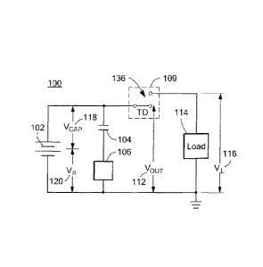
There is shown in Fig. 6 one embodiment of system 100 for regulating the
output of a high-voltage, high-power DC supply. System 100 includes high-
voltage
DC power supply 102 and storage capacitor 104. System 100 also includes at
least
one non-dissipative regulator, e.g., regulator 106. The at least one non-
dissipative
regulator may include a plurality of regulators, as discussed in further
detail below.
As defined herein, non-dissipative means dissipation is not inherently
required for
regulator 106 to operate. The switches and other components in regulator 106
may
dissipate a small amount of power. Regulator 106 preferably has an output
voltage
range less than the output voltage range of high-voltage DC power supply 102.
Regulator 106 includes internal storage, capacitance, and control circuit
configured to
maintain a desired high voltage output at a desired high voltage, VouT-112, on
load
114, as discussed in further detail below.
The inventors hereof realized that regulator 106 only needs enough authority
to
deal with the droop on capacitor 104. For example, if the droop of storage
capacitor
104 is 10%, regulator 106 needs only a 10% range, rather than operating with
the full
voltage capability provided by high-voltage DC power supply 102. This
minimizes
the cost and losses of regulator 106. In one example, as shown in Fig. 6,
storage
capacitor 104 and regulator 106 are connected in series and the series
combination is
CA 02897160 2015-07-03
WO 2014/113077
PCT/US2013/059145
14
connected in parallel with high-voltage DC power supply 102. In another
example, as
shown in Fig. 7A, high-voltage DC power supply 102 and storage capacitor 104
are
connected in parallel, and regulator 106 is connected in series with the
parallel
combination. In yet another example, as shown in Fig 7B, DC power supply 102
and
regulator 106 are connected in series, and the series combination is connected
in
parallel with storage capacitor 104. System 100, Figs. 6-7B, may also include
modulator 109 including at least one switching device 136, e.g., at least one
IGBT or
similar type device. In either case, as capacitor 104, Figs. 6-7B, discharges
during
pulsing, the output load voltage, VL-116 would droop without regulator 106.
Regulator 106 is configured to cancel this droop and produces a flat output
voltage,
VouT-112.
In one example, the variation in the output load voltage is cancelled by
measuring the actual load voltage, VL-116, comparing the actual load voltage
to the
desired high-voltage, and adjusting the actual load voltage to the desired
output by
adjusting regulator voltage, VR-120, such that the sum of the regulator
voltage, VR-
120, plus the storage capacitor voltage, Vc-I 18, equals the desired output
voltage.
Regulator 106 effectively gives system 100 an infinite capacitance because the
output voltage does not vary during the pulse or charging. One preferred
location of
regulator 106 is in series with the capacitor, as shown in Fig. 6. This
provides a flat
voltage to high-voltage DC power supply 102 as well as to load 114. As a
result,
high-voltage DC power supply 102 can operate at constant power as the
modulator is
pulsing, eliminating flicker. Such a design also allows high-voltage DC power
supply
102 to be SCR-controlled, which reduces cost when compared to a conventional
switching supply. The result is system 100 efficiently regulates the output of
high-
CA 02897160 2015-07-03
WO 2014/113077
PCT/US2013/059145
voltage, high-power DC supply 102 and significantly reduces droop.
One example of the output waveforms of system 100, Fig. 6 is discussed below
with reference to Fig. SA and 88. In this example. capacitor 104 is initially
charged to a
voltage higher than desired output voltage, as shown by trace 164, Fig. 8A.
Switch 136,
Fig 6. is closed at the beginning of the pulse, and regulator 106 initially
switches power
into its internal storage capacitance, producing a voltage that opposes the
voltage on
capacitor 104. The voltage on capacitor 104 droops, as shown at 166, Fig. 8A,
as energy
is delivered to load 114. As the voltage droops below the level of trace 172,
Fig. 8B,
regulator 106, Fig. 6, reverses power flow, switching power out of its
internal storage
capacitance, producing a voltage that adds to the voltage on capacitor 104.
The net
output voltage across load 114 is constant, as shown in trace170. Preferably,
the high
switching speed of regulator 106 allows this process to precisely regulate the
output
voltage throughout the pulse. The voltage of high-voltage DC power supply 102
is
constant, as shown by trace 180, Fig. 8B. Between pulses, storage capacitor
104. Fig. 6
is recharged and regulator 106 operates in reverse. Regulator 106 initially
adds, then
subtracts voltage on storage capacitor 104 allowing high-voltage DC power
supply 102
to operate at a nearly constant power level, e.g., as shown by trace 180, Fig.
8B. In one
example, the output voltage variation of system 100, Figs. 6-7B, is much less
than 1%.
Regulator 106 also allows for line voltage variations that are faster than can
be handled
by DC power supply 102. In one example, voltage regulator 106 needs to handle
only
about 7.5% of the voltage. The only net power required is to replace the
losses in the
regulator. Preferably, regulator 106 is very compact and less expensive
compared to a
typical 7 MW conventional inverter that would be required.
Regulator 106, Figs. 6-7B, is preferably based on a bridge circuit. One
CA 02897160 2015-07-03
WO 2014/113077
PCT/US2013/059145
16
implementation configured as a full-bridge single stage regulator 106 is shown
in Fig.
9A. Rectifier bridge circuit 155 preferably includes a full bridge of
switching
transistors, e.g., switching transistors A-157, B-159, C-161, and D-I63 as
shown that
produce the output. Rectifier bridge circuit 155 includes internal storage,
e.g., a
capacitance, such as capacitor 108, preferably charged by transformer 153, and
control
circuit 110 configured to maintain a desired high voltage output at a desired
high
voltage, VouT-112, Figs. 6-7B, on load 114. Preferably, output filter 165,
Fig. 9A,
removes the transient voltages.
Bridge circuit 155 preferably operates in four different modes. For example,
during pulsing, bridge circuit 155 subtracts, and then adds voltage to the
output.
During charging, bridge circuit 155 adds, and then subtracts voltage to the
output.
There are at least two ways bridge circuit 155 can be switched. One switching
duty
cycle is shown in Fig. 10. In this example, one switch, e.g., switch C-161,
Fig. 9A,
operates during the first half of the pulse. The duty factor of this switch
steadily
increases while the other switches are closed. At the midpoint of the pulse
this switch
is closed, and it remains closed for the rest of the pulse. The diagonally-
opposite
switch, e.g., switch B-159, then begins to operate with its duty steadily
increasing.
Switches 8-159, C-161 are then opened at the end of the pulse. During
charging, the
duty cycle is similar except that different switches operate; in this example,
switches
A-157 and D-163. The duty cycle for this exemplary operation is shown in Fig.
10.
An alternate switching duty cycle to regulate the output voltage of system
100,
shown in one or more of Figs. 6-7B, is shown in Fig. 11. The duty cycle in the
first
half of the pulse is the same as discussed above with reference to Fig. 10.
However,
in this example, the duty during the second half of the pulse changes: the
diagonally-
CA 02897160 2015-07-03
WO 2014/113077
PCT/US2013/059145
17
opposite switch closes, in this example, switch B-159, and the switch C-161
duty
goes to zero, then increases, as shown in Fig. 11. As in the previous example,
the
switching duty during charging is similar to the duty during pulsing.
The above descriptions are for the case when the transitions between switching
modes occur at the midpoint of the pulse, when the voltage on the main
capacitor has
drooped to half its maximum. This minimizes the bus capacitance needed.
However,
the mode transition can be made at any time, as long the mode transitions
during the
pulse and charge occur at the same capacitor droop voltage.
Regulator 106, Figs. 6-7B may be configured as a half bridge circuit 157, Fig.
9B, or as a four-switch half bridge circuit 159, Fig. 9C. Half bridge circuit
157, Fig.
9B, and four-switch half bridge circuit 159, Fig. 9C, also preferably include
internal
storage, e.g., capacitor 108, and control circuit 110 configured to maintain a
desired
high-voltage output at a desired high-voltage. Vo3T-112, Figs. 6-7B, on load
114.
Preferably, the transistors in half bridge circuit 157, Fig. 9B, four-switch
half bridge
circuit 159, Fig. 9C, and rectifier bridge circuit 155, Fig. 9A, are insulated
gate bipolar
transistors (IGBTs), e.g., as shown in Figs. 9A-9C. In other designs, the
transistors
used for rectifier bridge circuit 155, half bridge circuit 157, or four-switch
half bridge
circuit 159 may be field effect transistors (FETs), bipolar junction
transistors (BITs),
or similar type devices.
System 100, Fig. 12, for regulating the output of a high-voltage, high-power,
DC supply 102 where like parts include like numbers, preferably includes a
plurality
of regulators, e.g., regulators 106, 130, connected in series with capacitor
104 as
shown, or a plurality of a series of regulators as shown in Fig. 7A, to
provide greater
voltage regulation capability to system 100. In another example, system 100",
Fig 13,
CA 02897160 2015-07-03
WO 2014/113077
PCT/US2013/059145
18
includes a plurality of regulators, e.g., regulators 106, 130, connected in
parallel with
respect to each other and in series with capacitor 104 as shown to provide
greater
current capability to system 100. The plurality of regulators, or the
plurality of a
series of regulators, may also be connected in series with the parallel
combination of
high-voltage power supply 102, Fig. 7A, and storage capacitor 104, e.g., as
shown by
regulators 106 and 130 (shown in phantom). The plurality of regulators, or the
plurality of a series of regulators, may also be connected in series or in
parallel with
high-voltage power supply 102, Fig. 78, e.g., regulators 106 and 130 (shown in
phantom).
System 1001", Fig. 14, for regulating the output of a high-voltage, high-power
DC supply 102, may include transformer 230 as shown.
In one example, a plurality of storage capacitors 104 and a plurality of
regulators 106, may be integrated with pulse-step modulator 200, Fig. 15, or a
Marx
modulator 220, Fig. 16.
As discussed in the Background Section above, accelerators designed to
operate continuously may have a large amount of ripple because the high-
voltage
power supply is SCR-controlled. Although a switching supply would produce much
less ripple, it would be much more expensive.
Conventional approaches to mitigate the ripple from the power supply may
rely on a modulating-anode supply, which reduces the ripple voltage between
the
cathode and the modulating anode, and low-level RF feedback that compensates
for
the remaining ripple. Although this method is somewhat effective, it may be
necessary in some instances to reduce the ripple even further.
System 300, Figs. 17-19, for regulating the output of a high-voltage, high-
CA 02897160 2015-07-03
WO 2014/113077
PCT/US2013/059145
19
power DC supply includes high-voltage DC power supply 102, storage capacitor
104
and load 114. System 300 also includes at least one regulator 106, having the
same
structure as discussed above with reference to one or more of Figs. 6-13,
coupled in
series with any of high-voltage DC power supply 102, storage capacitor 104 and
load
114 to efficiently reduce DC ripple. Regulator 106 may be coupled in series
with
capacitor 104 as shown in Fig. 17, in series with high-voltage DC power supply
102
as shown in Fig. 18, or in series with the parallel combination of high-
voltage DC
power supply 102 and capacitor 104 as shown in Fig. 19. The location of
regulator
106 in continuous system 300 does not make any difference to the over-all
electrical
properties (unlike pulsed system 100 discussed above with reference to one or
more of
Figs. 6-13) because load 114 is constant and there is no flicker or droop.
In this example, regulator 106, Figs. 17-19 is preferably configured to reduce
DC ripple created by high-voltage DC power supply 102 by generating a
cancellation
voltage which approximately matches any ripple created by high-voltage DC
power
supply 102.
In one example, bridge circuit 155, Fig. 9, generates the cancellation voltage
which approximately matches any ripple on the high DC voltage created by DC
power
supply 102.
Although specific features of the invention are shown in some drawings and not
in others, this is for convenience only as each feature may be combined with
any or all
of the other features in accordance with the invention. The words "including",
"comprising", "having", and "with" as used herein are to be interpreted
broadly and
comprehensively and are not limited to any physical interconnection. Moreover,
any
embodiments disclosed in the subject application are not to be taken as the
only possible
CA 02897160 2015-07-03
WO 2014/113077
PCT/US2013/059145
embodiments.
What is claimed is: