Note: Descriptions are shown in the official language in which they were submitted.
CA 02897856 2016-08-08
275538
SENSOR DEVICES AND METHODS FOR USE
IN SENSING CURRENT THROUGH A CONDUCTOR
BACKGROUND OF THE INVENTION
[0002] The field of the invention relates generally to sensor devices and
methods and,
more particularly, sensing current through a conductor.
[0003] At least some known utility meters are used to measure electricity
supplied from
a power source to a user. To enable an amount of energy supplied to a user to
be accurately
measured, utility meters often include one or more sensor devices to sense
current flowing
through a conductor between the power source and the user. When included in a
utility
meter, the sensor device is intended to function accurately over an operating
range of
voltages and/or currents.
[0004] Various
types of known current sensor devices are used in utility meters. For
example, at least some known transformer sensor devices include a magnet core
with
magnet wire wound thereon to sense current flowing through a conductor.
Current sensor
devices including transformers, however, are generally known to be bulky and
expensive.
Current sensor devices with magnetic cores may be vulnerable to external
magnetic fields.
Exposure to external magnetic fields reduces the accuracy of magnetic core
current sensor
devices, and in some cases the accuracy may be reduced to the point where the
current
device registers only as little as 8% of the current that the current device
should be sensing.
Temperature cycles may also affect the magnetic core of current sensors and
cause
magnetic drift which reduces the accuracy of the current sensor.
-1-
CA 02897856 2015-07-16
275538
[00051 Another example of a known current sensor device is a Rogowski coil.
Rogowski coils include a coil and are generally smaller than transformer
sensor devices.
However, Rogowski coils are known to provide only limited accuracy during low
current
and/or high current conditions over a range of voltages. As
a result, during
manufacturing, utility meters with known Rogowski coils are often subjected to
multiple
calibration processes to minimize the effects of these inaccuracies. Although
these
repeated calibration processes may reduce the inaccuracies of such sensor
devices, the
processes also increase manufacturiag times and costs of the utility meters.
BRIEF DESCRIPTION OF THE INVENTION
[0006] In one embodiment, a utility meter for use in transmitting electrical
energy from
a power source to a user is provided. The utility meter includes a sensor
device
positionable at least partially around a conductor to sense current flowing
through the
conductor and to output a signal representative of the sensed current. The
sensor device
includes a non-magnetic substrate, a coil comprising a plurality of turns
wound about the
substrate where the coil defines an aperture through which the conductor is to
be
received, and a dielectric material having a dielectric constant and
positioned adjacent to
the coil and at least partially within the aperture such that the dielectric
material is
between the coil and the conductor when the conductor is received through the
aperture.
The utility meter also includes a meter control board in communication with
the sensor
device to receive the signal representative of the sensed current from the
sensor device
and to determine an amount of electricity transmitted through the conductor
from the
power source to the user over time. The dielectric constant of the dielectric
material is
selected to reduce a capacitive coupling between the coil and the conductor
and to
consequently reduce a sensitivity of the sensor device such that the meter
control board
comprises only one calibration coe,ficient for calibrating the sensor device
over a current
range, and wherein the current range is about 2.0A to about 25,000A.
[0007] In another embodiment, a method of fabricating a utility meter for use
in
transmitting electrical energy from a power source to a user is provided. The
method
-2-
CA 02897856 2015-07-16
275538
includes providing a sensor device positionable at least partially around a
conductor to
sense current flowing through the conductor and to output a signal
representative of the
sensed current. Providing the sensor device includes forming a coil comprising
a
plurality of turns wound about a non-magnetic substrate where the coil defines
an
aperture through which the conductor is to be received, and positioning a
dielectric
adjacent to the coil and at least partially within the aperture such that the
dielectric
material is between the coil and the conductor when the conductor is received
through the
aperture. The method also includes connecting a meter control board with the
sensor
device to receive the signal representative of the sensed current from the
sensor device
and to determine an amount of electricity transmitted through the conductor
from the
power source to the user over time, and selecting the dielectric material such
that a
dielectric constant of the dielectric material reduces a capacitive coupling
between the
coil and the conductor and consequently reduces a sensitivity of the sensor
device such
that the meter control board comprises only one calibration coefficient for
calibrating the
sensor device over a current range where the current range is about 2.0 A to
about 25,000
A.
BRIEF DESCRIPTION OF THE DRAWINGS
[0008] Fig. 1 is a block diagram of an exemplary utility meter including an
exemplary
sensor device.
[0009] Fig. 2 is a partially disassembled view of the sensor device shown in
Fig. 1.
[0010] Fig. 3 is a perspective view of the sensor device shown in Fig. 1.
[0011] Fig. 4 is a plan view of the sensor device shown in Fig. 1.
[0012] Fig. 5 is a perspective view of an exemplary substrate and coil used
with the
sensor device shown in Fig. 1.
[0013] Fig. 6 is a cross-sectional view of an exemplary bobbin that may be
used with
the sensor device shown in Fig. 1.
-3-
CA 02897856 2015-07-16
275538
[0014] Fig. 7 is a circuit diagram of an exemplary coil and shields that may
be used
with the sensor device shown in Fig. 1.
[0015] Fig. 8 is a perspective view of an exemplary sensor device including
four lead
wires.
[0016] Fig. 9 is a circuit diagram of an exemplary coil and shields that may
be used
with the sensor device shown in Fig. 8.
DETAILED DESCRIPTION OF THE INVENTION
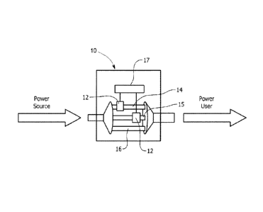
[0017] Fig. 1 illustrates a block diagram of an exemplary utility meter 10. In
the
exemplary embodiment, utility meter 10 includes a sensor device 12, a
conductor 14, and
a meter control board 17 coupled to sensor device 12. Conductor 14 may include
a bus
bar, multi-strand wire, single-strand wire, cable, or other suitable conductor
to transmit
electricity from a power source to a power user. The power source may include,
without
limitation, an electrical grid and/or a power generator system, such as a gas
turbine
engine, a hydroelectric turbine, a wind turbine, a solar panel, and/or another
suitable
generation and/or transmission system. The power source may also include a
smart-grid
in communication with meter control board 17. A user may include, without
limitation, a
residential user, a commercial user and/or any other user of electricity at
any level.
Sensor device 12 is coupled to conductor 14 to sense current flowing through
conductor
14. Sensor device 12 provides a signal representative of sensed current to
meter control
board 17. Based on the signal received from sensor device 12, meter control
board 17
determines an amount of electricity transmitted through conductor 14 from the
power
source to the user over time.
[0018] Because a charge may be incurred for electricity transferred from the
power
source to the user, it is desirable that sensor device 12 is highly accurate
to ensure the
user is charged substantially only :or electricity received, rather than being
charged for
substantially all the electricity transmitted to the user by the operator of
the power source.
-4-
CA 02897856 2015-07-16
275538
[0019] In this exemplary embodiment, utility meter 10 further includes
conductors 15
and 16 and another sensor device 12 coupled to conductor 15. It should be
appreciated
that any number of conductors and/or sensor devices (e.g., one, three, six,
etc.) may be
used in other utility meter embodiments. Moreover, it should be appreciated
that sensor
device 12 is not limited to only being used within utility meter 10, but may
be utilized in
virtually any application to sense current through a conductor, such as power
generation
applications, utility applications, automotive applications, appliance
applications,
telecommunication applications, etc.
[0020] Fig. 2 is a partially disassembled view of exemplary sensor device 12.
In the
exemplary embodiment, sensor dev: x 12 includes a substrate 102, a coil 104
including a
plurality of turns wound about substrate 102, and a dielectric material 108.
Coil 104
includes an aperture 110 defined therein, which is structured (e.g., by size,
orientation,
and/or shape, etc.) to receive conductor 14 therein. Dielectric material 108
is positioned
adjacent to coil 104 and at least partially within aperture 110. More
specifically, in this
embodiment, dielectric material 108 is positioned at least partially between
coil 104 and
conductor 14, when conductor 14 is positioned through aperture 110.
[0021] Dielectric material 108 may include one or more dielectric materials
having a
variety of characteristics configured in a variety of ways. For example,
dielectric
material 108 may have a dielectric constant equal to or greater than about 3.0
at about 10-
1000Hz. In some embodiments, the dielectric constant may be greater than about
3.5,
about 4.0, about 5.0, about 8.0, about 12.0, about 17.0 and/or any other
suitable dielectric
constant. In one exemplary embodiment, the dielectric constant of dielectric
material 108
may be approximately equal to about 3.5. In another exemplary embodiment, the
dielectric constant of dielectric material 108 may be approximately equal to
about 6Ø
[0022] Further, dielectric material 108 has at least one thickness, and may
have various
thicknesses. In the exemplary embodiment, dielectric material 108 positioned
adjacent to
coil 104 and at least partially withi - aperture 110 has a thickness of about
3.0 millimeters.
Also, in the same embodiment, dielectric material 108 positioned adjacent to
coil 104 but
-5-
CA 02897856 2015-07-16
275538
opposite aperture 110 has a thickness of about 1.2 millimeters. It should be
appreciated
that dielectric material 108 may have any thickness or thicknesses, that
enables sensor
device 12 to function as described herein. Generally, thickness of dielectric
material 108
is selected, at least partially based on the dielectric constant of dielectric
material 108, the
proximity of coil 104 to one or more conductors 14, 15 and 16, and/or space
available in
an intended environment for installation of the sensor device, etc. In some
example
embodiments, the thickness of dielectric material 108 may range from about 1.0
millimeter to about 3.0 centimeters, or greater in still other embodiments.
[0023] In the exemplary embodiment, dielectric material 108 may be fabricated
from
one or more of several types of material, such as, without limitation, plastic
materials,
thermoplastic materials, thermoset tyiaterials, ceramic materials, metallic
materials, wood
materials, clay materials, organic materials, any mixture thereof, and/or
other materials
suitable to perform as described herein. In the exemplary embodiment of Fig.
2,
dielectric material 108 includes a PBT thermoplastics material commercially
available
from a Valox family of materials. In various embodiments, dielectric material
108
includes one or more of, without limitation, Kapton tape, a polyvinylidene
fluoride
(PVDF) material, a room temperature vulcanized silicone (RTV) polymer, a PBT
thermoplastics material commercially available from a Valox family of
materials (e.g.,
Valox 365 or Valox V9561), a polyethylene terephthalate (PET) thermoplastic
material from the Rynite0 family of materials, a PPS thermoplastic material
commercially available from the Ryton0 family of materials, a PPS
thermoplastic
material commercially available from the Primef0 family of materials, a nylon
thermoplastic material commercially available from the Zyte10, Stany10, or RTP
families of materials, a LCP thermoplastic material (e.g., Sumitomo E5008L or
E4008L
materials), etc. One or more types of dielectric material 108 may be selected
based on
dielectric constant, suitability for one or more manufacturing techniques,
dimensional
stability, cost, moldability, workability, rigidity, and/or other
characteristic of the
material(s). In at least one example, dielectric material 108 is selected at
least partially
based on the variability of its dielectric constant over temperature.
-6-
CA 02897856 2015-07-16
275538
[0024] Fig. 3 is a perspective view of sensor device 12 (shown as assembled)
with
conductor 14 extending through aperture 110. As described above, sensor device
12
senses current flow through conductor 14. Specifically, when current flows
through
conductor 14, a current is induced in coil 104. The amount of current induced
in coil 104
is representative of the amount of current flowing through conductor 14. When
sensor
device 12 is positioned around conductor 14, coil 104 is spaced a distance
from conductor
14. Accordingly, capacitance exists between coil 104 and conductor 14. The
capacitance
may affect the accuracy of sensor device 12 at different operating voltages
(e.g., a range
from about 30V to about 277V). In the exemplary embodiment, dielectric
material 108 is
positioned within at least a portion of an air-gap 106 defined between coil
104 and
conductor 14. As a result, dielectric material 108 affects and/or facilitates
a reduction of
the capacitance between coil 104 and conductor 14, while permitting coil 104
and
conductor 14 to remain in close proximity.
[0025] The reduction in capacitance enables sensor device 12 to sense current
flowing
through conductor 14 with improved accuracy, as compared to known Rogowski
coils or
other air-gap coils. More specifically, by reducing capacitance coupling
between coil
104 and conductor 14, the sensitivity to operating voltage is reduced. As a
result,
consistent current sensing is provided at different operating voltages across
a range of
different currents, including high and low currents. Accordingly, when sensor
device 12
is included in utility meter 10, one or more processes necessary for
calibrating known
sensor devices may be omitted. Specifically, in the exemplary embodiment, the
consistency of sensor device 12 to accurately detect current across different
operating
voltages may permit meter control board 17 to use only one calibration
coefficient for a
plurality of operating voltages, as compared to known utility meters, which
require
multiple calibration coefficients for use at different voltages. Moreover, the
reduction in
capacitance between coil 104 and conductor 14 not only facilitates reducing
and/or
simplifying the calibration processes, but also facilitates reducing
manufacturing cost,
resources, and/or time with at least the same and often improved accuracy
across
operating voltage/current ranges.
-7-
CA 02897856 2015-07-16
275538
[0026] As shown in Fig. 3, in this exemplary embodiment, sensor device 12
includes an
enclosure 112. Enclosure 112 may be formed from a variety of materials and/or
through
a variety of fabrication processes. In the exemplary embodiment, enclosure 112
includes
substantially only dielectric material 108, such that dielectric material 108
is positioned
about coil 104, opposite aperture 110. As such, when used within utility meter
10 having
three-phase conductors 14, 15, and 16, sensor device 12 may be positioned
about
conductors 14 and proximate to at least one other conductor 15 (as shown in
Fig. 1), and
potentially proximate to conductor 16. Similar to the interaction between coil
104 and
conductor 14, a capacitance exists between coil 104 and conductor 15, which
may
adversely affect and/or degrade the accuracy of sensor device 12. Due to the
position of
dielectric material 108 opposite aperture 110, dielectric material 108 is
positioned
between coil 104 and adjacent conductor 15. Accordingly, dielectric material
108 is
further provided to reduce capacitance between coil 104 and conductor 15. In
this
manner, sensor device 12 may provide improved accuracy when used in utility
meter 10
having multiple conductors and/or when used in close proximity to one or more
other
conductors, as compared to known air-gap coils.
[0027] In some embodiments, enclosure 112 may include one or more materials in
addition to dielectric material 108, such as non-dielectric materials or
dielectric materials
that have different characteristics. In one embodiment, enclosure 112 includes
dielectric
material 108 and an additive material, which is provided to support dielectric
material
108 in one or more locations relative to coil 104 to enable it to perform as
described
herein. The additive material may include plastic materials, thermoplastic
materials,
thermoset materials, ceramic materials, metallic materials, wood materials,
clay
materials, organic materials, any mixture thereof, and/or other suitable
materials. The
additive material may be selected based on manufacturing techniques,
dimensional
stability, cost, moldability, workability, rigidity, and/or other
characteristics of the
material, etc. In such embodiments, when dielectric material 108 is a higher
cost material
(as compared to the additive material), the inclusion of an additive material
may reduce
the overall cost of sensor device 12. Further, one or more additive materials
may be used
-8-
CA 02897856 2015-07-16
275538
to perform one or more additional functions, such as supporting dielectric
material 108,
protecting and/or insulating coil 104, etc. As should be apparent, the
additive material
may be used as part of enclosure 112 in various embodiments. In the exemplary
embodiment, however, an additive material is omitted, as enclosure 112
substantially
only includes dielectric material 108.
[0028] Enclosure 112 may be fabricated from the dielectric material, formed
integrally
from dielectric material 108 and at least one additive material, or assembled
from
separate dielectric material(s) 108 and additive material(s). Enclosure 112
and/or
dielectric material 108 may be fabricated using one or more injection molding
processes
and/or other suitable fabrication processes. In the exemplary embodiment,
enclosure 112
is constructed via a single injection molding process, in which dielectric
material 108 is
injected into a mold structured to form enclosure 112.
[0029] Alternatively, enclosure 112 may be constructed from a multi-stage
injection
molding process. In a multi -stage process, an additive material is molded
into a specific
shape through an initial molding process. Subsequently, the molded additive
material is
positioned within a mold, and dielectric material 108 is injected into the
mold. Dielectric
material 108 flows into voids defined between the mold and/or the additive
material, to
form enclosure 112 from dielectric material 108 and additive material. In
various
embodiments, a multi-stage molding process may permit a relatively high-cost
dielectric
material to be specifically positioned relative to coils 104 such that desired
performance
as described herein is achieved, while still permitting other portions of
enclosure 112 to
be constructed from one or more relatively low cost materials.
[0030] It should be appreciated that enclosure 112 may be constructed by other
fabrication techniques to provide dielectric material 108 throughout or at
desired
positions relative to coil 104 and/or conductor 14. In one example, dielectric
material
108 is constructed separately from an additive material, and subsequently
transformed
and/or constructed with the additive material to form enclosure 112. In yet
another
-9-
CA 02897856 2015-07-16
275538
example, a tubular dielectric material may be inserted into an aperture formed
by an
additive material to form enclosure 112.
[0031] In the exemplary embodiment, enclosure 112 includes a mount 116 that
defines
aperture 110. When conductor 14 is received in aperture 110 (as shown in Fig.
3), air-
gap 106 is formed between mount 116 and conductor 14. Simultaneously, a
friction fit is
created between mount 116 and conductor 14. Mount 116 may include dielectric
material 108 and/or another material. It should be appreciated that mount 116
may be
formed in a variety of different shapes that are designed to receive and/or
couple to
various types, shapes, and/or orientations of conductors. In at least one
embodiment,
mount 116 defines an aperture that is structured to form a friction fit with a
rectangular-
shaped bus bar conductor.
[0032] Referring again to Fig. 2, enclosure 112 includes a first portion 118
and a
second portion 120. First portion 118 is releasably coupled to second portion
120 such
that substrate 102 and coil 104 a substantially enclosed therein.
Specifically, when
assembled, as shown in Fig. 3, first portion 118 is coupled to second portion
120 through
at least one ship-lap joint to form enclosure 112. It should be appreciated
that first
portion 118 and second portion 120 may be coupled together through a variety
of
different methods, including, without limitation, one or more butt joints,
screw joints,
hinge joints, tab-slot arrangements, tongue-and-groove arrangements,
fasteners, etc.
While enclosure 112 has generally toroidal shape, as shown in Fig. 3, it
should be
appreciated that other enclosure embodiments may define any shape and/or size,
that is
sized and/or operates to at least partially enclose substrate 102, coil 104
and/or shields,
and that enables dielectric material 108 to perform as described herein.
[0033] Further, in the exemplary embodiment, the thickness of dielectric
material 108
varies throughout enclosure 112. The ship-lap joint between first portion 118
and second
portion 120 provides an overlap of first portion 118 and second portion 120.
Specifically,
in this exemplary embodiment, first portion 118 and second portion 120 each
have a
thickness of about 1.2 millimeters at aperture 110. When the first portion 118
and the
-10-
CA 02897856 2015-07-16
275538
second portion 120 are assembled, first portion 118 and second portion 120 at
least
partially overlap at the ship-lap joint (along aperture 110) to create a total
thickness of
about 2.4 millimeters. Moreover, in this exemplary embodiment, first portion
118 and
second portion 120 are structured such that the total thickness about the
outside of
enclosure 112 at a minor ship-lap joint (opposite aperture 110) is less than
about 1.2
millimeters. It should be appreciated that various methods of forming
enclosure 112 may
be used to provide one or more different thicknesses of enclosure 112 and/or
dielectric
material 108.
[0034] In various other embodiments, the thickness of enclosure 112 and/or
dielectric
material 108 may be between about 0.5 millimeters and about 3.0 centimeters.
In some
embodiments, one or more thicknesses of enclosure 112 and/or dielectric
material 108 are
between about 1.0 millimeters and 6.0 millimeters. Further, in various
embodiments, one
or more thicknesses of enclosure 112 and/or dielectric material 108 are
between about 1.0
millimeters and 4.0 millimeters. It should be appreciated that enclosure 112
and/or
dielectric material 108 may have different thickness in other embodiments,
potentially
based on a method of assembly/fabrication, the characteristic(s) of a selected
dielectric
material, and/or desired performance characteristic(s). Further, other shapes,
sizes,
and/or joints for enclosure 112 may be used to at least partially enclosure
coil 104, while
positioning dielectric material 108 relative to coil 104 to perform consistent
with one or
more aspects of the present disclosure.
[0035] In the exemplary embodiment, coil 104 includes an exemplary Rogowski
coil.
It should be appreciated, however, that sensor device 12 may include a coil
other than a
Rogowski coil. Further, aspects of the present disclosure are not limited to
only being
used with a Rogowski coil as described and illustrated herein.
[0036] Fig. 5 is a perspective view of substrate 102 and coil 104 separated
from
enclosure 112. In the exemplary embodiment, substrate 102 includes six bobbins
124,
126, 128, 130, 132, and 134 (collectively referred to as bobbins 124-134).
Each bobbin
124-134 has a substantially circular cross-section, and more particular, is a
right cylinder
-11-
'
CA 02897856 2015-07-16
275538
that includes flanges 135 at opposite ends that retain coil 104. In other
embodiments,
substrate 102 may have a different number, shape, and/or size of bobbins. For
example,
substrate 102 may include five bobbins, eight bobbins, ten bobbins, thirty
bobbins, or
another even or odd number of bobbins. Further, substrate 102 may include
bobbins
having a different shape, and/or an ovular cross-section, an elliptical cross-
section, or
rectangular cross-section, etc. In still other embodiments, substrate 102 may
include a
different structure for supporting coil 104, in addition to or other than
flanges 135. In at
least one embodiment, coil 104 is sufficient rigid to omit substrate 102.
[0037] In the exemplary embodiment, bobbins 124-134 are coupled together via
hinged
joints 137. More specifically, bobbins 124 and 126 are hingedly coupled to
permit
pivotal movement therebetween. In various embodiments, bobbins 124-134 may be
linearly aligned to enable efficient winding of coil 104 and/or pivoted
relative to one
another to form a substantially circular shape, as illustrated in Fig. 5.
[0038] Each of bobbins 124-134 of substrate 102 is a non-magnetic structure,
such that
bobbins 124-134 are constructed from one or more non-magnetic materials,
including, for
example, thermoplastic material, ..,ramic material, wood, material, or other
kinds of
suitable material(s). In this exemplary embodiment, each of bobbins 124-134 is
fabricated from a dielectric material, potentially consistent with dielectric
material 108.
By use of a non-magnet substrate 102, cost savings may be realized over known
sensor
devices that include one or more magnetic cores. Moreover, in the exemplary
embodiment, substrate 102 is shaped and/or sized to provide improved mounting
within
utility meter 10 and/or to a meter control board 17, as compared to known
sensor devices
that include bulky magnetic cores. Further, in this exemplary embodiment,
bobbins 124-
134 are formed separate from enclosure 112. It should be appreciated, however,
that
bobbins 124-134 may be formed integrally with and/or form one or more portions
of
enclosure 112 in other sensor device embodiments.
[0039] In the exemplary embodiment, coil 104 is wound multiple turns on each
bobbin
124-134. More specifically, in the exemplary embodiment, coil 104 includes a
single
-12-
CA 02897856 2015-07-16
275538
magnet wire that enables coil 104 to be wound from bobbin 124 to bobbin 134
with
several turns on each bobbin 124-134, and then wound back to bobbin 124 with
additional turns on each bobbin 124-134. It should be appreciated that, in
other
embodiments, other different winding patterns on bobbins 124-134 may be used.
Consistent with the above winding pattern across bobbins 124-134, a first end
and a
second end of coil 104 terminates at bobbin 124. The first end of coil 104 is
terminated
at lead wire 136, and the second end of coil 104 is terminated at lead wire
138, as shown
in Fig. 7, described further below.
[0040] In addition to coil 104, in the exemplary embodiment, one or more
shields are
applied to substrate 102. Specifically, Fig. 6 illustrates a partial cross-
sectional view of
sensor device 12 at bobbin 124. In the exemplary embodiment, bobbin 124
includes a
first shield 140 and a second shield 142. First shield 140 is positioned
between bobbin
124 and coil 104. Second shield 142 is positioned adjacent to coil 104 and
opposite from
first shield 140, such that coil 104 is positioned between first shield 140
and second
shield 142. Each bobbin 124-134 includes substantially the same shield-coil-
shield
pattern as shown in Fig. 6. In other embodiments, bobbins 124-134 may include
other
winding patterns, including winding patterns, in which the winding pattern
varies from
one bobbin to another bobbin.
[0041] In the exemplary embodiment, each shield 140 and 142 provides a Faraday
shield. More specifically, in this exemplary embodiment, first and second
shields 140
and 142 behave substantially consistent with a Faraday cage, in order to
facilitate
reducing common mode noise on the sensor device 12 and/or to provide a low-
pass filter
for high frequency noise filtering. As a result, first and second shield 140
and 142
facilitate improved performance in the context of one or more industry
standards for
electromagnetic interface (EMI) and/or eelectromagnetic compatibility (EMC).
[0042] During fabrication, a plurality of turns of a magnet wire are wound on
each
bobbin 124-134 from bobbin 124 to bobbin 134 to form first shield 140. Coil
104 is then
wound from bobbin 124 to bobbin 134 and back to bobbin 124 as described above.
-13-
=
CA 02897856 2015-07-16
275538
Subsequently, the magnet wire of first shield 140 is wound from bobbin 134
back to
bobbin 124 with a plurality of turns on each bobbin 124-134 to form second
shield 142.
As such, in the exemplary embodiment, first shield 140 and second shield 142
are formed
from a single magnet wire. The single magnet wire includes two ends, which may
be
terminated together, coupled to lead wire 138, and/or coupled to one or more
additional
lead wires, as described below. It should be appreciated that first shield 140
and second
shield 142 may include any suitable materials, such as, without limitation,
copper,
aluminum or other nonferrous conducting material. More generally, the
shielding
material may be formed as a sheet, a tape, a wire, a spray and/or any other
form that
enables bobbins 124-134 to include shields 140 and 142. As such, application
of shields
140 and/or 142 may be formed, without limitation, via winding, wrapping,
and/or
spraying, for example. In various embodiments, first and second shield 140 and
142 may
be formed separately from coil 104 and subsequently applied to coil 104.
[0043] Referring again to Fig. 5, sensor device 12 includes three lead wires
136, 138,
and 144 extending therefrom. Fig. 7 illustrates a circuit diagram of the
coupling of lead
wires 136, 138, and 144. Specifically, in the exemplary embodiment, first and
second
shields 140 and 142 are formed from a single magnet wire, with each end
coupled
together and coupled to lead wire 144. Further, the first end of coil 104
(formed from a
single magnet wire) is coupled to lead wire 136, and a second end of coil 104
is coupled
to lead wire 138. As shown in Fig. 5, lead wires 136, 138, and 140 extend from
enclosure
112 and form a twisted wire set. As such, lead wire 144 behaves as a low pass
filter
element to inhibit noise from first shield 140 and/or second shield 142 from
being
injected into a return path of the current signal provided by sensor device
12. The twisted
wire set has a length of at least about 0.25 inches. In other embodiments,
twisted wire set
may have a length of at least about 1.0 inches, or a length of at least about
3.0 inches. In
further embodiments, twisted wire set may have a length of at least about 6.0
inches. It
should be appreciated that other lengths of lead wires and/or twisted wire
sets may be
employed in other sensor device embodiments, possibly based on the performance
of the
-14-
CA 02897856 2015-07-16
275538
lead wire and/or twisted wire set to function as a filter to inhibit the
injection of noise into
a current signal transmitted from sensor device 12.
[0044] Figs. 8-9 illustrates another exemplary sensor device 200. In the
exemplary
embodiment, sensor device 200 includes a coil 204 and first and second shields
240 and
242, which are substantially consistent with coil 104 and shields 140 and 142
described
above. Sensor device 200, however, includes four lead wires 236, 238, 244, and
245.
Specifically, each end of the magnet wire forming first shield 240 and second
shield 242
are coupled to separate lead wires 244 and 245 to create a filter element.
Additionally, in
this exemplary embodiment, two lead wires 236 and 238 coupled to coil 204. As
illustrated in Fig. 8, lead wires 236, 238, 244, and 245 form a twisted wire
set, which
functions substantially consistent with the twisted wire set described above
with reference
to Fig. 5.
[0045] When coupled to meter control board 17, each lead wire 244 and 245 may
be
coupled together and coupled to lead wire 238. In some embodiments, twisted
lead wires
244 and 245 may behave as a filter element. Additionally, or alternatively, a
filter
element may be coupled between lead wires 244 and 245 and lead wire 238. Such
filter
elements may include, without limitation, a resistor-capacitor circuit, an
inductor-
capacitor circuit, a resistor-inductor circuit, and/or a resistor-inductor-
capacitor circuit.
[0046] Referring again to Figs. 3 and 7, in yet another embodiment, each end
of the
magnet wire forming shields 140 and 142 may be coupled together and coupled to
lead
wire 138 (i.e., one end of coil 104), rather than a separate lead wire 144. In
such an
exemplary embodiment, sensor device 12 may include lead wires 136 and 138,
while
omitting lead wire 144, thereby providing a two-wire sensor device 12. In the
exemplary
embodiment, some noise from first shield 140 and/or second shield 142 may be
injected
into the return path of a current signal provided from sensor device 12, while
providing
sufficient accuracy and/or repeatability for a desired operating environment.
In still other
embodiments, lead wires may be omitted from a sensor device embodiment to
provide for
mounting on a circuit board, such as meter control board 17. In such an
embodiment, a
-15-
CA 02897856 2015-07-16
275538
filter element may be provided by traces on meter control board 17, with a
sufficient
length to perform as described above with reference to lead wire 144.
Additionally, or
alternatively, filter element may include a resistor-capacitor circuit, an
inductor-capacitor
circuit, a resistor-inductor circuit, and/or a resistor-inductor-capacitor
circuit, to inhibit
noise from first shield 140 and/or second shield 142 from being injected into
a return path
for the current signal provided by sensor device 12.
[0047] In the exemplary embodiment, sensor device 12 is operational between
about
10Hz to about 1000Hz, and is substantially immune to signals outside this
range. More
specifically, conductor 14 may act as an antenna to pick up radio frequency
(RF) signals
and re-radiate the unwanted noise to sensor device 12. First and second shield
140 and
142 perform as a low-pass filter to inhibit injection of noise signals to
provide a high
signal-to-noise-ratio (SNR) output. More particularly, first and second
shields 140 and
142 reject re-radiated RF signal (and/or other noise signals) to provide a
high SNR for the
output of sensor device 12 when sensing low current through conductor 14. By
reducing
the effect of noise on current signals, the effective current sensing range of
sensor device
12, within applicable standards, is broader, as compared to known sensor
devices. In the
exemplary embodiment, first and second shields 140 and 142 may permit one or
more
additional filter elements (for low and/or high current performance) to be
omitted.
[0048] Moreover, first and second shields 140 and 142 substantially inhibit
EMI from
affecting the accuracy of sensor device 12. More specifically, first and
second shields
140 and 142 facilitate inhibiting the effects of EMI sources positioned
adjacent to sensor
device 12, such as adjacent electronics and/or devices intended to interfere
with the
accuracy of sensor device 12 and/or utility meter 10. Additionally, by
omitting a
magnetic core, as compared to known sensors, sensor device 12 provides
enhanced
immunity to EMI affects on accuracy. As such, sensor device 12 provides a more
robust
and/or accurate current sensor device, as compared to other known sensor
devices in the
presence of one or more EMI sources.
-16-
CA 02897856 2015-07-16
275538
[0049] Accuracy of sensor device 12 may be understood as a percentage of the
actual
value of current flowing through conductor 14. In the exemplary embodiment,
sensor
device 12 performs within about 0.2% of the actual value in the range between
about 2
amps and about 200 amps. More specifically, sensor device 12 performs within
Class
0.2, 0.1A to 200A at an operating voltage of between about 60V and about 600V,
more
specifically at about 240V, within an accuracy of 0.2%. It should be
appreciated that
sensor device 12 consistent with one or more aspects of the present disclosure
may
conform to one or more different accuracy standards at different operating
currents/voltages, possibly depending on the intended application and/or one
or more
accuracy requirements associated with the intended application.
[0050] Various methods are described herein for fabricating a sensor device
for
sensing current through a conductor. While these methods are described below
with
reference to sensor device 12, it should be understood that the methods are
not limited to
sensor device 12 and may be utilized to fabricate other sensor device
embodiments.
Likewise, sensor device 12 and sensor device 200 may be fabricated from
methods other
than those described below.
[0051] One exemplary method of fabricating sensor device 12 for sensing
current
through a conductor 14 includes providing coil 104 with a plurality of turns
about non-
magnetic substrate 102 and positioning dielectric material 108 adjacent to
coil 104, such
that when conductor 14 is disposed within aperture 110 defined by sensor
device 12,
dielectric material 108 is positioned between conductor 14 and coil 104. In
several
embodiments, the exemplary method may include at least partially and/or
substantially
enclosing coil 104 and/or substrate 102 within enclosure 112.
[0052] Another exemplary method of fabricating sensor device 12 for sensing
current
through conductor 14 includes providing Rogowski coil 104 and at least
partially
enclosing Rogowski coil 104 within dielectric material 108 such that, when
Rogowski
coil 104 is disposed about conductor 14, dielectric material 108 is disposed
between
Rogowski coil 104 and the conductor 14. Dielectric material 108 has a
dielectric constant
-17-
CA 02897856 2015-07-16
275538
of greater than or equal to about 3.5. In several embodiments, the exemplary
method
may include assembling a first portion of an enclosure and a second portion of
the
enclosure with the Rogowski coil disposed therebetween to at least partially
enclose the
Rogowski coil. The enclosure includes the dielectric material. Additionally,
or
alternatively, the exemplary method may include forming the Rogowski coil on a
substrate having a plurality of thermoplastic bobbins. Further, the exemplary
method
may include forming the plurality of thermoplastic bobbins from a dielectric
material.
[0053] Yet another exemplary method of fabricating a sensor device 12 for
sensing
current through a conductor 14 includes winding a first shield of a magnet
wire about
each of a plurality of bobbins of a substrate, winding a coil about each of
the plurality of
bobbins of the substrate, and winding a second shield of magnet wire about
each of the
plurality of bobbins of the substrate.
[0054] Referring to sensor device 12 of Fig. 3, for example, the exemplary
method may
include coupling a first end and a second end of the magnet wire to a
reference lead 144
of sensor device 12, coupling a first end of the coil to a first lead 136 of
sensor device 12,
and coupling a second end of the coil to a second lead 138 of sensor device
12. Further,
the exemplary method may include at least partially enclosing the coil and the
first and
second shield within an enclosure, the enclosure comprising at least one
dielectric
material.
[0055] Another exemplary method of fabricating a sensor device 12 for sensing
current
through a conductor 14 includes providing sensor device 12 including non-
magnetic
substrate 102 defining aperture 110, coil 104 having a plurality of coil turns
about at least
a portion of non-magnetic substrgte 102, first shield 140 disposed between
each of
substrate 102 and the plurality of coil turns, second shield 142 disposed
proximate to the
plurality of coil turns, opposite first shield 140. The exemplary method also
includes
coupling lead wire 144 to at least one of first shield 140 and second shield
142, coupling
lead wire 136 to a first end of coil 104, coupling lead wire 138 to a second
end of coil
104, and forming a twisted set of lead wires from lead wires 136, 138 and 144.
-18-
CA 02897856 2015-07-16
275538
[0056] In various embodiment, coupling lead wire 144 to at least one of first
shield 140
and second shield 142 includes coupling lead wire 144 to each of the first
shield 140 and
second shield 142. In other embodiments, coupling lead wire to at least one of
first shield
and second shield includes coupling lead wire 244 to first shield 140 and
coupling a lead
wire 245 to second shield 142.
[0057] As shown in FIG. 5, coil 104 wraps around substrate 102 in the form of
bobbins
124-134. In the exemplary embodiment, each bobbin 124-134 is toroidal and
includes a
circular area around which coil 104 is wrapped. The core of each bobbin 124-
134 is an
air core. Unlike the previously disclosed magnetic core current sensor
devices, the air
core of coil 104 does not become saturated. Tests have shown that the
disclosed air core
coil 104 is accurate at 0.4% from 10 milliamperes to 25,000 amperes. At lower
currents, i.e., less than 1,000 Amps, the accuracy of sensor device 12 is
0.2%, while at
higher currents, i.e., greater than 10,000 Amps, the accuracy lowers to 0.4%.
At those
higher currents, conductors 14, 15, and 16 interact with each other and
function as
parallel plate capacitors, affecting the accuracy of sensor device 12. Sensor
device 12 is
an inductor with no core to saturate; therefore, sensor device 12 can work
continuously as
an inductor without the possibility of saturation or oversaturation.
[0058] As an inductor with an air core, sensor device 12 is voltage
independent.
Whereas a traditional current transformer may burn out at high voltages,
sensor device 12
is able to read the current through conductor 14 independent of what voltage
is passing
through conductor 14. Voltage does not affect the operation of coil 104.
Voltage is also
not measured by sensor device 12 and rather is measured at a different
location in the
power delivery system.
[0059] Although in the exemplary embodiment, sensor device 12 is described as
being
operational between about 10Hz tu about 1000Hz, it should be appreciated that
the air
core enables sensor device 12 to operate outside of that range as well. It
should also be
appreciated that utility meter 10, may include multiple sensor devices 12
measuring
multiple different conductors. For example, in another exemplary utility meter
10,
-19-
CA 02897856 2015-07-16
275538
conductors 14, 15, and 16 may each be enclosed by a different sensor device
12. One
or more of the above described embodiments provide a highly-accurate sensor
device.
More specifically, the sensor devices, utility meters, and methods described
herein may
provide a highly-accurate sensor device that provides an expanded operating
range with
reduced calibration requirements over known coil sensors. For example, the
disclosed
dielectric material may provide reduced capacitance between a coil and one or
more
conductors, thereby providing improved accuracy across a range of currents
and/or
voltages. The improved accuracy may be realized with fewer calibration
processes
during manufacturing, resulting in reduced manufacturing cost and/or time. In
another
example, the disclosed shielding techniques provide improved rejection of EMI,
originating from other electronics and/or tampering devices.
[0060] Although specific features of various embodiments of the invention may
be
shown in some drawings and not in others, this is for convenience only. In
accordance
with the principles of the invention, any feature of a drawing may be
referenced and/or
claimed in combination with any feature of any other drawing.
[0061] While there have been described herein what are considered to be
preferred and
exemplary embodiments of the present invention, other modifications of these
embodiments falling within the scope of the invention described herein shall
be apparent
to those skilled in the art.
-20-