Note: Descriptions are shown in the official language in which they were submitted.
CA 02898453 2015-07-16
WO 2014/142841
PCT/US2013/030940
MULTILAYER FLUIDIC DEVICES AND METHODS FOR THEIR
FABRICATION
BACKGROUND
This disclosure relates generally to fluidic devices used for analytical and
synthetic chemistry, and more specifically to flowcells used for sequencing
and
other analyses of nucleic acid arrays.
Biological arrays have become a key tool for genomic analysis in research
settings and arc poised to become important tools in clinical settings for
diagnosing
human disease. In certain applications, individual DNA probes are attached to
a
geometric grid on an array support. A test sample, such as from a known person
or
organism, is exposed to the grid, such that complimentary gene fragments bind
to
probes at known locations on the array. Alternatively, a test sample, such as
from a
known person or organism, can be attached to the support and evaluated, for
example, using a DNA sequencing technique. In either format the array can be
detected, for example, using fluorescent reagents delivered fluidically to the
array
surface. Often the techniques utilize multiple steps of fluid delivery and
multiple
detection steps. The need for precise fluidic manipulations and accurate high-
resolution detection in array techniques places big demands on arrays, the
materials
from which they arc made and the devices that house them.
Significant improvements have recently been made in the biochemical
assays that are run on arrays, the imaging systems used to detect the arrays
and the
data processing systems used to evaluate the results obtained from the arrays.
For
example, improvements in sequencing chemistry, imaging optics and sequence
data
analysis used in commercial sequencing platforms have resulted in faster, more
accurate and higher resolution genomic analysis than ever before. However, as
these improvements occur, the resulting increase in sequence platform usage
creates
increased demand for arrays and the flowcells that house them. Because arrays
and
flowcells are generally disposable, this demand scales directly with the
increased
demand for genomic analysis. Improvements in array and flowcell fabrication
are
needed to prevent the cost of their production from becoming an impediment to
reductions in the overall cost of genomic analyses. Furthermore, improvements
in
1
CA 02898453 2015-07-16
WO 2014/142841
PCT/US2013/030940
array and flowcell fabrication are also needed to avoid counteracting the
advances in
other components of genetic analysis platforms that are otherwise positioning
the
technology to become more clinically useful and widespread. The present
invention
satisfies these needs and provides other advantages as well.
BRIEF SUMMARY
The present disclosure provides a fluidic device including (a) an inorganic
solid support attached to an organic solid support by a bonding layer, wherein
the
inorganic solid support has a rigid structure and wherein the bonding layer
includes
a material that absorbs radiation at a wavelength that is transmitted by the
inorganic
solid support or the organic solid support, and (b) at least one channel
formed by the
attachment of the inorganic solid support to the organic solid support,
wherein the
channel is configured to contain a liquid and the bonding layer that attaches
the
inorganic solid support to the organic solid support provides a seal against
liquid
flow. In particular embodiments, the material that absorbs the radiation is
not an
electrically conductive material such as a metal.
This disclosure further provides a method for making a multilayer device.
The method can include the steps of (a) providing an inorganic solid support
and an
organic solid support, wherein the inorganic solid support has a rigid
structure; (b)
providing a radiation-absorbing material; (c) contacting the inorganic solid
support,
the organic solid support and the radiation-absorbing material in a
configuration
wherein the radiation-absorbing material is present at an interface between
the
inorganic solid support and the organic solid support; and (d) applying
compression
at the interface and irradiating the radiation-absorbing material with the
radiation to
form a bonding layer between the inorganic solid support and the organic solid
support. In particular embodiments, the radiation-absorbing material is not an
electrically conductive material such as a metal.
Also provided is a fluidic device having at least one channel defined by an
inorganic solid support attached to an organic solid support by a bonding
layer,
wherein the fluidic device is made by the process of: (a) contacting the
inorganic
solid support, the organic solid support and a radiation-absorbing material in
a
configuration wherein the radiation-absorbing material is present at an
interface
2
between the inorganic solid support and the organic solid support; and (b)
applying compression
at the interface and irradiating the radiation-absorbing material with the
radiation to form the
bonding layer between the inorganic solid support and the organic solid
support. In particular
embodiments, the radiation-absorbing material is not an electrically
conductive material such as
a metal.
The present disclosure provides various embodiments relating to a method for
making a
multilayer device, comprising (a) providing an inorganic solid support and an
organic solid
support, wherein the inorganic solid support comprises a rigid structure;
wherein the providing of
the inorganic solid support comprises creating a chemically reactive layer at
the surface of the
inorganic solid support; (b) providing a radiation-absorbing material, wherein
the radiation-
absorbing material is not a metal; (c) contacting the chemically reactive
layer of the inorganic
solid support, the organic solid support and the radiation-absorbing material
in a configuration
wherein the radiation-absorbing material is present at an interface between
the chemically
reactive layer of the inorganic solid support and the organic solid support;
and (d) applying
compression at the interface and irradiating the radiation-absorbing material
with the radiation
to form a bonding layer between the inorganic solid support and the organic
solid support;
wherein the multilayer device comprises a fluidic device having a channel
formed by attachment
of the inorganic solid support to the organic solid support.
The present disclosure provides various embodiments relating to a fluidic
device
comprising (a) an inorganic solid support, including at the surface a
chemically reactive layer,
said inorganic solid support attached to an organic solid support by a bonding
layer, wherein the
inorganic solid support has a rigid structure and wherein the bonding layer
comprises a material
that absorbs radiation at a wavelength that is transmitted by the inorganic
solid support or the
organic solid support, wherein the material that absorbs the radiation is not
a metal, and (b) at
least one channel formed by the attachment of the inorganic solid support to
the organic solid
support, wherein the channel is configured to contain a liquid and the bonding
layer that attaches
the inorganic solid support to the organic solid support provides a seal
against liquid flow.
3
CA 2898453 2019-09-06
BRIEF DESCRIPTION OF THE DRAWINGS
Figure 1 shows profile views of multilayer fluidic devices undergoing a laser
induced
bonding process, wherein Panel A shows a device formed by in organic layer
sandwiched
between two inorganic layers and Panel B shows a device formed by a single
organic layer
bonded to a single inorganic layer.
Figure 2 shows a diagrammatic representation of a process for fabricating a
multilayer
flowcell.
Figure 3 shows (a) Activation of ITO on D263 surface using Oxygen plasma (b)
Surface
functionalization of ITO with APTMS and (c) IR bonding of black polyimide to
silanized
surface.
Figure 4 shows a photograph of a flowcell having top and bottom surfaces with
ITO
layers that are each connected to a pair of electrical contacts.
Figure 5 shows a diagram in which input and output devices are electrically
connected to
pairs of electrical contacts of the flowcell of Fig. 4.
DETAILED DESCRIPTION
Terms used herein will be understood to take on their ordinary meaning in the
relevant art
unless specified otherwise. Several terms used herein and their meanings are
set forth below.
As used herein, the term "array" refers to a population of sites that can be
differentiated
from each other according to relative location. Different molecules that are
at different sites of an
array can be differentiated from each other according to the locations of the
sites in the array. An
individual site of an array can include one or more molecules of a particular
type. For example, a
site can include a single target nucleic acid molecule having a particular
sequence or a site can
include
3a
CA 2898453 2019-09-06
CA 02898453 2015-07-16
WO 2014/142841
PCT/US2013/030940
several nucleic acid molecules having the same sequence (and/or complementary
sequence, thereof). The sites of an array can be different features located on
the
same substrate. Exemplary features include without limitation, wells in a
substrate,
beads (or other particles) in or on a substrate, projections from a substrate,
electrodes on a substrate, metal pads on a substrate, gel pads on a substrate,
ridges
on a substrate or channels in a substrate. The sites of an array can be
separate
substrates each bearing a different molecule. Different molecules attached to
separate substrates can be identified according to the locations of the
substrates on a
surface to which the substrates are associated. Exemplary arrays in which
separate
substrates are located on a surface include, without limitation, those having
beads in
wells.
As used herein, the term "bonding layer" refers to an area that attaches two
support structures to each other. For example, the bonding layer can include
one or
more covalent or non-covalent bonds that form the attachment. A covalent bond
is
characterized by the sharing of pairs of electrons between atoms. A chain of
two or
more covalent bonds can form a molecular link between two support structures.
Thus, the bonding layer can have a thickness of one or more covalent bond-
lengths.
In particular embodiments, each molecular link can span the bonding layer
uninterrupted by any non-covalent bonds. Alternatively, a molecular link can
include one or more non-covalent bonds in a chain of bonds that span the
bonding
layer. A non-covalent bond is a chemical bond that does not involve the
sharing of
pairs of electrons and can include, for example, hydrogen bonds, ionic bonds,
van
der Waals forces, hydrophilic interactions and hydrophobic interactions. In at
least
some embodiments, the bonding layer can include a combination of covalent
molecular links that span the bonding layer and non-covalent linkages that
span at
least part of the bonding area. Any of a variety of materials that join,
fasten, adhere,
connect or bind the solid supports can be included in a bonding layer.
Preferably a
bonding layer prevents fluid leakage by forming a seal.
As used herein, the term "channel" refers to an elongated passage that is
configured to contain a fluid or direct the flow of a fluid in or on a solid
support. An
example is an open channel configured as a groove, trench, straight, furrow or
the
like. The transverse cross section of an open channel can be, for example, U-
shaped, V-shaped, curved, angular, polygonal, or hyperbolic. Another example
is a
4
closed channel configured as a pipe, tube, tunnel or the like. A closed
channel can
have a circular, elliptical, square, rectangular, or polygonal cross section.
As used herein, the term "chemically reactive layer" refers to a surface
coating or region between surfaces that contains at least one moiety that is
capable
of becoming covalently modified or covalently attached to at least one other
moiety
upon physical or chemical stimulation. In some embodiments the region between
the
surfaces can be occupied by a liquid, gas, solid or plasma that contains the
reactive
moiety.
As used herein, the term "compression" refers to a force that brings two
objects together. For example, two solid supports can be brought together by
clamping the supports to each other, pressing the two supports together,
placing one
support atop another in a gravitational field (e.g. under earth's gravity or
centrifugally induced gravity) or the like.
As used herein, the term "each," when used in reference to a collection of
items, is intended to identify an individual item in the collection but does
not
necessarily refer to every item in the collection. Exceptions can occur if
explicit
disclosure or context clearly dictates otherwise.
As used herein, the term "gel" refers to a semi-rigid material that is
permeable to liquids and gases. Typically, gel material can swell when liquid
is
taken up and can contract when liquid is removed by drying. Exemplary gels
include, but are not limited to those having a colloidal structure, such as
agarose;
polymer mesh structure, such as gelatin; or cross-linked polymer structure,
such as
polyacrylamide, SFATM (see, for example, US Pat. App. Pub. No. 2011/0059865
Al) or PAZAMTm (see, for example, US Pat.
App. Ser. No. 13/784,368). Particularly
useful gel material will conform to the shape of a surface, for example, to
enter pits,
wells, or other concave features on the surface.
As used herein, the term "inorganic solid support" refers to a substrate
having an internal structure held together by bonds between inorganic atoms.
An
inorganic solid support can, however, have an organic layer on the surface of
the
substrate. A trace or small amount of organic matter can occur in the internal
structure of the inorganic solid support so long as the structural integrity
is primarily
mediated by bonds and interactions between inorganic atoms. Exemplary
inorganic
5
CA 2898453 2019-09-06
solid supports include, but are not limited to, glass and modified or
functionalized
glass, ceramics, silica or silica-based materials including silicon and
modified
silicon, metals, and optical fiber bundles.
As used herein, the term "interface" refers to a region at the boundary of two
materials. For example, the term can refer to an area between two solid
supports,
between a solid support and a chemically reactive layer, between chemically
reactive layers on two solid supports, between a bonding layer and a solid
support,
etc. The term can further refer to the surface of one or both of the materials
that
occur at the boundary. For example, the term can refer to a layer that is
present on
the surface of one or both materials.
As used herein, the term "organic solid support" refers to a substrate having
an internal structure that is held together by bonding between organic atoms
or
molecules. An organic solid support can, however, have one or more inorganic
atoms in the internal structure or on the surface of the substrate. For
example, a
trace or small amount of inorganic matter can occur in the internal structure
of the
organic solid support. Exemplary materials for organic solid supports include,
but
are not limited to, plastics, thermoplastics, thermosets, nylon, cyclic olefin
copolymers (e.g. ZeonorTm), cyclic olefin polymers, carbon fiber, and
polymers.
Exemplary thermoplastics include polyacrylate, polyamide, polyimide (e.g.
KaptonTM
products from DuPont), polybutylene terephthalate, polycarbonate, polyether
ketone, polyethylene, polyphenylene sulfide, polyacetal, polypropylene,
polystyrene,
polysulfone, polyvinyl butyral and polyvinyl chloride. Thermoplastics are
particularly useful of which KaptonTM KJ and black KaptonTM KJ are examples.
As used herein, the term "planar surface" refers to an external part or
external layer of a solid support that is apparently flat. Flatness can be
apparent to
the naked eye or at a magnification level of at most 5x, 10x, 100x, or 1000x.
The
planar surface can be on a portion of a substrate that otherwise has features
such as
wells, pits, metal features, gel features, channels, ridges, raised regions,
pegs, posts
or the like.
As used herein, the term "rigid structure" refers to a substrate that is stiff
or
inflexible. The rigid structure can optionally be capable of taking up a
liquid (e.g.
due to porosity) but will typically not swell substantially when taking up the
liquid
and will not contract substantially when the liquid is removed by drying.
6
CA 2898453 2019-09-06
=
As used herein, the term "solid support" refers to a substrate that is
insoluble
in aqueous liquid. The substrate can be non-porous or porous. The solid
support
can be rigid or flexible. A nonporous solid support is generally provides a
seal
against bulk flow of liquids or gases. Exemplary solid supports include, but
are not
limited to, glass and modified or functionalized glass, plastics (including
acrylics,
polystyrene and copolymers of styrene and other materials, polypropylene,
polyethylene, polybutylene, polyurethanes, TeflonTm, cyclic olefins,
polyimides
etc.), nylon, ceramics, resins, ZeonorTm, silica or silica-based materials
including
silicon and modified silicon, carbon, metals, inorganic glasses, optical fiber
bundles,
and polymers. Particularly useful solid supports for some embodiments have at
least
one surface located within a flowed! apparatus. Exemplary flowcells are set
forth in
further detail below.
The embodiments set forth below and recited in the claims can be understood
in view of the above definitions.
This disclosure provides a method for making a multilayer device. The
method can include the steps of (a) providing an inorganic solid support and
an
organic solid support, wherein the inorganic solid support has a rigid
structure; (b)
providing a radiation-absorbing material; (c) contacting the inorganic solid
support,
the organic solid support and the radiation-absorbing material in a
configuration
wherein the radiation-absorbing material is present at an interface between
the
inorganic solid support and the organic solid support; and (d) applying
compression
at the interface and irradiating the radiation-absorbing material with the
radiation to
form a bonding layer between the inorganic solid support and the organic solid
support. In particular embodiments, the radiation-absorbing material is not an
electrically conductive material. For example, in some embodiments, the
radiation-
absorbing material is not a metal.
In some embodiments, the above method can be used to create a device with
open channels, reservoirs or other features. Optionally, a device can be
fabricated to
have channels, reservoirs or other features that are enclosed. For example,
the
method for making a multilayer device can, optionally, further include the
steps of
(e) providing a second inorganic solid support; (0 contacting the second
inorganic
solid support with the organic solid support in a configuration wherein the
radiation-
absorbing material is present at a second interface between the second
inorganic
7
CA 2898453 2019-09-06
CA 02898453 2015-07-16
WO 2014/142841
PCT/US2013/030940
solid support and the organic solid support; and (g) applying compression at
the
second interface and irradiating the radiation-absorbing material with the
radiation
to form a bonding layer between the second inorganic solid support and the
organic
solid support. Whether or not the device includes enclosed features, steps (e)
through (g) can be carried out once or more to create several spaced layers
(i.e.
multiple multilayers) each having an organic solid support sandwiched between
two
inorganic solid supports.
The methods set forth herein are useful for fabricating devices having a
variety of configurations and dimensions. For example, the devices can have
planar
layers that are stacked to form planar structures, such as those commonly
characterized as chips, slides, cartridges and the like. Examples of devices
having a
generally planar structure are shown in Fig. 2 and Fig. 4. Non-planar devices
can
also be fabricated using the methods set forth herein. The layers can be non-
planar
being instead, for example, curved as is found for structures that are
tubular,
cylindrical, conical or spherical. A multilayer device can have a combination
of
planar and non-planar regions. For example a generally planar support can have
curved features such as wells, channels, pits, indents, pillars, protuberances
and the
like. Thus some of the layers in a multilayer device or used to make a
multilayer
device can be planar whereas other layers are non-planar.
The dimensions of a device made in accordance with the methods set forth
herein can be on any of a variety of scales. For example, devices of the
present
disclosure may have outer dimensions in the range of a few meters, Ito 100
centimeters, 1-1000 millimeters, 1-1000 micrometers, or 1-1000 nanometers.
Larger
or smaller dimensions are also possible. For example, in some embodiments
devices
of the present disclosure have outer dimensions with an area that is no larger
than 1
m2, 10 cm2, 1 cm2, 100 mm2, 10 mm2, 1 mm2, 100 gm2, 10 um2, 12, 100 nm2, 10
nm2, 1 nm2, or smaller. Alternatively or additionally, devices of the present
disclosure have outer dimensions with an area that is at least 1 nm2, 10 nm2,
100
nm2, 1 p m2, 10 um2, 100 1,tm2, 1 mm2, 10 mm2, 100 mm2, 1 cm2, 10 cm2, 1 m2 or
more.
The thickness of a device provided by the present disclosure will follow, at
least in part, from the thickness of the layers present in the device.
Different layers
can have different thickness based on desired properties or uses. For example,
an
8
CA 02898453 2015-07-16
WO 2014/142841
PCT/US2013/030940
inorganic solid support may provide desired structural support, rigidity,
flexibility,
optical properties, thermal transfer properties or the like, each of which can
be
influenced by thickness of the material. Similarly, it may be desired that an
organic
solid support have one or more of these properties. As exemplified by some
embodiments herein, an organic solid support may function as a spacer. When
used
in a fluidic device the thickness of the spacer can influence the volume of
channels
or other fluidic features of the device. The thickness of a solid support or
individual
layer present in a multilayer device or used in a method of making a
multilayer
device can be, for example, at least 1 nm, 10 nm, 100 nm, 1 gm, 10 gm, 100 gm,
1
mm, 10 mm, 100 mm, 1 cm, 10 cm, 1 m or more. Alternatively or additionally,
the
thickness of a solid support or other layer may be no larger than 1 m, 10 cm,
1 cm,
100 mm, 10 mm, 1 mm, 100 pm, 10 gm, 1 pm, 100 nm, 10 nm, 1 nm, or smaller.
Accordingly, the volume of space occupied by a multilayer device or layer of
a multilayer device can be in a range that is at least 1 gm3, 10 gm3, 100 gm3,
1 mm3,
10 mm3, 100 mm', 1 cm3, 10 cm3, 1 m3, several m3 or larger. Alternatively or
additionally, the volume of space occupied by a multilayer device or layer of
a
multilayer device can be in a range that is no larger than 1 m3, 10 cm3, 1
cm3, 100
mm3, 10 mm3, 1 mm3, 100 gm3, 10 gm3, 13, or smaller.
A multilayer device of the present disclosure can be useful for transferring,
storing, modifying, reacting or directing fluids. As such, multilayer fluidic
devices
are provided. The fluidic devices can include, for example, channels,
reservoirs,
inlets, outlets, chambers or other structural features that allow fluidic
operation.
These structural features can be configured and dimensioned to allow
processing or
storage of fluids on any of a variety of volume levels. For example, the
features can
have dimensions that contain no more than about 1, 10, or 100 picoliters; 1,
10, or
100 nanoliters; 1, 10, or 100 microliters; 1, 10, or 100 milliliters, or 1,
10, or 100
liters. In several embodiments, such as those demonstrated in the Examples
section
below, the dimensions of the fluidic features are determined by the size and
shape of
a spacer used on a solid support or sandwiched between two solid supports. For
example, as demonstrated by the flowcell shown in Fig. 2, the volume of the
flowcell channels is determined by the thickness of the black polyimide spacer
and
by the width of the cutout regions in the spacer.
9
CA 02898453 2015-07-16
WO 2014/142841
PCT/US2013/030940
In particular embodiments, an inorganic solid support and an organic solid
support are brought into contact, wherein a radiation-absorbing material is
present at
the interface between them; and compression is applied at the interface while
irradiating the radiation-absorbing material. This results in bonding between
the
inorganic solid support and the organic solid support to form a multilayer
device.
An inorganic solid support that is used in a method or device set forth herein
can be
made from any of a variety of materials including, but not limited to glass,
silicon,
metals (e.g. oxides of titanium, tin, nickel, zirconium or aluminum), fused
silica,
quartz, silicone (e.g. PDMS) or derivatives thereof or other materials set
forth
elsewhere herein or known in the art. An inorganic support can be made of a
relatively homogenous material, for example, having no more than trace amounts
of
impurities. Alternatively, an inorganic support can include a heterogeneous
material.
For example, the inorganic support can include layers of different composition
or
features of different composition. Specific examples are glass substrates
having an
inner layer of metal (e.g. ITO), or discrete metal (e.g. ITO) features on the
surface.
Other electrically conductive materials besides metals can be used.
As set forth in the Examples section below, solid supports having electrically
conductive layers or features are useful for electrical manipulation or
detection of
samples. ITO features (or other electrically conductive features) can be
present on
the surface of a solid support, for example, at locations that correspond to
fluidic
channels. The electrically conductive features can be absent from surface
areas of a
solid support (e.g. a glass slide) that bond to a second solid support (e.g. a
polyimide
spacer).
A solid support can include an array of features that are useful for
analytical
evaluation of nucleic acids or other analytes. The features can be present
during one
or more of the fabrication steps set forth herein, but are typically added at
the later
steps. For example, it may be desirable to add analytes, such as nucleic acids
and/or
surface features to which the analytes will attach, to a solid support after
bonding
has occurred between an organic solid support and inorganic solid support in
order
to avoid exposing the analyte and/or feature to harsh conditions such as laser
irradiation, chemical bonding reagents, heat or pressure. The features of an
array
can be present in any of a variety of desired formats. For example, the
features can
be wells, pits, channels, ridges, raised regions, pegs, posts or the like.
Optionally,
=
the sites can contain beads. However, in particular embodiments the sites need
not
contain a bead or particle. Exemplary sites include wells that are present in
substrates used fur commercial sequencing platforms sold by 454 LifeSciences
(a
subsidiary of Roche, Basel Switzerland) or Ion Torrent (a subsidiary of Life
Technologies, Carlsbad California). Other solid supports having wells include,
for
example, etched fiber optics and other substrates described in US 6,266,459;
US
6,355,431; US 6,770,441; US 6,859,570; US 6,210,891; US 6,258,568; US
6,274,320; US 2009/0026082 Al; US 2009/0127589 Al; US 2010/0137143 Al; US
2010/0282617 Al or PCT Publication No. WO 00/63437.
In several cases the substrates are exemplified in
these references for applications that use beads in the wells. The well-
containing
substrates can be used with or without beads in the methods or compositions of
the
present disclosure. In some embodiments, wells of a substrate can include gel
material (with or without beads) as set forth in US Pat. App. Ser. No
13/787,396.
The sites of an array can be metal features on an inorganic solid support (or
other solid support). Metal can be deposited on a surface using methods known
in
the art such as wet plasma etching, dry plasma etching, atomic layer
deposition, ion
beam etching, chemical vapor deposition, vacuum sputtering, c-beam evaporation
or
sputtering or the like. Exemplary methods for depositing metals, for example,
to
create an array of metal features are provided in US Ser. Nos. 13/783,043 and
13/492,661.
An array of features can appear as a grid of spots or patches. The features
can be located in a repeating pattern or in an irregular non-repeating
pattern.
Particularly useful patterns are hexagonal patterns, rectilinear patterns,
grid patterns,
patterns having reflective symmetry, patterns having rotational symmetry, or
the
like. Asymmetric patterns can also be useful. The pitch can be the same
between
different pairs of nearest neighbor features or the pitch can vary between
different
pairs of nearest neighbor features. In particular embodiments, features of an
array
can each have an area that is larger than about 100 nm2, 1 [1m2, 10 pm2, 100
m2, or
500 p.m2. Alternatively or additionally, features of an array can each have an
area
that is smaller than about 1 mm2, 500 1.1m2, 10011.1112, 10 1.1m2, I m2, or
100 nm2.
11
CA 2898453 2019-09-06
=
For embodiments that include an array of features on a surface, such as the
surface of an inorganic solid support, the features can be discrete, being
separated by
interstitial regions. The size of the features and/or spacing between the
regions can
vary such that arrays can be high density, medium density or lower density.
High
density arrays are characterized as having regions separated by less than
about 15
gm. Medium density arrays have regions separated by about 15 to 30 gm, while
low
density arrays have regions separated by greater than 30 gm. A n array useful
in the
invention can have regions that are separated by less than 100 gm, 50 gm, 10
gm, 5
Mm, 1 gm or 0.5 gm. Such density ranges can apply to arrays having an ordered
pattern of features or arrays having a random pattern of features.
In particular embodiments, an array can include a collection of beads or
other particles. Examples of arrays having beads located on a surface include
those
wherein beads are located in wells such as a BeadChip array (Illumina Inc.,
San
Diego CA) or substrates used in sequencing platforms from 454 LifeSciences (a
subsidiary of Roche, Basel Switzerland) or Ion Torrent (a subsidiary of Life
Technologies, Carlsbad California). Other arrays having beads located on a
surface
are described in US 6,266,459; US 6,355,431; US 6,770,441; US 6,859,570; US
6,210,891; US 6,258,568; US 6,274,320; US 2009/0026082 Al; US 2009/0127589
Al; US 2010/0137143 Al; US 2010/0282617 Al or PCT Publication No. WO
00/63437. Such surface
configurations can be used on solid phase supports used in the devices set
forth
herein. Beads and/or wells can be present in a solid support prior to use in a
support
bonding method set forth herein. Alternatively, beads and/or wells can be
added to a
solid support during or after use in a support bonding method set forth
herein.
Any of a variety of materials can be used as an organic solid support in a
method or composition set forth herein including, but not limited to a
polymer,
thermoplastic, thermoset, cyclic olefin copolymer (COC), cyclic olefin polymer
(COP), polyimide, polycarbonate, polyacrylic, KaptonTM, polyether ether ketone
(PEEK) or derivatives thereof or other materials set forth herein. An organic
solid
support can be flexible or rigid as desired for particular uses. The methods
set forth
herein are particularly advantageous when used with a rigid inorganic solid
support
and a rigid organic support. Although not wishing to be bound by theory it is
believed that the methods allow melting of one or both rigid supports to
provide for
12
CA 2898453 2019-09-06
,
'
closer contact to facilitate covalent bonding between the two rigid support
materials.
Melting one or both of the solid supports at an interface can be useful
whether
covalent bonds or non-covalent interactions result. The resulting bond is
advantageous in preventing leakage. The bonding layer can form a seal to
contain
fluid, liquid or gas, or to direct flow of a liquid, fluid or gas.
An organic solid support can be made from a material that absorbs radiation
in a region of the spectrum that corresponds with emission from a particular
laser.
For example, polyimide polymers such as KaptonTTM polymers (DuPont) have
absorption edges such that they absorb appreciably at wavelengths below about
650
nm. Thus, the KaptonsTM can be heated by radiation in this wavelength range,
for
example, from a laser that emits at 480 nm. Alternatively an organic solid
support
can be impregnated with a radiation absorptive material, or it can be coated
with a
radiation absorptive material. For example, an organic solid support can be
impregnated or coated with a dye or with carbon black as is the case for black
KaptonTm (carbon black-impregnated polyimide available from DuPont). A dye
that is
used can be matched to a particular laser according to overlap between the
wavelength emitted by the laser and the absorption spectrum for the dye. A
laser
that emits at or close to peak absorption for a chosen dye is advantageous,
but not
necessary since off-peak absorption can be sufficient to achieve a desired
level of
bonding in embodiments of the methods set forth herein. As set forth in the
Examples section below, black Kapton TM can be activated (e.g. via heating) by
a
laser that emits at 1064 nm.
Accordingly, an organic solid support that is present in a method or device
set forth herein can absorb radiation in a part of the spectrum that matches a
laser
that is used in a bonding step. The organic solid support can absorb radiation
in any
of a variety of regions of the spectrum including for example in the UV (e.g.
extreme UV or near UV), VIS (e.g. red, orange, yellow, green, blue, indigo or
violet), or IR (e.g. near IR, mid IR or far IR) regions of the spectrum. It
will be
understood that an organic solid support can be chosen based on absence of
absorption in one or more of regions of the spectrum, including for example,
one or
more of the aforementioned regions. In some embodiments, the inorganic solid
support will transmit radiation in at least part of the spectrum that is
absorbed by the
organic solid support.
13
CA 2898453 2019-09-06
CA 02898453 2015-07-16
WO 2014/142841
PCT/US2013/030940
Although the methods have been exemplified above for embodiments
wherein the organic sold support absorbs radiation that causes bonding at an
interface between the organic solid support and an inorganic solid support, it
will be
understood that alternatively or additionally the inorganic solid support can
be made
from a material that absorbs the laser radiation. For example, the inorganic
solid
support can be impregnated with a radiation absorptive material, or it can be
coated
with a radiation absorptive material. Furthermore, a radiation absorbing
material can
be a liquid or other material that is present between an inorganic solid
support and
an organic solid support during or after bonding of a multilayer support. Such
materials can be chosen based on ability to absorb radiation in any of a
variety of
regions of the spectrum including for example in the UV (e.g. extreme UV or
near
UV), VIS (e.g. red, orange, yellow, green, blue, indigo or violet), or IR
(e.g. near IR,
mid IR or far IR) regions of the spectrum. The material can be chosen based on
absence of absorption in one or more of regions of the spectrum, including for
example, one or more of the aforementioned regions. In some embodiments, the
inorganic solid support will transmit radiation in at least part of the
spectrum that is
absorbed by the radiation absorbing material.
In particular embodiments, a chemically reactive layer will be present
between an inorganic solid support and an organic solid support during a
bonding
step. The chemically reactive layer can be a coating on either or both of the
organic
solid support and inorganic solid support. Alternatively, the chemically
reactive
layer can be present in or on an intermediate material that is present between
the two
solid supports such that the two solid supports become attached via the
intermediate
material as a result of carrying out the fabrication method. Similarly, the
chemically
reactive layer can be a fluid layer containing cross-linking reagents that are
reactive
to both the organic solid support and the inorganic solid support.
A chemically reactive layer can be created on a solid support using, for
example, a silanization method. Techniques such as vapor phase deposition, dip
coating, spin coating and spray coating can be used to silanize a surface. In
some
embodiments, such methods can be used to apply a silane coat across the
entirety of
a surface. However, it is also possible to create a silanization pattern on a
surface,
for example, using masking methods or precision spraying methods. For example,
as set forth in further detail below it may be desirable to apply silane (or
other
14
CA 02898453 2015-07-16
WO 2014/142841
PCT/US2013/030940
chemically reactive moieties) selectively to regions on the surface of an
inorganic
solid support that are to be bonded to an organic solid support, while
avoiding or
minimizing silanization (or other chemical modification) of other regions of
the
inorganic solid support where a bond to the organic slid support is not
wanted. If
desired the surface of an organic solid support can be patterned with silane
or other
chemically reactive coating using similar techniques.
Examples of silanes that can be used include, but are not limited to, acrylate
functional silanes, aldehyde functional silanes, amino functional silanes,
anhydride
functional silanes, azide functional silanes, carboxylate functional silanes,
phosphonate functional silanes, sulfonate functional silanes, epoxy functional
silanes, ester functional silanes, vinyl functional silanes, olefin functional
silanes,
halogen functional silanes and dipodal silanes with any or none of the above
functional groups. The choice of silanc functionality can be made based on the
reactivity of the organic material to which it will react. For example, amino
functional silanes react with thermoplastics such as polyacrylate, polyamide,
polyamide-imide, polybutylene terepfithalate, polycarbonate, polyether ketone,
polyethylene, polyphenylenc sulfide, polysulfone, polyvinyl butyral and
polyvinyl
chloride. Vinyl and olefin functional silanes react with thermoplastics such
as
polyacetal, polyethylene, and polypropylene. Acrylate functional silanes react
with
thermoplastics such as polypropylene, and polystyrene.
A method of the present disclosure can include a step of irradiating a
radiation-absorbing material that is present between an inorganic solid
support and
an organic solid support, thereby bonding the inorganic solid support and the
organic solid support. The irradiation is typically carried out by a laser,
but other
radiation sources can be used if desired. A laser or other radiation source
can be
selected based on the wavelength and power of the radiation output that will
produce
desired bonding. Typically a wavelength is chosen that it transmits well
through the
transparent solid support and absorbs well in the radiation absorbing
material. With
higher laser powers, faster scan speeds can be achieved. For example lasers
having
power output in the range of 6W-30W, wavelengths in the range of 1060-1070nm,
and scanning at a rate in the range of 400 ¨ 4000 mm/s have been shown to form
excellent bonds between inorganic solid supports and organic layers containing
carbon black. For example, in several embodiments the laser will be used to
CA 02898453 2015-07-16
WO 2014/142841
PCT/US2013/030940
irradiate the absorbing material to cause sufficient heating to melt the
inorganic
layer or the organic layer.
Generally the radiation beam contacts the radiation absorbing material and is
scanned along a path that delineates the desired bonding pattern at the
interface of
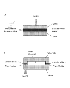
two solid supports. An example is shown in Panel A of Fig. 1, where a laser
beam
is directed orthogonal to the plane formed by the interface of the glass and
polyimide spacer. Scanning the laser from edge to edge along the plane will
produce
a linear bonding layer that runs from one edge to the other. By extrapolating
the
diagram in Panel A of Fig. 1 to a 3 dimensional configuration it will be
apparent that
the laser can be scanned in a raster pattern in the same plane (i.e. from edge
to edge
and also in and out of the page a distance d) to produce a bonding pattern
that runs
from edge to edge and has a width d. Turning to the flowcell layers shown in
Fig. 2
as an example, a laser can be scanned along the plane formed by the interface
of the
black polyimide and the glass to create a bonding layer. The path of the laser
can
correlate with the pattern of the black polyimide such that cutout regions
(that form
the channels) are avoided while other regions where black polyimide is in
contact
with the glass are irradiated. Although the method is exemplified with a laser
that
contacts the organic layer on the face that is in direct contact with the
layer of the
inorganic layer to which it will bond, it will be understood that irradiation
can occur
on the opposite side of the organic layer and heat can be transferred to the
bonding
face so long as a sufficiently thin organic layer is used.
An advantage of the laser bonding technique as that localized heating
produces a bonding layer without causing substantial deformation of the solid
supports. In contrast, other techniques that do not provide spatial
discrimination
when heating a spacer to the point of melting typically result in deformation
of the
spacer, which in turn deforms the shape of channels or other features in the
spacer.
To achieve bonding in the methods of the present disclosure, the irradiation
can pass through the inorganic solid support to contact the interface with the
organic
layer. As exemplified in Panel A of Fig. 1, the radiation from the laser
passes
through the upper glass support to contact the upper surface of the black
polyimide
spacer. The radiation beam is shown orthogonal to the plane of the interface
in the
figure, but in this or other embodiments the radiation beam can impinge at an
angle
with respect to the interface plane. Impinging at an angle can be beneficial
when
16
CA 02898453 2015-07-16
WO 2014/142841
PCT/US2013/030940
creating certain bonding patterns or to avoid features present on the
inorganic solid
support or on the organic solid support. Although not explicitly diagrammed in
the
static image shown in Panel A of Fig. 1, the lower glass support can be bonded
to
the black polyimide spacer by passing the laser beam through the lower glass
substrate to irradiate the interface between the black polyimide spacer and
the lower
glass support. Thus, both of the glass substrates can be bonded to opposite
surfaces
of the black polyimide layer to form the multilayer device.
An alternative configuration is shown in Panel B of Fig. 1. Here the organic
layer provides three sides to the channel (e.g. both the sidewalls and the top
for the
channel). In the diagram shown, the polyimide layer has laser bonding feet
that are
coated or locally impregnated with carbon black. Thus, the laser absorbing
layer is
present on the organic layer in a pattern that defines the channel footprint
on the
glass surface. In the example shown, the phenyl azide layer is also provided
in a
pattern that defines the footprint (optionally, the phenyl azide need not be
patterned).
Laser bonding of the components shown in Panel B of Fig. 1 will create a
multilayer
fluidic device having a single inorganic layer (e.g. glass) bonded to a single
organic
layer (e.g. polyimidc), wherein the organic layer is shaped to provide all but
one side
of the channel (i.e. the side formed by the glass surface).
As set forth above, a pattern of bonding between an inorganic solid support
and organic solid support can be created by selectively directing radiation in
a
pattern that delineates the bonding pattern. A pattern of bonding can also be
delineated by the surface pattern of the organic solid support, the pattern of
a
chemically reactive layer at the interface of the inorganic and organic
supports,
and/or the surface pattern of the inorganic support. Fig. 2 shows an example
where
the surface pattern of an organic support delineates the bonding pattern. In
this
example, the radiation pattern can replicate the pattern of the organic
support
surface. However, the radiation pattern need not follow the pattern of the
organic
support in this example since the cutouts in the organic solid support prevent
bonding at unwanted locations on the surface. This is also the case when using
a
pattern for the chemically reactive layer or a surface pattern for the
inorganic
support. Thus, a pattern of radiation can be optionally used in combination
with a
solid support surface pattern and/or a pattern of a chemically reactive layer.
17
CA 02898453 2015-07-16
WO 2014/142841
PCT/US2013/030940
The organic solid support need not be patterned prior to formation of a
bonding layer with an inorganic solid support. Rather, a pattern can be
created by
cutting the organic support after bonding has occurred. It is generally
advantageous
to use a selective radiation pattern, a pattern for the chemically reactive
layer and/or
a surface pattern for the inorganic support when the organic support is to be
cut after
bonding. Such patterning will allow for easier removal of the cut out area
since it
will not be attached to the inorganic support surface. Excess material can be
removed by cutting away with a laser tuned to a wavelength with significant
absorption in the spacer material, or with a blade-based cutter/plotter.
The present disclosure provides a fluidic device made, for example, by the
methods set forth above. For example, the present disclosure provides a
fluidic
device having at least one channel defined by an inorganic solid support
attached to
an organic solid support by a bonding layer, wherein the fluidic device is
made by
the process of: (a) contacting the inorganic solid support, the organic solid
support
and a radiation-absorbing material in a configuration wherein the radiation-
absorbing material is present at an interface between the inorganic solid
support and
the organic solid support; and (b) applying compression at the interface and
irradiating the radiation-absorbing material with the radiation to form the
bonding
layer between the inorganic solid support and the organic solid support. In
particular embodiments, the radiation-absorbing material is not an
electrically
conductive material such as a metal.
A fluidic device of the present disclosure, whether or not it is made by the
methods exemplified herein can include features and characteristics of the
multilayer
devices made by such methods. In particular embodiments, a fluidic device can
include (a) an inorganic solid support attached to an organic solid support by
a
bonding layer, wherein the inorganic solid support has a rigid structure and
wherein
the bonding layer includes a material that absorbs radiation at a wavelength
that is
transmitted by the inorganic solid support or the organic solid support, and
(b) at
least one channel formed by the attachment of the inorganic solid support to
the
organic solid support, wherein the channel is configured to contain a liquid
and the
bonding layer that attaches the inorganic solid support to the organic solid
support
provides a seal against liquid flow. In particular embodiments, the material
that
18
=
absorbs radiation is not an electrically conductive material. For example, in
some
embodiments, the material that absorbs radiation is not a metal.
A fluidic device of the present disclosure is particularly useful for array
analysis. For example, a fluidic device can contain an array having nucleic
acid
features. A particularly desirable use for the nucleic acid features is to
serve as
capture probes that hybridize to target nucleic acids having complementary
sequences. The target nucleic acids once hybridized to the capture probes can
be
detected, for example, via a label recruited to the capture probe. Methods for
detection of target nucleic acids via hybridization to capture probes are
known in the
art and include, for example, those described in US Pat. Nos.7,582,420;
6,890,741;
6,913,884 or 6,355,431 or US Pat. App. Pub. Nos. 2005/0053980 Al; 2009/0186349
Al or 2005/0181440 Al.
A nucleic acid array can also be used in a sequencing procedure, such as a
sequencing-by-synthesis (SBS) technique. Exemplary SBS procedures, fluidic
systems and detection platforms that can be readily adapted for use with an
array
produced by the methods of the present disclosure are described, for example,
in
Bentley et al., Nature 456:53-59 (2008), WO 04/018497; WO 91/06678; WO
07/123744; US Pat. Nos. 7,057,026; 7,329,492; 7,211,414; 7,315,019 or
7,405,281,
and US Pat. App. Pub. No. 2008/0108082 Al.
Other sequencing procedures that use cyclic reactions can be used,
such as pyrosequencing (Ronaghi, et al., Analytical Biochemistry 242(1),
84-9 (1996); Ronaghi, Genome Res. 11(1), 3-11 (2001); Rona& et al.
Science 281(5375), 363 (1998); US Pat. Nos. 6,210,891; 6,258,568 and
6,274,320), Sequencing-by-ligation (Shendure et al.
Science 309:1728-1732 (2005); US Pat. No. 5,599,675; and US Pat. No.
5,750,341),
sequencing-by-hybridization (Bains et al., Journal of Theoretical Biology
135(3),
303-7 (1988); Drmanac et al., Nature Biotechnology 16, 54-58 (1998); Fodor et
al., Science 251(4995), 767-773 (1995); and WO 1989/10977),
FRET-based sequencing (Levene et al. Science 299, 682-686 (2003); Lundquist et
al. Opt. Lett. 33, 1026-1028 (2008); Korlach et al. Proc. Natl. Acad. Sci. USA
105, 1176-1181(2008)), or sequencing based on detection of released protons
(US
Pat. App. Pub. Nos.
19
CA 2898453 2019-09-06
=
2009/0026082 Al; 2009/0127589 Al; 20 10/0 137 143 Al; or 20 10/02826 17 Al).
Other useful applications for an array of the present disclosure are gene
expression analysis or genotyping analysis. Exemplary methods for array-based
expression and genotyping analysis that can be carried out on an array of the
present
disclosure are described in US Pat. Nos.7,582,420; 6,890,741; 6,913,884 or
6,355,431 or US Pat. App. Pub. Nos. 2005/0053980 Al; 2009/0186349 Al or
2005/0181440 Al. Gene expression and genotyping can also be performed using
sequencing techniques.
The attachment of a nucleic acid to a feature can be via an intermediate
structure such as a bead, particle or gel. Attachment via a gel is exemplified
by
flowcells available commercially from Illumina Inc. (San Diego, CA) or
described in
WO 2008/093098. Exemplary gels that can be used in the methods and apparatus
set forth herein include, but are not limited to, those having a colloidal
structure,
such as agarose; polymer mesh structure, such as gelatin; or cross-linked
polymer
structure, such as polyacrylamide, SFATM (see, for example, US Pat. App. Pub.
No.
2011/0059865 Al) or PAZAMTm (see, for example, US Pat. App. Ser. No.
13/784,368). Attachment via a bead can be achieved as exemplified in the
description and cited references set forth previously herein.
In several embodiments, the surface of a fluidic device can include
oligonucleotide primers used for capture and/or amplification of template
nucleic
acids. The primers can be present as a lawn on one or more surfaces of the
device.
Alternatively, the primers can be present at patterned features as described,
for
example, in US Pat. App. Ser. Nos. 13/492,661; 13/661,524; 13/783,043; and
13/787,396. The primers can be universal primers that hybridize to a universal
adapter sequence that is attached to different target nucleic acids in a
library (i.e.
each target nucleic acid includes a target region that differs from other
target nucleic
acids in the library and several target nucleic acids in the library have the
same
universal adapter sequence). In some embodiments, a target nucleic acid can be
solid-support-attached, and primers (whether in solution or also solid-support-
attached) can be used to amplify the
CA 2898453 2019-09-06
=
attached target nucleic acid (i.e. the target nucleic acid can serve as a
template for
amplification).
A method set forth herein can use any of a variety of amplification
techniques. Exemplary techniques that can be used include, but are not limited
to,
polymerase chain reaction (PCR), rolling circle amplification (RCA), multiple
displacement amplification (MDA), or random prime amplification (RPA). In
particular embodiments, one or more primers used for amplification can be
solid-
support-attached. In PCR embodiments, one or both of the primers used for
amplification can be solid-support-attached. Formats that utilize two species
of
attached primer are often referred to as bridge amplification because double
stranded
amplicons form a bridge-like structure between the two attached primers that
flank
the template sequence that has been copied. Exemplary reagents and conditions
that
can be used for bridge amplification are described, for example, in U.S. Pat.
No.
5,641,658; U.S. Patent Publ. No. 2002/0055100; U.S. Pat. No. 7,115,400; U.S.
Patent Publ. No. 2004/0096853; U.S. Patent Publ. No. 2004/0002090; U.S. Patent
Publ. No. 2007/0128624; and U.S. Patent Publ. No. 2008/0009420. PCR
amplification can also be carried out with one of the amplification primers
being
solid-support-attached and the second primer being in solution. Exemplary
components that can be used in an RCA reaction and
principles by which RCA produces amplicons are described, for example, in
Lizardi
et al., Nat. Genet. 19:225-232 (1998) and US Pat. App. Pub. No. 2007/0099208
Al.
Some basic principles and useful conditions for MDA are described, for
example, in
Dean et al., Proc Natl. Acad. Sci. USA 99:5261-66 (2002); Lage et al., Genome
Research 13:294-307 (2003); Walker
et al., Molecular Methods for Virus Detection, Academic Press, Inc., 1995;
Walker
et al., Nucl. Acids Res. 20:1691-96 (1992); US Pat. Nos. 5,455,166; 5,130,238;
and 6,214,587.
The fbllowing examples are intended to illustrate but not limit the present
invention.
EXAMPLE I
Fabricating Flowcells
21
CA 2898453 2019-09-06
=
This example describes a method for fabricating a flowcell device by
bonding a polyimide spacer between two planar glass supports. A layer that
includes chemically reactive linkers and a radiation absorbing material is
formed
between the polyimide spacer and the glass. Laser activation of this layer
results in
bonding of the glass to the polyimide.
Diagrammatic representations of methods for fabricating a flowcell are
shown in Fig. 1 and Fig. 2. A rectangular glass slide is coated on one side
with (3-
aminopropy1)-triethoxysilane (APTES) to form an amino silane layer and the
amino
group is reacted with N-Hydroxysuccinimidy1-4-azidosalicylic Acid (HSAB) to
form a phenyl azide layer. A sheet of black KaptonTM (polymide containing
black
from DuPont) having rectangular dimensions similar to the glass slide and a
thickness of 100 microns is pre-patterned to contain cutouts for flowcell
lanes. A
spacer having cutouts for 6 lanes is exemplified in Fig. 2. The black KaptonTM
spacer is exposed to oxygen plasma and then compressed against the glass slide
with
approximately 100 PSI of pressure while laser energy at 1064 nm wavelength is
applied to the spacer. The laser spot can be scanned rapidly for higher power
lasers
(3500mmis for a 30W laser) or more slowly to accommodate lower power laser
systems (400mmis for a 6W laser). Continuous wave (CW) mode lasers have an
advantage of delivering even energy over time, but the process can be tuned to
use
pulse mode lasers as well.
The black KaptonTM spacer need not be pre-cut if the phenyl azide coating is
patterned on the glass slide (i.e. silane reagents are present at the
locations where
spacer will attach to form the walls of the channels and are absent from the
locations
where spacer material will be removed to form the channels). Alternatively or
additionally, the path of irradiation from the laser can follow the shape of
the spacer
such that bonding does not occur at the locations where spacer material will
be
subsequently cut out to form channels.
The resulting fluidic device will have several channels defined by the cutouts
in the spacer and the glass bottom support. These open channels can be
enclosed by
bonding a second glass slide, having similar rectangular dimensions as the
bottom
glass slide, to the exposed side of the black KaptonTM spacer. The top glass
slide is
coated with the phenyl azide layer, the spacer is exposed to oxygen plasma,
and the
top glass slide is compressed against the spacer while laser energy at 1064 nm
22
CA 2898453 2019-09-06
wavelength is applied to the black KaptonTM. One of the glass slides can be
pre-drilled
with ingress and egress apertures for the flowcell lanes (as exemplified in
Fig. 2).
Alternatively, the apertures can be drilled after bonding to the spacer.
As set forth above, a radiation absorbing material (e.g. carbon black) can be
present in the polyimide spacer to allow it to absorb the laser energy which
in turn
leads to formation of the bond between the glass and spacer. Alternatively, a
wavelength that is significantly absorbed by the natural polyimide material
(e.g. 480
nm) can be used instead of adding carbon black or other radiation absorbing
material
to the spacer. As another example, polyimide CEN JP can be bonded when
irradiated with light at 532 nm.
Without intending to be bound by theory, it is contemplated that the bond
formed using the methods of this example, may differ from a traditional
transmission laser weld where two materials melt and diffuse into one another
across
the interface. Rather, using the methods described in this example, the laser
energy
may be acting to soften one or both materials allowing for the contact
required for a
covalent bond to occur.
EXAMPLE II
Fabricating Flowcells for Use in Electric Field Assisted Nucleic Acid Capture
This example demonstrates a cost-effective, metal-free bonding technique
for flowcell assembly. An advantage of the technique is that metal, such as
titanium
which is often used to create a transmission laser weld, can be eliminated
from
flowcell fabrication. This can reduce the cost of materials for flowcell
manufacture
since titanium is relatively expensive. Avoiding metals such as titanium can
also
provide for a bond between the spacer and glass that is more robust for
applications
where an electrical current is passed through the flowcell; otherwise
electrochemistry can occur at the bonding interface to weaken the structure of
the
flowcell.
A diagrammatic representation of the bonding process is shown Fig. 3.
Borosilicate thin glass (D263 glass) having an indium tin oxide (ITO) coating
was
treated with plasma to activate the ITO surface and enrich it with hydroxyl
groups.
Next a vapor phase silanization was done with (3-aminopropy1)-trimethoxysilane
23
CA 2898453 2019-09-06
=
(APTMS) to covalently link surface ¨OH groups to the silane followed by a
thermal
bake step to completely crosslink the silane layer on the surface. The black
KaptonTM
(black polyimide) was then chemically bonded to the silanized surface using
1064
nm laser irradiation. Black polyimide absorbs strongly in the IR region of the
spectrum and it is a thermoplastic. Although not wishing to be bound by theory
it is
believed that the heated polyimide reflows at the silane interface to form
what
appear to be covalent bonds. As demonstrated in Example III, peel strengths
for the
resulting bond are comparable or surpass measured values achieved using
titanium
welded bonds for the same materials.
The bonding process at the whole flowcell level occurred similarly to that
shown in Fig. 2 (except that the surface coated glass included an ITO layer).
More
specifically, a black polyimide gasket was first UV laser cut with Cr/Au pads
evaporated directly on the black polyimide. To promote the adhesion of Cr/Au
to the
polyimide, an 02 plasma pre-treatment of the polyimide was performed. A Cr/Au
thickness of above 150 nm was beneficial to formation of robust, low
resistance
contacts upon bonding to the silanized ITO layer and allowed storage in
electrolyte
for over 1 week without measurable degradation of the conductance. This
technique
allows for good electrical contact to the ITO with contact resistance < 10
Ohms.
A photograph of a flowcell bonded using this technique is shown in Fig. 4.
The flowcell offers two electrical contacts per ITO layer. As diagrammed in
Fig. 5,
this allows for an input potential/waveform to be applied across a pair of
input
electrodes and the same potential/waveform can be measured across the output
electrodes ensuring minimal contact resistance.
To test the application of electric fields inside the flowcell, electric field
assisted patterning was performed as set forth in US Pat. App. Ser. No.
13/783,043,
with the following modifications. The electrodes were biased at 2V with K2SO4
filled in 4 of the flowcell lanes. A TET QC pre- and post E-field burnoff
revealed
that indeed oligonucleotide primers were removed (¨ 60% reduction in primer
intensity observed). Nucleic acid capture and
amplification was carried out on various lanes of the flowcell. Patterned
nucleic
acid clusters were clearly visible, confirming that electric fields could be
successfully applied in the flowcell using this technique.
24
CA 2898453 2019-09-06
To test the robustness of this flowcell bonding technique, 26 cycles of
sequencing were successfully completed on the flowcell without fluid leakage
or
vacuum failures. Sequencing was carried out as set forth in US Pat. App. Ser.
No.
13/783,043.
EXAMPLE III
Testing Structural Characteristics of Flowcells
This example describes methods for evaluating structural characteristics of
multilayer devices. This example also demonstrates advantageous features of
flowcells produced by the methods set forth in Example II.
Peel test
One way to measure the bond strength between the glass and polyimide is to
bond a test strip and then measure the force required to physically peel it
off the
glass. Typically a range of laser conditions are applied one per block down
the
length of a slide. The peel strip is then cut to a known width and length, and
can be
placed in the peel tester for measurement. The force applied to the grippers
is
measured approx 5 times a second to give a set of readings showing the peel
strength of each of the welded strips. Typically, the peel strip is cut into
two
sections, so that either both can be peeled under the same conditions (better
statistics) or one can be peeled after accelerated wet storage (to measure the
robustness of the bond to storage).
The peel test was used to compare the strength of the bond formed between
black KaptonTM and silanized glass in the presence or absence of laser
treatment. Black
KaptonTM films were uniformly treated as described in Example II and brought
into
contact with the glass under significant pressure (-100 PSI across the entire
film).
The glass was also treated as described in Example II. The laser was applied
to
selective areas of the two substrates (and not to other areas). Only those
areas which
were exposed to the laser formed a bonding layer. Non-lased areas remained
completely non-bonded, despite having identical chemistry and being compressed
together.
CA 2898453 2019-09-06
=
The peel test was also used to evaluate robustness of flowcells to storage in
aqueous solution. Pairs of flowcells were produced by the methods described in
Example II. Test flowcells were produced and stored in aqueous solution for 7
days
at 80 C prior to peel test. Control flowcells were produced and subjected to
peel
tests without prior storage in the aqueous solution. The results of the peel
tests
showed that storage did not adversely impact bonding strength for flowcells
produced by the methods set forth in Example II.
Pressure leak test
A flowcell was fabricated as described in Example II. Pressurized air/N2 (at
30PSI pressure) was then forced into all or some of the lanes through a
gasketed
pressure manifold. The rate at which the pressure decayed (due to air leaking
out)
was then monitored over 1 min. This is a non-destructive test, so the flowcell
can be
tested repeatedly over a succession of time points¨typically with the flowcell
being
held in accelerated storage conditions between the tests. In this way, the
quality of
the initial bond and how long the flowcell can be stored without developing
leaks
can be evaluated.
Flowcells were produced as described in Example II and stored in aqueous
solution at 80 C for various time periods prior to being subjected to the
pressure leak
test. The flowcells were shown to last 20-30 days in these conditions without
leaking
(>90% of tested flowcells passing).
The term "comprising" is intended herein to be open-ended, including not
only the recited elements, but further encompassing any additional elements.
Although the invention has been described with reference to the examples
provided above, it should be understood that various modifications can be made
without departing from the invention. Accordingly, the invention is limited
only by
the claims.
26
CA 2898453 2019-09-06