Note: Descriptions are shown in the official language in which they were submitted.
- 1 -
METHODS FOR MAKING A SUPERCONDUCTING DEVICE WITH AT LEAST
ONE ENCLOSURE
RELATED APPLICATIONS
This application claims priority under 35 U.S.C. 119(e) to U.S. application
number 61/754298, filed January 18, 2013, entitled, ERROR-CORRECTED QUANTUM
REGISTERS FOR A MODULAR SUPERCONDUCTING QUANTUM COMPUTER,
and U.S. application number 61/871061, filed August 28, 2013, entitled, ERROR-
CORRECTED QUANTUM REGISTERS FOR A MODULAR SUPERCONDUCTING
QUANTUM COMPUTER.
FEDERALLY SPONSORED RESEARCH
This invention was made with government support under Grant No. W911NF-09-
1-0514 awarded by United States Army ¨ Army Research Office. The US government
has
certain rights in the invention.
BACKGROUND
The present application relates generally to superconducting devices and
methods
of making superconducting devices. More specifically, the present application
relates to
superconducting devices formed from multiple substrates configured to exhibit
quantum
mechanical phenomena and methods for making such devices.
Quantum information processing uses quantum mechanical phenomena, such as
energy quantization, superposition, and entanglement, to encode and process
information
in a way not utilized by conventional information processing. For example, it
is known
that certain computational problems may be solved more efficiently using
quantum
computation rather than conventional classical computation. However, to become
a viable
computational option, quantum computation requires the ability to precisely
control a
large number of quantum bits, known as "qubits," and the interactions between
these
qubits. In particular, qubits should have long coherence times, be able to be
individually
manipulated, be able to interact with one or more other qubits to implement
multi-qubit
gates, be able to be initialized and measured efficiently, and be scalable to
large numbers
of qubits.
Date Recue/Date Received 2021-01-27
CA 02898608 2015-07-17
WO 2014/168665
PCT/US2014/012080
- 2 -
A qubit may be formed from any physical quantum mechanical system with at
least two orthogonal states. The two states of the system used to encode
information are
referred to as the "computational basis." For example, photon polarization,
electron spin,
and nuclear spin are two-level systems that may encode information and may
therefore be
used as a qubit for quantum information processing. Different physical
implementations
of qubits have different advantages and disadvantages. For example, photon
polarization
benefits from long coherence times and simple single qubit manipulation, but
suffers from
the inability to create simple multi-qubit gates.
Different types of superconducting qubits using Josephson junctions have been
proposed, including "phase qubits," where the computational basis is the
quantized energy
states of Cooper pairs in a Josephson Junction; "flux qubits," where the
computational
basis is the direction of circulating current flow in a superconducting loop:
and "charge
qubits," where the computational basis is the presence or absence of a Cooper
pair on a
superconducting island. Superconducting qubits are an advantageous choice of
qubit
because the coupling between two qubits is strong making two-qubit gates
relatively
simple to implement, and superconducting qubits are scalable because they are
mesoscopic components that may be formed using conventional electronic
circuitry
techniques.
SUMMARY
The inventors have recognized and appreciated that superconducting devices may
be manufactured using conventional microelectronic fabrication techniques.
Accordingly,
embodiments are directed to superconducting devices and methods for
manufacturing
superconducting devices.
Some embodiments are directed to a device including multiple substrates
comprising one or more troughs. The substrates are disposed such that the one
or more
troughs form at least one enclosure. At least one superconducting layer covers
at least a
portion of the at least one enclosure. In some embodiments, the plurality of
substrates
comprise a material with a crystalline structure, such as silicon.
In some embodiments, the at least one enclosure is configured to form at least
one
.. three-dimensional cavity resonator such that electromagnetic radiation at
one or more
frequencies resonates within the at least one three-dimensional cavity
resonator. The one
or more frequencies may include at least one microwave frequency. A Q factor
of the at
CA 02898608 2015-07-17
WO 2014/168665 PCT/US2014/012080
- 3 -
least one three-dimensional cavity resonator may be greater than ten million.
In some
embodiments, the at least one three-dimensional cavity resonator comprises a
first three-
dimensional cavity resonator and a second three-dimensional cavity resonator.
A Q factor
of the first three-dimensional cavity resonator may be greater than a Q factor
of the second
three-dimensional cavity resonator.
In some embodiments, at least one superconducting qubit is coupled to the at
least
one three-dimensional cavity resonator. The at least one superconducting qubit
may be a
transmon qubit or a fluxonium qubit. In some embodiments, a superconducting
wiring
layer is disposed on and/or in a first substrate of the plurality of
substrates. The
superconducting wiring layer may be configured to couple the at least one
superconducting qubit to the at least one three-dimensional cavity resonator.
In some
embodiments, at least one aperture in the at least one superconducting is
configured to
couple the superconducting wiring layer to the at least one three-dimensional
cavity
resonator. At least one via may connect the superconducting wiring layer to at
least one
superconducting component of a second substrate of the plurality of
substrates.
In some embodiments, the at least one superconducting qubit is disposed within
the
at least one three-dimensional cavity resonator such that the at least one
superconducting
qubit is configured to couple to the at least one three-dimensional cavity
resonator via
electromagnetic radiation.
In some embodiments, the plurality of substrates of the device include a first
substrate and a second substrate. The first substrate may include a first
trough of the one
or more troughs. The at least one superconducting layer may include a first
superconducting layer that covers at least a portion of the first trough; and
a second
superconducting layer that covers at least a portion of a surface of the
second substrate.
The first substrate and the second substrate may be disposed such that the
first
superconducting layer and the second superconducting layer are in direct
contact and the
first trough forms the at least one three-dimensional cavity resonator.
In some embodiments, the at least one enclosure is configured to form at least
one
electromagnetic shield such that external electromagnetic radiation is
prevented from
entering the at least one enclosure. At least one superconducting component
may be
disposed within the at least one electromagnetic shield. The at least one
superconducting
component may include at least one superconducting circuit, at least one qubit
and/or at
least on stripline resonator.
CA 02898608 2015-07-17
WO 2014/168665
PCT/US2014/012080
- 4 -
In some embodiments, the plurality of substrates comprises a first substrate
and a
second substrate. The first substrate may include a first trough of the one or
more troughs
and the second substrate may include a second trough of the one or more
troughs. The at
least one superconducting layer may include a first superconducting layer that
covers at
least a portion of the first trough and a second superconducting layer that
covers at least a
portion of the second trough. The first substrate and the second substrate may
be disposed
such that the first trough and the second trough form the at least one
enclosure. The at
least one stripline resonator may be disposed within the at least one
electromagnetic
shield. In some embodiments, at least one support layer suspended within the
at least one
electromagnetic shield, wherein the at least one stripline resonator is
disposed on and/or in
the at least one support layer. The at least one support layer may include at
least one
material selected from the group consisting of silicon, silicon oxide, and
silicon nitride. In
some embodiments, the at least one electromagnetic shield is configure to be a
part of a
circuit associated with the at least one stripline resonator.
In some embodiments, the one or more troughs comprises a first trough with a
first
trough surface opposed to a second trough surface, wherein the first trough
surface is not
parallel to the second trough surface. The at least one surface of the one or
more troughs
may be atomically smooth. The at least one enclosure may evacuated to a
pressure less
than atmospheric pressure.
Some embodiments are directed to a method for manufacturing a superconducting
device. The method includes acts of forming at least one trough in at least a
first
substrate; covering at least a portion of the first substrate with a
superconducting material;
covering at least a portion of a second substrate with the superconducting
material; and
bonding the first substrate and the second substrate to form at least one
enclosure
comprising the at least one trough and the superconducting material.
In some embodiments, the act of forming the at least one trough includes acts
of:
forming a mask layer that covers a portion of the first substrate; and etching
a portion of
the first substrate not covered by the mask layer. The act of etching may
include an act of
anisotropic etching using, for example, a wet etchant. The mask layer may
include silicon
nitride.
In some embodiments, the act of covering at least a portion of the first
substrate
with a superconducting material includes acts of: forming a seed layer on at
least the
portion of the first substrate; and electroplating the superconducting
material onto the seed
CA 02898608 2015-07-17
WO 2014/168665 PCT/US2014/012080
- 5 -
layer. The superconducting material may include one or more of aluminum,
niobium,
indium, rhenium, tantalum, titanium nitride, and niobium nitride.
In some embodiments, the method further includes acts of: forming channels in
at
least one wiring layer substrate; covering at least a portion of the channels
with the
superconducting material to form a wiring layer; and bonding the at least one
wiring
substrate to the first substrate and/or the second substrate. The act of
forming at least one
trough in at least a first substrate may include: forming a first trough in
the first substrate;
and forming a second trough in the second substrate, wherein the at least one
enclosure
comprises a first enclosure formed from the first trough and the second
trough. In some
embodiments, the at least one enclosure is configured to form at least one
electromagnetic
shield such that external electromagnetic radiation is prevented from entering
the at least
one enclosure. At least one superconducting component may be formed within the
first
enclosure. The at least one superconducting component may include at least one
superconducting circuit, at least one qubit and/or at least one stripline
resonator. In some
embodiments, at least a portion of said second substrate is covered with a
support layer
and at least one qubit is disposed on and/or within the support layer within
the cavity.
In some embodiments, the act of forming at least one trough in at least a
first
substrate further comprises forming a third trough in a third substrate, the
method further
comprising: covering at least a portion of the third substrate with the
superconducting
material; covering at least a portion of a fourth substrate with the
superconducting
material; bonding the third substrate and the fourth substrate to form a
memory layer
comprising a second enclosure from the third trough; and bonding the memory
layer to the
at least one wiring layer. The wiring layer may couple the second enclosure to
the first
enclosure. The first enclosure may be electrically connected to the wiring
layer through at
least one via. In some embodiments, a Q factor of the second enclosure is
greater than a Q
factor of the first enclosure.
In some embodiments, the method may also include coupling at least one qubit
to
the at least one enclosure. Coupling the at least one qubit to the at least
one enclosure may
include forming the at least one qubit within the at least one enclosure
and/or forming the
at least one qubit within the at least one enclosure. The at least one qubit
may be a
transmon qubit or a fluxonium qubit.
CA 02898608 2015-07-17
WO 2014/168665 PCT/US2014/012080
- 6 -
In some embodiments, the at least one enclosure is configured to form at least
one
three-dimensional cavity resonator such that electromagnetic radiation at one
or more
frequencies resonates within the at least one three-dimensional cavity
resonator.
BRIEF DESCRIPTION OF DRAWINGS
The accompanying drawings are not intended to be drawn to scale. In the
drawings, each identical or nearly identical component that is illustrated in
various figures
is represented by a like numeral. For purposes of clarity, not every component
may be
labeled in every drawing. In the drawings:
FIG. 1 illustrates a cross-sectional view of a superconducting device
comprising a
plurality of substrates and superconducting layers disposed to form a
plurality of
enclosures according to some embodiments;
FIG. 2 illustrates a cross-sectional view of a superconducting device
comprising a
three-dimensional cavity resonator enclosing a plurality of superconducting
qubits
disposed within the cavity according to some embodiments;
FIG. 3 illustrates a cross-sectional view of a superconducting device
comprising an
electromagnetic shield and a stripline resonator including a plurality of
qubits according to
some embodiments;
FIG. 4 illustrates a top view of a superconducting device comprising a
stripline
resonator comprising a plurality of superconducting qubits contained within an
electromagnetic shield according to some embodiments;
FIG. 5 illustrates a cross-sectional view of a plurality of acts of a method
for
constructing a superconducting device according to some embodiments;
FIG. 6 illustrates a cross-sectional view of forming a trough in a substrate
according to some embodiments;
FIG. 7is a flowchart of a method for constructing a superconducting device
according to some embodiments;
FIG. 8 is a flowchart of a method for forming a trough in a substrate
according to
some embodiments;
FIG. 9 is a method for constructing a superconducting device according to some
embodiments; and
FIG. 10 is a method for constructing a superconducting device according to
some
embodiments.
CA 02898608 2015-07-17
WO 2014/168665 PCT/US2014/012080
- 7 -
DETAILED DESCRIPTION
The inventors have recognized and appreciated that the coherence times of
superconducting devices can be significantly increased by using
microelectronic
fabrication techniques to form three-dimensional cavity resonators. These
devices are less-
sensitive to materials imperfections of both insulating substrates and
conductors than more
conventional, planar circuits. Significantly improved coherence times have
been observed
with three-dimensional resonators fabricated by conventional means. Such three-
dimensional resonators may also benefit, in some embodiments, from having
highly
smoothed surfaces with few imperfections. that can result from etching
techniques. In
.. some embodiments, a three-dimensional cavity resonator may be used as a
long-lived
memory for quantum information. A superconducting qubit may be coupled to the
three-
dimensional cavity resonator such that quantum information transferred from
the
superconducting qubit to the photonic energy states of the three-dimensional
cavity
resonator. In some embodiments, one or more superconducting qubits may be
coupled to
.. a three-dimensional cavity resonator through a wiring layer. In other
embodiments, one or
more superconducting qubits may be disposed within the three-dimensional
cavity
resonator such that electromagnetic radiation within the cavity couples
directly to the one
or more superconducting qubits.
The inventors have recognized and appreciated that an enclosure formed from a
superconducting material may shield components within the cavity from external
electromagnetic noise, and prevent decoherence by suppressing losses due to
electromagnetic radiation by the quantum circuit, even when the thickness of
the
superconducting material is small. Thus, superconducting layers may be formed
to cover
substrate layers to create precise, easily scaled superconducting devices. In
some
embodiments, an electromagnetic shield may enclose one or more superconducting
qubits
to shield the qubits from external noise, thereby increasing the performance
of the
superconducting qubits. For example, a stripline resonator comprising a
plurality of
superconducting qubits that act as a quantum bus may be disposed within an
electromagnetic shield enclosure. Moreover, thin superconducting shields
constructed
between the parts or subunits of a large quantum processor will improve
performance,
reliability, and ease of calibration of the quantum device. In some
embodiments, the
quantum bus may be coupled to one or more other superconducting components
such that
quantum information from a first component may be transferred to a second
component.
CA 02898608 2015-07-17
WO 2014/168665 PCT/US2014/012080
- 8 -
The inventors have also recognized and appreciated that using microelectronic
fabrication techniques to manufacture superconducting devices comprising at
least one
superconducting enclosure for use in quantum information processing allows
scalability
that is not available when cavities are formed from bulk material. In some
embodiments, a
plurality of enclosures and superconducting qubits may be formed in a single
device by
forming troughs in a plurality of substrates and bonding the substrates
together. In some
embodiments, one or more wiring layers may be used to connect components
together and
or connect components to external devices. In some embodiments, one or more
vias may
interconnect components and/or wiring layers that are in different substrate
layers. In this
way, a plurality of superconducting qubits and/or enclosures may be
interconnected in a
compact space.
Microelectronic fabrication techniques are processes used in the manufacture
of,
for example, micrometer sized structures for semiconductor devices and/or
microelectromechanical systems (MEMS). Examples of microelectronic fabrication
techniques include, but are not limited to: deposition techniques, such as
chemical vapor
deposition (CVD) and physical vapor deposition (PVD); photolithography;
etching
techniques, such as dry etching, wet etching, reactive ion etching (RIE),
isotropic etching
and anisotropic etching; chemical-mechanical planarization; ion implantation
techniques;
and thermal oxidation techniques.
Throughout the present application, the term "enclosure" is used to describe a
combination of superconducting layers that define a region of space that may
be empty
space or contain one or more superconducting devices of various types such as
wiring,
qubits, resonators, cavities, or other active devices within one or more
substrates. A
"three-dimensional cavity resonator" is a type of enclosure that is configured
to support
.. resonant electromagnetic radiation. An "electromagnetic shield" is a type
of enclosure
that is configured to prevent external electromagnetic radiation from entering
the
enclosure and prevent internal electromagnetic radiation from leaking out of
the enclosure
to the external environment.
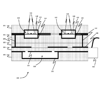
FIG. 1 illustrates a superconducting device 100 according to one embodiment.
The
superconducting device comprises a plurality of substrates 101-105 that are
bonded
together in any suitable way. For example, two substrates that have been
covered, at least
partially, with a metal material may be bonded together using cold welding,
thermocompression bonding, thermosonic bonding, eutectic bonding or solder
reflow. Any
CA 02898608 2015-07-17
WO 2014/168665 PCT/US2014/012080
- 9 -
suitable number of substrates may be bonded together to form superconducting
device
100. The embodiment illustrated in FIG. 1 shows five separate substrates 101-
105, but
embodiments are not so limited. For example, some embodiments may bond only
two
substrates together.
The different substrates of the superconducting device 100 may serve different
purposes. For example, substrate 101 and substrate 102 together form a bus
layer, which
is described in more detail in connection with FIGs. 3-4 below. Substrate 104
and
substrate 105 together form a cavity memory layer, which is described in more
detail
below in connection with FIG. 2. Substrate 103 is used as an interconnection
layer used to
interconnect various components within the superconducting device 100. The
interconnection layer comprises at least one wiring layer formed from a
superconducting
material disposed on and/or within the substrate 103 in a pattern that is
configured to
interconnect different components of the superconducting device 100.
The substrates 101-105 may comprise any suitable material. By way of example
and not limitation, the material may include any material with a crystalline
structure. For
example, silicon or germanium may be used. However, in some embodiments, the
substrate material may be insignificant as what controls the behavior of the
superconducting device is the superconducting material that coats various
portions of the
substrate and the troughs that are created within the substrate to form
enclosures.
Additionally, the substrates 101-105 may be of any suitable dimensions. By way
of
example and not limitation, the substrates 101-105 may have a thickness
ranging from 300
ium to 500 rim.
The superconducting layers of the superconducting device 100 may be formed in
any suitable way. In some embodiments, the surface of the substrate is covered
with a
.. superconducting material. In other embodiments, one or more channels and/or
troughs
may be formed in the substrate that are subsequently covered, at least in
part, with a
superconducting material. Any suitable thickness of superconducting layer may
be used.
In some embodiments, a superconducting layer of superconducting device 100 may
have a
thickness ranging from 1 ium to 10 ium. Additionally, any suitable
superconducting
material may be used. By way of example and not limitation, the
superconducting
material may include aluminum, niobium, indium, rhenium, tantalum, titanium
nitride,
and/or niobium nitride.
CA 02898608 2015-07-17
WO 2014/168665 PCT/US2014/012080
- 10 -
In some embodiments, superconducting device 100 may communicate to external
components via a planar-to-coaxial transition component 150 or any other
suitable
electronic connection, as known is in the art.
FIG. 1 illustrates a single cross-section of the device showing three separate
enclosures 110, 120 and 130. One of skill in the art would recognize that
other cross-
sections at different positions into and out of the plane of the figure may
include additional
enclosures that may be coupled to the enclosures 110, 120 and 130 through the
wiring
layer 140, the vias 142 and 144, and/or additional wiring layers and vias not
illustrated.
Additionally, the wiring on a given layer or vias between layers may be
separately
enclosed by additional superconducting layers (not shown) realized by the
same, or
different, methods. The idea that all electromagnetic signals should be
carried on properly
designed transmission line structures, such as striplines or coaxial lines,
and that these may
be realized by the embodiment of our method for realizing superconducting
enclosures,
should be clear to one skilled in the art.
As mentioned above, a cavity memory layer may be formed from substrate 104
and 105. A trough is formed in the substrate 105 and covered, at least in
part, with a
superconducting layer 132. At least a portion of substrate 104 is also covered
in a
superconducting layer 134. The trough may be any suitable shape or size. For
example,
the trough may extend from a surface of the substrate by about 300 p m. The
substrates are
then positioned such that when connected together, a three-dimensional cavity
resonator
130 is formed. FIG. 2 illustrates an embodiment 200 of a cavity memory layer
in more
detail. The three-dimensional cavity resonator130 includes at least a first
surface 232 and
a second surface 234 that are opposed to one another. In some embodiments, the
two
surfaces are parallel to one other. In other embodiments, the first surface
232 and the
second surface 234 may both form a non-perpendicular angle with the
superconducting
layer 134 associated with substrate 104. In some embodiments, every surface of
the three-
dimensional cavity resonator 130 is covered, at least in part, with a
superconducting
material. In some embodiments, each surface of the three-dimensional cavity is
covered in
its entirety except for two apertures 236 and 238 formed in the
superconducting layer 134.
The apertures 236 and 238 may be used to couple electromagnetic radiation into
the three-
dimensional cavity resonator 130 from the wiring layer 140. Other methods of
coupling to
the cavity, which would be known by those skilled in the art, may also be
employed.
CA 02898608 2015-07-17
WO 2014/168665
PCT/US2014/012080
- 11 -
The geometry of the three-dimensional cavity resonator 130 determines which
frequencies of electromagnetic radiation will be resonant with the cavity. In
some
embodiments, the three-dimensional cavity resonator 130 may be configured to
resonate at
microwave frequencies. By way of example and not limitation, the three-
dimensional
.. cavity resonator 130 may be configured to resonate at at least one
frequency ranging
between 1 GHz and 20 GHz. As a further example, the three-dimensional cavity
130 may
be configured to resonate at at least one frequency ranging between 5 GHz and
9 GHz.
In some embodiments, the superconducting device 200 may include one or more
superconducting qubits 131 disposed within the three-dimensional cavity
resonator 130.
Any suitable superconducting qubit may be used. By way of example and not
limitation,
each of the superconducting qubits 131 may be a transmon qubit or a fluxonium
qubit.
Each of the superconducting qubits 131 may comprise a Josephson junction
disposed
between two superconducting portions that act as a dipole antenna. In some
embodiments
the superconducting qubits 131 are oriented vertically such that the axis of
each
superconducting qubit (as determined by the orientation of the dipole antenna)
is
perpendicular to the superconducting layer 134 used to form the apertures 236
and 238,
and the qubits thereby couple to the electromagnetic fields of the resonant
cavity.
In other embodiments, the three-dimensional cavity resonator 130 does not
contain
a superconducting qubit, but is instead coupled to a superconducting qubit
through wiring
layer 140. In this way, an external superconducting qubit (not shown) may
transfer
quantum information to the three-dimensional cavity resonator 130, which may
act as a
memory for the quantum information.
Quantum information may be stored in the three-dimensional cavity resonator
130in any suitable way. For example, the energy eigenstates of the
electromagnetic field
may be used as the computational basis for encoding quantum information.
Alternatively,
different coherent states and/or superpositions of coherent state (sometimes
called "cat
states") may be used as the computational basis. Embodiments are not limited
to any
particular technique for encoding the quantum information in the three-
dimensional cavity
resonator 130.
As mentioned above, substrate 101 and substrate 102 of FIG. 1 form a bus
layer.
The bus layer includes enclosure 110 and enclosure 120, which are configured
to be
electromagnetic shields. Electromagnetic shield 110 includes a plurality of
qubits 116
formed on and/or in a support layer 118 that is suspended within the
electromagnetic
CA 02898608 2015-07-17
WO 2014/168665 PCT/US2014/012080
- 12 -
shield 110. Electromagnetic shield 110 includes a superconducting layer 112
and a
superconducting layer 114 for enclosing the qubits 116, thereby shielding the
qubits 116
from external electromagnetic noise and preventing unwanted electromagnetic
radiation
from entering the enclosure. The electromagnetic shield 110 also prevents
electromagnetic radiation from within the enclosure from leaking to the
external
environment. Similarly, electromagnetic shield 120 includes a plurality of
qubits 126
formed on and/or in a support layer 128 that is suspended within the cavity
120.
Electromagnetic shield 120 includes a superconducting layer 122 and a
superconducting
layer 124 for enclosing the qubits 126, thereby shielding the qubits 126 from
external
electromagnetic noise and preventing unwanted electromagnetic radiation or
cross-
coupling to other elements of the device.
FIG. 3 illustrates a more detailed cross-sectional view 300 of electromagnetic
shield 110 according to some embodiments. Substrate 102 includes a trough from
which
the electromagnetic shield 110 is formed. At least a portion of the trough is
covered with
a superconducting layer 114. The superconducting layer 114 may also cover
portions of
the substrate 102 that are part of the trough. A plurality of qubits 116 are
formed in and/or
on a support layer 118. In some embodiments, the support layer is a dielectric
membrane
suspended across the trough in substrate 102. Any suitable material may be
used to form
the support layer. By way of example and not limitation, the support layer may
comprise
silicon, silicon oxide, or silicon nitride. The plurality of qubits 116 may be
any suitable
superconducting qubit, such as a transmon qubit or a fluxonium qubit. Each
individual
qubit of the plurality of qubits 116 may be individually controlled and/or
detected using
feed lines 312, which are formed in and/or on the support layer 118. A
stripline resonator
310 is disposed between a first plurality of qubits and a second plurality of
qubits. In
some embodiments, the stripline resonator 310 may be approximately 20 ium
wide. The
feed lines 312 and the stripline resonator 310 may be formed from any suitable
superconducting material.
Substrate 101 also includes a trough that has approximately the same
dimensions
and the trough in substrate 102. At least a portion of the trough in substrate
101 is covered
with a superconducting layer 112. Substrate 101 is disposed near substrate 102
such that a
gap exists between feedline 312 and superconducting layer 112. In some
embodiments,
the gap may be approximately 10 p.m. Substrate 101 and substrate 102 may be in
contact
with each other at a location away from electromagnetic shield 110 such that
they may be
CA 02898608 2015-07-17
WO 2014/168665
PCT/US2014/012080
- 13 -
bonded together. By enclosing the stripline resonator 310 and the plurality of
qubits 116
in an electromagnetic shield, the enclosed components are isolated from
external
electromagnetic noise, and decoherence due to unwanted electromagnetic
radiation and
cross-couplings are prevented.
FIG. 4 illustrates a top view 400 of the support layer 118 and the components
included thereon. The arrows indicating "A" illustrate a plane representing
the location of
the cross-section view 300 of FIG. 3. Membrane 118 includes a plurality of
superconducting qubits 116. In some embodiments, each superconducting qubit is
a
superconducting qubit, such as a transmon qubit or a fluxonium qubit. FIG. 4
illustrates
transmon qubits 116 comprising a Josephson junction 412 between a first
superconducting
portion 414 and a second superconducting portion 416. Each qubit 116 may be
individually controlled and/or read-out using drive feed lines 314. A large
portion of the
surface of the support layer 118 is covered with a superconducting layer as
the ground
plane for the stripline resonator 430. The stripline resonator 430 is driven
via feedlines
420. There is a gap between the feedlines 420 and the stripline resonator such
that the two
components are weakly, capacitively coupled. Optionally, there are a plurality
of holes
410 in the support layer 118 to reduce the amount of dielectric present in the
enclosure in
which the support layer is disposed and increase the amount of vacuum present
in the
enclosure, which may increase performance.
Superconducting devices according to certain embodiments may be manufactured
in any suitable way. For example, microelectronic fabrication techniques may
be used.
Alternatively, the substrates may be formed with troughs and channels as
desired using
three-dimensional printing techniques and the superconducting layers may be
formed
using, for example, electroplating techniques. Some embodiments may create
enclosures
by forming a trough in a single substrate, as illustrate in FIG. 2.
Alternatively, or in
addition, enclosures may be created by forming a first trough in a first
substrate and a
second trough in a second substrate and placing the two substrates together
with the two
troughs adjacent to one another. Methods for forming superconducting devices
according
to some embodiments are described below with reference to FIGs. 5-10.
FIG. 5 illustrates a cross-sectional view of a plurality of acts of a method
for
constructing a superconducting device according to some embodiments. A
flowchart of
the acts of the method 700 according to some embodiments is shown in FIG. 7.
At act
702, a first trough is formed in a first substrate. The trough may be formed
in any suitable
CA 02898608 2015-07-17
WO 2014/168665
PCT/US2014/012080
- 14 -
way. In some embodiments, the substrate and trough may be printed using three-
dimensional printing techniques. In other embodiments, microelectronic
fabrication
techniques may be used. Details of one such embodiment is now described in
connection
with FIG. 5. FIG. 6 and FIG. 8.
FIG. 5A illustrates a first substrate 500 being provided. Any suitable
substrate
may be used. In some embodiments, the substrate may be formed from a material
with a
crystalline structure. For example, the substrate may comprise silicon or
germanium. The
substrate 500 may be of any suitable thickness. In the illustrated
embodiments, the
substrate is approximately 500 p m thick.
At act 802, a silicon nitride layer 502 is deposited on a first surface of the
substrate
500 (see FIG. 5B). While silicon nitride is used in the illustrative
embodiment of FIG. 5,
any suitable material that may act as a mask may be used.
At act 804, a photoresist layer 504 is deposited on top of the silicon nitride
layer
502 (see FIG. 5C). The photoresist layer 504 is formed in a pattern based on
the
dimensions of the trough being formed in the substrate 500. Accordingly, the
photoresist
layer is absent from the region above where the trough will be formed in the
substrate in
the subsequent acts. By way of example and not limitation, the photoresist
layer 504 may
be formed such that an area of the silicon nitride layer 502 with dimensions
18 mm by 38
mm is left exposed.
At act 806, the exposed portion of the silicon nitride layer 502 is removed
(see
FIG. 5D). This may be achieved in any suitable way. In some embodiments, the
silicon
nitride layer 502 is etched using an etchant that removes the silicon nitride
layer, but does
not remove the photoresist. For example, reactive ion etching (RIE) may be
used to etch
the silicon nitride layer. The act of RIE may use, for example, CHF3/02 as an
etchant.
The photoresist layer 504 is then removed at act 808. The resulting structure
is the
substrate 500 partially covered with the silicon nitride layer 502 which will
act as a mask
for defining dimensions of the trough (see FIG. 5E).
At act 810, the exposed portion of the substrate 500 is etched to form a
trough 506.
Any suitable etching may be performed. In some embodiments, the substrate 500
may be
etched such that opposing surfaces of the resulting trough 506 are parallel to
one another.
In the embodiment shown in FIG. 5F, the trough is etched using an anisotropic
wet etch
using 30% KOH at 85 C. The details of the anisotropic etch is shown in more
detail in
FIG. 6.
CA 02898608 2015-07-17
WO 2014/168665
PCT/US2014/012080
- 15 -
FIG. 6 illustrates the trough 506 resulting from an anisotropic wet etch.
Because
of the crystalline structure of the silicon substrate 500, the (100) plane 612
and the (111)
614 plane for a 54.7 angle as a result of the etching act. In some
embodiments, the
anisotropic wet etch results in surfaces 612 and 614 that are atomically
smooth. Thus,
when covered in a superconducting layer the surface of the resulting enclosure
will be
substantially free from defects. If the enclosure is configured for use as a
three-
dimensional cavity resonator, the smooth surfaces result in a high Q factor
cavity.
At act 812, the silicon nitride layer is removed resulting in the substrate
500
including the trough 506 (see FIG. 5G). While FIG. 8 illustrated one
embodiment of a
method for creating a trough in a substrate, any suitable method may be used.
For
example, laser machining or three-dimensional printing may be used to form a
substrate
with a trough.
Returning to FIG. 7, after the trough is formed in a substrate at act 702 the
method
700 continues at act 704, where at least a portion of the first substrate is
covered with a
superconducting material. In some embodiments, all the surfaces of the trough
in the
substrate may be covered. In other embodiments, only portions of the surfaces
may be
covered. In this way, for example, apertures may be formed. In some
embodiments,
portions of the substrate outside of the region associated with the trough may
also be
covered with a superconducting layer.
The superconducting layer may be formed in any suitable way. For example,
FIGs. 5H-I illustrate one particular method for forming a superconducting
layer that
covers at least a portion of the substrate. FIG. 5H illustrates a thin seed
layer 508 is
deposited over the surface of the substrate 500. This may be done in any
suitable way. In
some embodiments, copper is deposited via evaporation techniques to form the
seed layer
508. Any suitable thickness of seed layer may be used. For example, the seed
layer 508
may be approximately 200 nm thick. While copper is used as an example material
for the
seed layer 508, any suitable material may be used.
FIG. 5I illustrates a superconducting layer 510 formed on the seed layer 508.
This
may be done in any suitable way. For example, a superconducting material may
be
electroplated onto the seed layer. The superconducting layer 510 may be formed
with any
suitable thickness. For example, the superconducting layer 510 may be
approximately
101.1m thick. Any suitable superconducting material may be used. For example,
the
- 16 -
superconducting layer may comprise aluminum, niobium, indium, rhenium,
tantalum,
titanium nitride, or niobium nitride.
At act 706, a second trough is formed in a second substrate. The act of
forming the
second trough may be achieved using the same techniques described in
connection with
.. act 702, FIG. 5 and FIG. 8. However, the formation of the second trough is
optional. An
enclosure may be formed from a single trough in a first substrate without
forming a second
trough in a second substrate.
At act 708, at least a portion of the second substrate is covered with a
superconducting material. This act may be achieved using the techniques
described in
connection with act 704. In embodiments where a second trough is formed in the
second
substrate, at least a portion of every surface of the trough may be covered
with a
superconducting layer. In some embodiments, a portion of the second substrate
outside of
the trough region may be at least partially covered with a superconducting
layer.
At act 710, at least one superconducting qubit is formed on a support layer.
In
some embodiments, the support layer may be any suitable dielectric membrane.
For
example, the support layer may comprise silicon, silicon oxide, or silicon
nitride. In some
embodiments, act 710 may be omitted as superconducting devices may be formed
without
a superconducting qubit being enclosed in an enclosure.
At act 712, the first substrate and the second substrate are bonded together
to form
an enclosure. In embodiments where the first trough was formed in the first
substrate and
a second trough was formed in the second substrate, the two troughs are
positioned
adjacent to one another such that the enclosure is formed from both troughs
together as shown
in FIG. 5J. In some embodiments where at least one superconducting qubit is to
be enclosed by an
enclosure, the support layer is suspended across the first trough prior to
bonding the two
.. substrates together. Accordingly, the at least one qubit in and/or on the
support layer is
disposed within the enclosure.
The method 700 may also include additional optional acts shown in FIG. 9 and
FIG. 10. For example, the result of performing method 700 may be the formation
of
enclosure 110 in the bus layer of FIG. I. FIG. 9 illustrates additional acts
for forming the
wiring layer 140 and the memory layer enclosure 130. FIG. 10 illustrates
additional acts
for forming the second enclosure 120 in the bus layer.
FIG. 9 illustrates additional acts 900 for forming the wiring layer and the
memory
layer. In some embodiments, the additional acts may be performed after the
method 700.
Date Recue/Date Received 2021-01-27
CA 02898608 2015-07-17
WO 2014/168665
PCT/US2014/012080
- 17 -
In other embodiments, the additional acts may be performed before the method
700 or
simultaneously with method 700.
At act 902, at least one channel is formed in wiring layer substrate 103 (see
FIG. 1). The at least one channel may be formed, for example, using the same
process
used to create the trough in act 702.
At act 904, at least a portion of the at least one channel is covered with
superconducting material. This may be achieved using the same process used
above in
connection with act 704. In some embodiments, the channel may be completely
filled
with superconducting material. In other embodiments, the one or more of the
surfaces of
the at least one channel may be covered with the superconducting material.
At act 906, the wiring substrate 103 is bonded to substrate 102. The
substrates
may be bonded in any suitable way, as discussed above.
At act 908, a trough is formed in substrate 105 using, for example, the same
process used to create the trough in act 702.
At act 910, at least a portion of substrate 105 is covered with a
superconducting
material. This may be achieved using the same process used above in connection
with act
704. In some embodiments, each surface of the through is completely covered
with
superconducting material. The superconducting material is formed in a layer
that may be
any suitable thickness. In some embodiments, the superconducting layer may be
approximately 1 0m thick. In other embodiments, the superconducting layer may
be
approximately 10 ium thick.
At act 912, at least a portion of substrate 104 is covered with a
superconducting
material. This may be achieved using the same process used above in connection
with act
704. Certain portions of a surface of substrate 104 may be left exposed. For
example, the
area corresponding to apertures 236 and 238 in FIG. 2 may not be covered with
superconducting material.
At act 914, substrate 104 is bonded to substrate 105 such that the trough
forms a
three-dimensional cavity resonator. The substrates may be bonded in any
suitable way, as
discussed above.
At act 916, the memory layer is bonded to the wiring layer. The substrates
associated with the layers may be bonded in any suitable way, as discussed
above.
FIG. 10 illustrates additional acts for forming the second enclosure 120 in
the bus
layer.
CA 02898608 2015-07-17
WO 2014/168665 PCT/US2014/012080
- 18 -
At act 1002, a trough associated with enclosure 120 is formed in the substrate
101
using, for example, the same process used to create the trough in act 702. In
some
embodiments, the trough associate with enclosure 120 may be formed
simultaneously with
the trough associated with enclosure 110.
At act 1004, a trough associated with enclosure 120 is formed in the substrate
102
using, for example, the same process used to create the trough in act 702. In
some
embodiments, the trough associate with enclosure 120 may be formed
simultaneously with
the trough associated with enclosure 110.
At act 1006, at least a portion of substrate 102 may be covered with a support
layer
which is suspended over the trough associated with enclosure 120. This support
layer may
be fon-ned in the same way as the support layer associated with enclosure 110.
At act 1008, at least one qubit is formed on the support layer. This at least
one
qubit may be formed in the same way as the support layer associated with
enclosure 110.
Having thus described several aspects of at least one embodiment of a
superconducting device and at least one method for manufacturing a
superconducting
device, it is to be appreciated that various alterations, modifications, and
improvements
will readily occur to those skilled in the art. For example, superconducting
enclosures of
any size may be included. Some enclosures may have dimensions on the order of
a
centimeter, a millimeter, or a micrometer. Such alterations, modifications,
and
improvements are intended to be part of this disclosure, and are intended to
be within the
spirit and scope of the invention. While the present teachings have been
described in
conjunction with various embodiments and examples, it is not intended that the
present
teachings be limited to such embodiments or examples. On the contrary, the
present
teachings encompass various alternatives, modifications, and equivalents, as
will be
appreciated by those of skill in the art.
While various inventive embodiments have been described and illustrated, those
of
ordinary skill in the art will readily envision a variety of other means
and/or structures for
performing the function and/or obtaining the results and/or one or more of the
advantages
described, and each of such variations and/or modifications is deemed to be
within the
.. scope of the inventive embodiments described. More generally, those skilled
in the art
will readily appreciate that all parameters, dimensions, materials, and
configurations
described are meant to be exemplary and that the actual parameters,
dimensions, materials,
and/or configurations will depend upon the specific application or
applications for which
- 19 -
the inventive teachings is/are used. Those skilled in the art will recognize,
or be able to
ascertain using no more than routine experimentation, many equivalents to the
specific
inventive embodiments described. It is, therefore, to be understood that the
foregoing
embodiments are presented by way of example only and that, within the scope of
the
appended claims and equivalents thereto, inventive embodiments may be
practiced
otherwise than as specifically described and claimed. Inventive embodiments of
the
present disclosure may be directed to each individual feature, system, system
upgrade,
and/or method described. In addition, any combination of two or more such
features,
systems, and/or methods, if such features, systems, system upgrade, and/or
methods are
not mutually inconsistent, is included within the inventive scope of the
present disclosure.
Further, though some advantages of the described embodiments may be indicated,
it should be appreciated that not every embodiment will include every
described
advantage. Some embodiments may not implement any features described as
advantageous. Accordingly, the foregoing description and drawings are by way
of
example only.
The section headings used are for organizational purposes only and are not to
be
construed as limiting the subject matter described in any way.
Also, the technology described may be embodied as a method, of which at least
one example has been provided. The acts performed as part of the method may be
ordered
in any suitable way. Accordingly, embodiments may be constructed in which acts
are
performed in an order different than illustrated, which may include performing
some acts
simultaneously, even though shown as sequential acts in illustrative
embodiments. In
addition, certain acts performed as part of the method may be optional.
Accordingly,
embodiments may be constructed in which certain acts are not performed at all.
All definitions, as defined and used, should be understood to control over
dictionary definitions, and/or ordinary meanings of the defined terms.
The terms "about," "approximately." and "substantially" may be used to refer
to a
value, and are intended to encompass the referenced value plus and minus
acceptable
variations. The amount of variation could be less than 5% in some embodiments.
less than
10% in some embodiments, and yet less than 20% in some embodiments. In
embodiments
where an apparatus may function properly over a large range of values, e.g., a
range
including one or more orders of magnitude, the amount of variation could be a
factor of
Date Recue/Date Received 2021-01-27
CA 02898608 2015-07-17
WO 2014/168665 PCT/US2014/012080
- 20 -
two. For example, if an apparatus functions properly for a value ranging from
20 to 350,
"approximately 80" may encompass values between 40 and 160.
The indefinite articles "a" and "an," as used in the specification and in the
claims,
unless clearly indicated to the contrary, should be understood to mean "at
least one."
The phrase "and/or," as used in the specification and in the claims, should be
understood to mean -either or both" of the elements so conjoined, i.e.,
elements that are
conjunctively present in some cases and disjunctively present in other cases.
Multiple
elements listed with -and/or" should be construed in the same fashion, i.e., -
one or more"
of the elements so conjoined. Other elements may optionally be present other
than the
elements specifically identified by the "and/or" clause, whether related or
unrelated to
those elements specifically identified. Thus, as a non-limiting example, a
reference to "A
and/or B", when used in conjunction with open-ended language such as
"comprising" can
refer, in one embodiment, to A only (optionally including elements other than
B); in
another embodiment, to B only (optionally including elements other than A); in
yet
another embodiment, to both A and B (optionally including other elements);
etc.
As used in the specification and in the claims, "or" should be understood to
have
the same meaning as "and/or" as defined above. For example, when separating
items in a
list, "or" or "and/or" shall be interpreted as being inclusive, i.e., the
inclusion of at least
one, but also including more than one, of a number or list of elements, and,
optionally,
additional unlisted items. Only terms clearly indicated to the contrary, such
as "only one
of' or -exactly one of." or, when used in the claims, "consisting of," will
refer to the
inclusion of exactly one element of a number or list of elements. In general,
the term -or"
as used shall only be interpreted as indicating exclusive alternatives (i.e.
"one or the other
but not both") when preceded by terms of exclusivity, such as "either," "one
of," "only
one of," or "exactly one of." "Consisting essentially of," when used in the
claims, shall
have its ordinary meaning as used in the field of patent law.
As used in the specification and in the claims, the phrase "at least one," in
reference to a list of one or more elements, should be understood to mean at
least one
element selected from any one or more of the elements in the list of elements,
but not
necessarily including at least one of each and every element specifically
listed within the
list of elements and not excluding any combinations of elements in the list of
elements.
This definition also allows that elements may optionally be present other than
the elements
specifically identified within the list of elements to which the phrase "at
least one" refers,
CA 02898608 2015-07-17
WO 2014/168665 PCT/US2014/012080
- 21 -
whether related or unrelated to those elements specifically identified. Thus,
as a non-
limiting example, "at least one of A and B" (or, equivalently, "at least one
of A or B," or,
equivalently "at least one of A and/or B") can refer, in one embodiment, to at
least one,
optionally including more than one, A. with no B present (and optionally
including
elements other than B); in another embodiment, to at least one, optionally
including more
than one, B, with no A present (and optionally including elements other than
A); in yet
another embodiment, to at least one, optionally including more than one, A,
and at least
one, optionally including more than one, B (and optionally including other
elements); etc.
In the claims, as well as in the specification above, all transitional phrases
such as
"compri sing," "including," "carrying," "having," "containing," "involving,"
"holding,"
"composed of," and the like are to be understood to be open-ended, i.e., to
mean including
but not limited to. Only the transitional phrases "consisting of' and
"consisting essentially
of' shall be closed or semi-closed transitional phrases, respectively.
The claims should not be read as limited to the described order or elements
unless
stated to that effect. It should be understood that various changes in form
and detail may
be made by one of ordinary skill in the art without departing from the spirit
and scope of
the appended claims. All embodiments that come within the spirit and scope of
the
following claims and equivalents thereto are claimed.
Use of ordinal terms such as "first", "second", "third", etc., in the claims
to modify
a claim element does not by itself connote any priority, precedence, or order
of one claim
element over another or the temporal order in which acts of a method are
performed, but
are used merely as labels to distinguish one claim element having a certain
name from
another element having a same name (but for use of the ordinal term) to
distinguish the
claim elements.
What is claimed is: