Note: Descriptions are shown in the official language in which they were submitted.
CA 02898763 2015-07-21
WO 2014/110683
PCT/CA2014/050040
DIELECTRIC GEOMETRY FOR
CAPACITIVE-BASED TACTILE SENSOR
CROSS-REFERENCE TO RELATED APPLICATION
[0001] The present application claims priority on United States
Provisional Patent
Application Serial No. 61/754,758, filed on January 21, 2013.
TECHNICAL FIELD
[0002] The present disclosure relates to capacitive-based tactile sensors
and to
dielectrics used therein.
BACKGROUND OF THE ART
[0003] Some known capacitive-based tactile sensors use the relative
change in
distance d between two conductive plates as a way to measure the applied
pressure pa, namely:
A
paocC r
= 0 - ( 1 )
d
[0004] where C is the capacitance value, Sr and so are respectively the
relative
static permittivity and the vacuum permittivity and A is the overlap area of
the
plates. One element that often limits the sensitivity of these sensors is the
mechanical response of the non-conductive material used between the electrodes
and the ground plane, that serves as a dielectric as well as a spring-like
element. It
has been known to use a plain layer of soft polymer such as silicone [1] to
create a
soft dielectric (i.e., a non-rigid or resilient) that will deform under
applied stress.
[0005] However, silicone and many other polymers used for such purpose
may
be considered as being incompressible. Hence, for a wide range of applied
pressure, their volume will remain unchanged. In reaction to a compressive
force on
a specific area, some region of the dielectric will have to expand. This
behavior may
lead to inadequate compliance of the soft material as well as a relatively
slow
recovery time once pressure is released, two shortcomings that may result in
hysteresis and in a relatively low sensor sensitivity.
1
CA 02898763 2015-07-21
WO 2014/110683
PCT/CA2014/050040
[0006] To circumvent these drawbacks, silicone foam [2] or urethane foam
[3]
have been used as a dielectric for capacitive-based tactile sensor. Although,
the
volume of a foam under pressure can change, thus leading to a pressure sensor
with increased sensitivity, regular foam is also subject to hysteresis. Ulmen
et al. [4]
have thus suggested using a closed cell polyurethane foam. The ratio of
stiffness to
damping in a foam with a closed cell structure is higher due to the trapped
air that
acts as spring-like elements. The nonlinearity of the response may thus be
reduced.
However, because of this structure, the stiffness of these foams is typically
relatively
high and their permittivity relatively low, thus leading to an average
sensitivity. In
order to increase the sensitivity and decrease the hysteresis, Mannsfeld et al
[5]
made a significant breakthrough by creating a microstuctured dielectric made
out of
polydimethylsiloxane (PDMS). By creating microfeatures in a PDMS layer using
soft
lithography, a material has been created with room for silicone to expand
locally.
Consequently, the apparent stiffness of the dielectric has been lowered and
hysteresis has been reduced. However, the manufacturing of such a sensor, due
to
the size of the features, is based on soft lithography. Soft lithography is a
time-
consuming process typically used for making micro-electro-mechanical systems
(MEMS) that requires a significant amount of specialized equipments.
SUMMARY
[0007] It is an object of the present disclosure to provide a dielectric
for
capacitive-based tactile sensors that addresses issues associated with the
prior art.
[0008] Therefore, in accordance with an embodiment of the present
disclosure,
there is provided a dielectric for a capacitive-based tactile sensor of the
type having
a pair of spaced apart conductive plates with the dielectric conductively
therebetween, the dielectric comprising: a body of a non-rigid dielectric
polymeric
material, the body being shaped into a microstructure defined by a plurality
of
members adapted to extend from one of the conductive plates to the other, at
least
some of the members comprising: a first feature shaped to have a first end
surface
and a second end surface; at least two second features integral with the first
feature
and projecting from the second end surface; a cross-section area of each of
the
second features being substantially smaller than a cross-section area of the
first
feature at the second end surface; and a height of the first feature in a
distance
between the conductive plates being substantially greater than a height of the
second features.
2
CA 02898763 2015-07-21
WO 2014/110683
PCT/CA2014/050040
[0009] Further
in accordance with the embodiment, the first feature is generally
shaped as a truncated cone.
[0010] Still
further in accordance with the embodiment, the second features are
generally shaped as cones or truncated cones.
[0011] Still
further in accordance with the embodiment, the first feature is
generally shaped as a cylinder.
[0012] Still
further in accordance with the embodiment, the second features are
generally shaped as cylinders.
[0013] Still
further in accordance with the embodiment, the non-rigid dielectric
polymeric material is silicone embedded with at least one of microparticles
and
nanoparticles.
[0014] Still
further in accordance with the embodiment, the silicone is embedded
with at least a ferroelectric ceramic for increased relative permittivity of
silicone.
[0015] Still
further in accordance with the embodiment, the body is a monolithic
molded piece.
[0016] Still
further in accordance with the embodiment, a ratio of height of the first
feature to the second feature ranges between 3:1 to 30:1.
[0017] Still
further in accordance with the embodiment, a ratio of cross-section
areas of the first feature to the second feature ranges between 3:1 to 40:1.
[0018] Further
in accordance with the present disclosure, there is provided a
capacitive-based tactile sensor comprising: at least a pair of spaced apart
conductive plates and adapted to be wired to a controller; at least one body
of a
non-rigid dielectric polymeric material conductively received between the
conductive
plates, the body being shaped into a microstructure defined by a plurality of
members extending from one of the conductive plates to the other, at least
some of
the members comprising: a first
feature shaped to have a first end surface and a
second end surface; at least two second features integral with the first
feature and
projecting from the second end surface; a cross-section area of each of the
second
features being substantially smaller than a cross-section area of the first
feature at
the second end surface; and a height of the first feature in a distance
between the
conductive plates being substantially greater than a height of the second
features.
3
CA 02898763 2015-07-21
WO 2014/110683
PCT/CA2014/050040
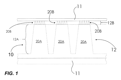
DESCRIPTION OF THE DRAWINGS
[0019] Fig. 1 is a schematic view of a dielectric between conductive
plates of a
capacitive-based tactile sensor in accordance with an embodiment of the
present
disclosure;
[0020] Fig. 2 is a enlarged side view showing the geometry of the
dielectric of
Fig. 1 as taken with an SEM microscope;
[0021] Fig. 3 is a picture of a resulting mold 30 as well as close up 3D
views
taken with an optodigital microscope;
[0022] Fig. 4 shows graphs pertaining to the permittivity of a composite
of the
dielectric of Fig. 1 for different volume fractions of BaTiO 3 and PMN-PT; and
[0023] Fig. 5 are schematic view of a manufacturing process for the
dielectric of
Fig. 1.
DETAILED DESCRIPTION
[0024] Referring to the drawings and more particularly to Fig. 1, a
sensor part of a
capacitive-based tactile sensor is shown at 10, and comprises a pair of spaced
apart
conductive plates 11 with a dielectric 12 therebetween. The capacitive-based
tactile
sensor 10 may be part of any appropriate apparatus, such as a robotic arm,
robotic
hand, manipulator, among many other possible applications. The conductive
plates
11 are wired to a controller, which controller is not shown herein for
simplicity.
[0025] The dielectric 12 of the sensor 10 is microstructured, but at a
relative large
magnitude so as to simplify the manufacturing process, for instance by the
fact that
specialized equipment may not be required, other than a CO2 laser for
instance. As
described hereinafter, the permittivity of the dielectric 12 may also be
increased by
embedding nanoparticles of ferroelectric ceramics in the silicone or like
polymeric
material used for the dielectric 12.
[0026] According to [6, 7, 8], in order to be comparable to a human hand,
a tactile
sensor should be capable of measuring forces up to 10 N on a surface of 1 cm 2
(100 Kpa). To achieve fine manipulations, it is also important that the sensor
remain
sensitive in the range under 1 N [9] on the same area. To satisfy these two
constraints that may be considered contrary from a technical point of view
(sensing
a considerable range of forces but also being sensitive to very low forces),
the
dielectric 12 has a microstructure of a plurality of members conductively
extending
4
CA 02898763 2015-07-21
WO 2014/110683
PCT/CA2014/050040
between the conductive plates. Each of the members has at least two layers (or
stages) of different sized features, namely stages 12A and 12B. It is
considered to
have additional stages, such as a third stage, a fourth stage, etc. The first
stage
12A is composed of conic features 20A of a base diameter of 900 p m at a first
end
surface, although this base diameter may be within an acceptable range. In
this non-
!imitative embodiment, the apex of the conic features 20A is at about 5 mm,
but the
height of the conic features is truncated at 800 p m, defining a frusto-
conical
geometry. Other geometries are considered as well, one of which is a
cylindrical
geometry, and others including prisms and pyramids. Moreover, it is pointed
out
that the frusto-conical geometry is not perfect as shown in the large scale of
Figs. 1
and 2 due to the manufacturing process, i.e., but reference will nonetheless
be
made to a frusto-conical geometry in spite of the pseudo-cone shape (or pseudo-
cylinder, etc).
[0027] Due to their size and density over the surface (e.g., 64 per cm 2
), the conic
features 20A account for significant variation of the distance d between the
two
conductive plates 11 of the capacitive sensor 10 over most of the range of the
possible applied pressure (10-100 Kpa). In order to increase the sensitivity
of the
sensor to the lower pressure range, on top of each of these truncated conic
features
20A lies conic features 20B, of smaller base diameter, as projecting from an
end
surface of the conic feature 20A. As illustrated in Figs. 1 and 2, the conic
features
20B may be smaller cones or pseudo-cones. In the illustrated embodiment of
Fig. 2,
the conic features 20B may have a base diameter of about 80 p m and apex of
about 100 pm. By being relatively easy to deform upon being exposed to
pressures, the conic features 20B increase the variation of the distance d of
eq. (1)
for low applied stress values. However, their effect is negligible for higher
stresses
as the conic features 20B rapidly reach their maximum deformation. In similar
fashion to the features 20A, the features 20B may have different geometries,
one of
which is a cylindrical geometry (or pseudo-cylinders). Accordingly, the
diameter of
the feature 20A at its surface interfaced with the base of the features 20B is
greater
than the sum of diameters of at least two features 20B. This interfaced
surface is
theoretical, as the features 20B are monolithically integral with the feature
20A. The
feature 20A of the first stage 12A therefore has a height (i.e., in the
distance c/) that
is substantially greater than a height of the second features 20B of the
second stage
12B. For instance, a ratio of height ranging between 3:1 to 30:1 is well
suited for the
CA 02898763 2015-07-21
WO 2014/110683
PCT/CA2014/050040
dielectric 12.
Likewise, a cross-section area of the second features 20B is
substantially smaller than a cross-section area of the first feature 20A, at
the
interfaced surface therebetween. For example, a ratio of cross-section areas
ranging between 3:1 to 40:1 is well suited for the dielectric 12.
[0028] The
microstructured dielectric 12 is made of a soft material (e.g., 30 on the
00 scale of Shore hardness), such as platinum cured silicone (Ecoflex 00-30,
Smooth-On) cast in an acrylic mold. The mold may be engraved using a
conventional CO2 laser (e.g., Epilog Helix 40 watts). In some conditions, the
maximum effective resolution of the laser cutter in the acrylic is 600dpi.
Indeed, due
to the spot size of the laser as well as the heat diffusion in the mold
material it may
be difficult to engrave any features smaller than the size associated with
this
resolution. The base diameter of the smallest features 20B is closely related
to this
limitation. By controlling the speed of the machine as well as the power of
the laser
the desired height of the features 20B as well as the desired cone angle may
be
achieved. Following multiple experiments, rastering the acrylic in a single
pass with
a laser power of 90% and speed of 25% gave the desired depth of the mold (900
pm) and suitable results in terms of sharpness. For illustrative purposes,
Fig. 3
shows a picture of a resulting mold 30 as well as close up 3D views taken with
an
optodigital microscope (Olympus DSX100). Moreover, Fig. 5 shows a series of
steps that may be used to manufacture the dielectric 12 with the mold 30. It
is
shown that the numerous members may be interconnected by a base sheet, with
the
base sheet and members forming one monolithic body for the dielectric 12, with
or
without additives, and additional components such as the conductive fibers in
the
base sheet as in Fig. 5.
[0029] The
microstructured configuration of the dielectric 12 of Fig. 1 has lowered
the material stiffness and reduced the hysteresis arising from the
incompressibility of
silicones, as compared with existing configurations. To increase the pressure
sensitivity of the capacitive-based tactile sensor 10, the static relative
permittivity of
the dielectric material may also be increased, thereby increasing the
dielectric
constant of the material to improve the signals-to-noise ratio. According to a
first
reason, for a given applied pressure, although the relative change in
capacitance
AC /C0 may be the same, increasing the dielectric constant will increase the
magnitude of the capacitance AC. Most off-the-shelf capacitance-to-digital
converters (CDC) work based on time measurement of a response of the capacitor
6
CA 02898763 2015-07-21
WO 2014/110683
PCT/CA2014/050040
to an excitation signal [10]. The time is measured with a range that is
limited in
resolution. Therefore, up to a certain range, the greater the variation in
Farads of the
capacitance is, the higher the count will be, thus increasing the signals-to-
noise
ratio.
[0030] According
to a second reason, numerous capacitive-based tactile [1, 2, 4,
3, 11] that have been proposed in literature consider the pressure measurement
as
a direct function of the change in the distance d between the two plates of
the
capacitor, i.e.
A
Pax 6 So __________________________________________________________ (2)
=
r d(Pa)
[0031] This is
assuming that there is no interaction between the deformation of
the dielectric and the static relative permittivity of the material. For
tactile sensors
using plain silicone sheets or closed-cells foam as a dielectric, this is a
valid
approximation. However, with the microstructure of the dielectric 12, the
static
relative permittivity will vary as the proportion of air vs material in a
given volume
changes with the applied pressure. In this case the pressure measurement
becomes
A
Pax er(Pa)6o- = (3)
d(Pa)
[0032] This
characteristic increases the non-linearity of the response but also the
capacitance variation for a given load and thus the sensitivity of the sensor.
In order
to maximize this effect, a high relative permittivity of the material used in
the
dielectric of the sensor may be desirable to increase the variation between
the
overall dielectric constant under no load and maximum load.
[0033] The
dielectric constant of typical polymers is generally below 5. In order to
increase this property, a high-permittivity nanoparticles of ferroelectric
ceramic may
be embedded in the silicone of the dielectric 12. Nanoparticles of
ferroelectric
ceramic have been embedded in epoxy [12], polyurethane [13], polyamide [14],
polydimethylsiloxane (PDMS) [15] and other silicones [16] for this purpose.
[0034] One
filler that may be used for increasing the dielectric constant of the
silicone in the dielectric 12 is calcium copper titanate [17] (CCTO, CaCu 3 Ti
4 012)
due to its high dielectric constant (Sr >250000) [18]. Other alternatives are
barium
7
CA 02898763 2015-07-21
WO 2014/110683
PCT/CA2014/050040
titanate (BaTiO3) and lead magnesium niobate-lead titanate (PMN-PT,
Pb(Mg1,3Nb2,3)03-PbTiO3) nanopowder that have also a high dielectric constant.
These two ferroelectric ceramics have been commonly used in the manufacturing
of
capacitors with high capacitance values and therefore are cost-effective
solutions.
[0035] In an embodiment, to increase the permittivity of the dielectric
material,
nanoparticles of BaTiO3 of 200nm size and tetragonal-like shape have been used
(e.g., US Research Nanomaterials Inc.), as have spherical microparticles of
PMN-
PT of 3,u m (TRS Ceramic Inc. under the name PMN-38 ). According to the
specification, these materials have a dielectric constant at room temperature
of 4000
and 19 000 respectively. Figure 4, provided as a non-limitative example, shows
the
values of the dielectric constants experimentally obtained for different
volume
fractions of BaTiO3 and PMN-PT embedded the silicone matrix, for illustrative
purposes. These values where calculated according to eq.(1) using the
capacitance
measured at 100hz with a LCR meter (B&K Precision 878B) of different
dielectric
samples of a known area and thickness (4 cm2 and 2 mm respectively). Fig. 4
suggests a quasi-linear relation between the volume fraction of filler and the
dielectric constant of the composite. These values are also similar to reports
in [20,
15, 21, 22, 23] for similar particles into a similar crosslinked matrix of
silicone.
Considering the high permittivity of the ceramic particles used, the
dielectric
constant value obtained for the composite may seem low. The resulting
dielectric
constant of a composite is not a simple function of the volume proportion
between
the polymer matrix and the filler. According to [23, 24, 25] this is due to
the fact that
a single crystal of the ceramics particles does not have the same permittivity
along
all 3 axes. For example the permittivity of a single crystal of BaTiO3 has a
permittivity of 4000, 100, and 100 along the a, b, and c axes, respectively.
Since
these particles are randomly aligned in the polymer matrix, the resulting
permittivity
is low.
[0036] The electrical property of the material used as a dielectric may
be
increased to characterize the performance of the sensor 10. The compliance of
the
dielectric material needs to be taken into account. If the electrical property
of the
composite is the sole consideration, PMN-PT may be a suitable choice according
to
the data shown in Fig. 4. In order to take into account the mechanical side of
the
problem, tests may be performed to characterize the relation between the
stress
8
CA 02898763 2015-07-21
WO 2014/110683
PCT/CA2014/050040
applied and the capacitance variation. Figure 4 show the capacitance variation
AC
for different volume fractions and for two different stresses (10 KPa and 100
KPa) as
well as the relative change of capacitance AC /C0 for the same
characteristics. This
data was obtained with a force test stand (Mark-10 ES20,) equipped with force
and
displacement gauges (Mark-10 M4-10 and Mitutoyo 543-693, respectively) and the
capacitance data was recorded with the above-referred LCR meter. These tests
have been performed on the microstructured dielectric 12 created with the mold
30
of Fig. 3 on a taxel size of 64 mm2. Despite the advantage of PMN-PT seen in
Fig. 4 for the dielectric constant, the graphs presented in Fig. 4 show that
the
capacitance variation and the relative change in capacitance are almost the
same
for the two different composites at 10 KPa and 100 KPa. BaTiO3 may
advantageously be used as a filler due to its cost being lower than that of
PMN-PT
and due to some hysteresis observed on sensors using PMN-PT filled dielectric.
9
CA 02898763 2015-07-21
WO 2014/110683
PCT/CA2014/050040
REFERENCES
[1] M.Leineweber,G.Pelz,M.Schmidt,H.KappertandG.Zimmer,"New tactile sensor
chip
with silicone rubber cover," Sensors and Actuators A: Physical, vol. 84, no.
3, pp. 236-245,
2000.
[2] A.Schmitz,M.Maggiali,L.Natale,B.Bonino,andG.Metta,"Atactile sensor for the
fingertips
of the humanoid robot icub," in In IEEE/RSI International Conference on
Intelligent Robots
and Systems, 2010.
[3] T. Hoshi and H. Shinoda, "Robot skin based on touch-area-sensitive tactile
element," in
Robotics and Automation, 2006. ICRA 2006. Pro-
ceedings2006IEEEIntemationalConferenceon. Ieee,2006,pp.3463¨ 3468.
[4] J. Ulmen and M. Cutkosky, "A robust, low-cost and low-noise artificial
skin for human-
friendly robots," in Robotics and Automation (ICRA), 2010 IEEE International
Conference
on. IEEE, 2010, pp. 4836-4841.
[5] S. Mannsfeld, B. Tee, R. Stoltenberg, C. Chen, S. Barman, B. Muir, A.
Sokolov, C.
Reese, and Z. Bao, "Highly sensitive flexible pressure sensors with
microstructured rubber
dielectric layers," Nature Materials, vol. 9, no. 10, pp. 859-864,2010.
[6] J. Dargahi and S. Najarian, "Human tactile perception as a standard for
artificial tactile
sensinga review," The International Journal ofMedical Robotics and Computer
Assisted
Surgery, vol. 1, no. 1, pp. 23-35,2004.
[7] E. Dellon, K. Keller, V. Moratz, and A. Dellon, "The relationships between
skin
hardness, pressure perception and two-point discrimination in the fingertip,"
The Journal of
Hand Surgery: British & European Volume, vol. 20, no. 1, pp. 44-48,1995.
[8] H. Ehrsson, A. Fagergren, and H. Forssberg, "Differential fronto-parietal
activation
depending on force used in a precision grip task: an fmri study," Journal of
Neurophysiology,
vol. 85, no. 6, pp. 2613-2623,2001.
[9] G. Westling and R. Johansson, "Responses in glabrous skin mechanore-
ceptors during
precision grip in humans," Experimental Brain Research, vol. 66, no. 1, pp.
128-140,1987.
[10] M. Gasulla, X. Li, and G. Meijer, "The noise performance of a high- speed
capacitive-
sensor interface based on a relaxation oscillator and a fast counter,"
Instrumentation and
Measurement, IEEE Transactions on, vol. 54, no. 5, pp. 1934-1940,2005.
[11] F. Castelli, "An integrated tactile-thermal robot sensor with capacitive
tactile array,"
Industry Applications, IEEE Transactions on, vol. 38, no. 1, pp. 85-90,2002.
[12] Y. Rao, S. Ogitani, P. Kohl, and C. Wong, "Novel polymer¨ceramic
nanocomposite
based on high dielectric constant epoxy formula for embedded capacitor
application,"
Journal ofApplied Polymer Science, vol. 83, no. 5, pp. 1084-1090,2001.
[13] S. Pyun, Y. Jin, and G. Lee, "Dielectric properties of pb (mg1/3nb2/3) o3-
pbtio3/polyurethane 0-3 composites," Journal of materials science letters,
vol. 21, no. 3, pp.
243-244,2002.
CA 02898763 2015-07-21
WO 2014/110683
PCT/CA2014/050040
[14] Z. Dang, Y. Lin, H. Xu, C. Shi, S. Li, and J. Bai, "Fabrication and
dielectric
characterization of advanced batio3/polyimide nanocomposite films with high
thermal
stability," Advanced Functional Materials, vol. 18, no. 10, pp. 1509-1517,
2008.
[15] D.KhastgirandK.Adachi,"Rheologicalanddielectricstudiesofaggre- gation of
barium
titanate particles suspended in polydimethylsiloxane," Polymer, vol. 41, no.
16, pp. 6403-
6413, 2000.
[16] B. Liu and M. Shaw, "Electrorheology of filled silicone elastomers,"
Journal of
Rheology, vol. 45, no. 3, pp. 641-657, 2001.
[17] S. Chung, I. Kim, and S. Kang, "Strong nonlinear current-voltage
behaviour in
perovskite-derivative calcium copper titanate," Nature ma- terials, vol. 3,
no. 11, pp. 774-
778, 2004.
[18] S. Guillemet-Fritsch, T. Lebey, M. Boulos, and B. Durand, "Dielectric
properties of
cacu3ti4o12 based multiphased ceramics," Journal of the European Ceramic
Society, vol. 26,
no. 7, pp. 1245-1257, 2006.
[19] Y. Yoneda, K. Sakaue, and H. Terauchi, "Dielectric investigation of
batio3 thin-film
capacitor," Japanese Journal of Applied Physics, vol. 39, p. 4839, 2000.
[20] D. Khastgir and K. Adachi, "Piezoelectric and dielectric properties of
siloxane
elastomers filled with bariumtitanate," Journal of Polymer Science Part B:
Polymer Physics,
vol. 37, no. 21, pp. 3065-3070, 1999.
[21] Y. Shen, E. Cherney, and S. Jayaram, "Electric stress grading of com-
posite bushings
using high dielectric constant silicone compositions," in Electrical
Insulation, 2004.
Conference Record of the 2004 IEEE International Symposium on. IEEE, 2004, pp.
320-323.
[22] C. Randall, S. Miyazaki, K. More, A. Bhalla, and R. Newnham, "Structural-
property
relationships in dielectrophoretically assembled ba- tio3 nanocomposites,"
Materials Letters,
vol. 15, no. 1, pp. 26-30, 1992.
[23] E. Cherney, "Silicone rubber dielectrics modified by inorganic fillers
for outdoor high
voltage insulation applications," Dielectrics and Electrical Insulation, IEEE
Transactions on,
vol. 12, no. 6, pp. 1108-1115, 2005.
[24] F. Carpi, D. De Rossi, and R. Kornbluh, Dielectric elastomers as
electromechanical
transducers: Fundamentals, materials, devices, mod- els and applications of an
emerging
electroactive polymer technology. Elsevier Science, 2008.
[25] V.TomerandC.Randall,"Highfielddielectricpropertiesofanisotropic polymer-
ceramic
composites," Journal of Applied Physics, vol. 104, no. 7, pp. 074 106-074 106,
2008.
[26] L. Qi, B. Lee, W. Samuels, G. Exarhos, and S. Parler Jr, "Three-phase
percolative
silver-batio3-epoxy nanocomposites with high dielectric constants," Journal of
applied
polymer science, vol. 102, no. 2, pp. 967- 971, 2006.
11