Note: Descriptions are shown in the official language in which they were submitted.
CA 02898925 2015-07-29
276826
DC POWER SYSTEM FOR MARINE APPLICATIONS
The present application claims priority to U.S. provisional patent application
Ser. No.
62/031,402 filed July 31, 2014, and U.S. provisional patent application Ser.
No.
62/053,400 filed September 22, 2014.
BACKGROUND
Embodiments of the invention relate generally to a direct current (DC) power
system and
more specifically to a DC power system for marine applications.
In the last few decades, marine traffic has increased substantially across the
world due to
tremendous rise in cargo transport vessels, warships, offshore oil ships,
passenger ships
etc. These vessels or ships have many electrical loads on board. Variable
speed electric
drives for pumps, fans, electric propulsion installations, lighting and air
conditioning are
some examples of the electrical loads on board of a ship. The electrical loads
operate at
various different voltages and frequencies, and thus need separate electric
power supplies.
Most of the ships use alternating current (AC) power system architecture.
However,
more recently some ships are using DC power system architecture including
energy
storage devices or electrical generators to meet the demands of the plurality
of electrical
loads. If a load needs alternating current (AC) power supply, the DC power may
be
converted into AC power with help of power electronic converters. Similarly,
if the
electrical generator is AC then the AC power may be converted into DC power
via power
electronic converters. Generally, a plurality of generators supplies power to
a plurality of
DC buses which in turn supply power to a particular electrical load. There are
examples
where a single DC bus can also provide power to the entire ship electrical
load.
Challenges with conventional DC power system include integration of multiple
DC buses
with different voltage levels, isolating the faults in the DC power system in
a very short
time and integrating the various energy storage devices and generators. For
these and
other reasons, there is a need for the present DC power system for marine
applications.
1
CA 02898925 2015-07-29
276826
BRIEF DESCRIPTION
In accordance with an embodiment of the present technique, a power system for
a marine
ship is provided. The power system includes a plurality of protection zones
wherein each
protection zone comprises a plurality of direct current (DC) buses and a
plurality of
power converters. Furthermore, at least two DC buses of two protection zones
are
coupled to each other via a bus-tie converter. A controller is provided to
control the
operation of the plurality of power converters and the at least one bus-tie
converter. The
bus-tie converter includes at least two converter legs coupled by at least one
inductor.
Each converter leg comprises a first branch having two outer switching devices
and at
least one inner switching device connected between the two outer switching
devices. The
first branch also includes a damping resistor coupled between the two outer
switching
devices to dissipate a fault current. Further, each converter leg comprises a
snubber
circuit having a combination of a diode, a resistor and a capacitor.
In accordance with another embodiment of the present technique, a method of
providing
power to a marine ship is disclosed. The method includes providing a plurality
of
protection zones including a plurality of power converters and connecting a
bus-tie
converter between at least two DC buses of two protection zones. In the
provided
method, connecting the bus-tie converter comprises providing at least two
converter legs
coupled by at least one inductor. Furthermore, providing each converter legs
comprises
forming a first branch by connecting at least one inner switching device
between two
outer switching devices; connecting a damping resistor in series with at least
one inner
switching device to dissipate a fault current and forming a snubber circuit
with a
combination of a diode, a resistor and a capacitor.
DRAWINGS
FIG. 1 is a diagrammatical representation of a power system for a marine ship,
according
to aspects of the present disclosure;
2
CA 02898925 2015-07-29
276826
FIG. 2 is a diagrammatical representation of a detailed view of a bus-tie
converter of FIG.
1, according to aspects of the present disclosure;
FIGs. 3a and 3b are schematic diagram representations of operation of the bus-
tie
converter, according to aspects of the present disclosure;
FIG. 4 is another diagrammatical representation of a detailed view of a bus-
tie converter
of FIG. 1, according to aspects of the present disclosure; and
FIG. 5 is yet another diagrammatical representation of a detailed view of a
bus-tie
converter of FIG. 1, according to aspects of the present disclosure.
DETAILED DESCRIPTION
Unless defined otherwise, technical and scientific terms used herein have the
same
meaning as is commonly understood by one of ordinary skill in the art to which
this
disclosure belongs. The terms "first", "second", and the like, as used herein
do not
denote any order, quantity, or importance, but rather are used to distinguish
one element
from another. Also, the terms "a" and "an" do not denote a limitation of
quantity, but
rather denote the presence of at least one of the referenced items. The term
"or" is meant
to be inclusive and mean one, some, or all of the listed items. The use of
"including,"
"comprising" or "having" and variations thereof herein are meant to encompass
the items
listed thereafter and equivalents thereof as well as additional items.
Furthermore, the
terms "circuit" and "circuitry" and "controller" may include either a single
component or
a plurality of components, which are either active and/or passive and are
connected or
otherwise coupled together to provide the described function.
Turning now to the drawings, by way of example in FIG. 1, a power system 100
for a
marine ship is depicted. In one embodiment, the power system 100 may include
two
protection zones 102 and 104 coupled via bus-tie converters 106 and 188.
However, in
other embodiments, there may be many such protection zones which are connected
to
each other via a plurality of bus-tie converters. As will be appreciated by
those skilled in
3
CA 02898925 2015-07-29
276826
the art, protection zones are created to limit the extent to which a power
system may be
disconnected during a fault. The protection zone in the Marine ship may
include energy
sources, DC buses and a plurality of converters to feed power to various
loads. The
energy sources may be AC or DC generators, energy storage devices and the
loads may
include lighting loads or variable frequency drives, for example. In the
embodiment
shown, protection zone 102 includes energy sources such as AC generators 108,
110 and
an energy storage device 112 and protection zone 104 includes energy sources
such as
AC generators 114, 116 and an energy storage device 118.
Furthermore, in protection zone 102, AC generators 108, 110 feed power to a DC
bus 120
via power electronic converters 122 and 124 respectively, and energy storage
device 112
feeds power to a DC bus 126 via a power electronic converter 128. Power
electronic
converters 122, 124 are AC to DC converters as they have to convert power from
AC
generators to the DC bus whereas power electronic converter 128 is a DC to DC
converter as it couples a DC energy storages device to a DC bus. The two DC
buses 120
and 126 do not have same DC voltage and hence are coupled to each other via a
DC to
DC converter 130. DC to DC converter 130 may be a bidirectional DC to DC
converter
or an unidirectional DC to DC converter. Further, loads 132 and 134 are
connected to
DC bus 120 via power electronic converters 136 and 138 respectively and loads
140 and
142 are connected to DC bus 122 via power electronic converters 144 and 146
respectively. Depending on whether the load is an AC load or a DC load, power
electronic converter 136, 138, 144 and 146 may be AC to DC converters or DC to
DC
converters.
In similar manner, in protection zone 104, AC generators 114, 116 feed power
to a DC
bus 150 via power electronic converters 152 and 154 respectively, and energy
storage
device 118 feeds power to a DC bus 156 via a power electronic converter 158.
The two
DC buses 150 and 156 are coupled to each other via a DC to DC converter 160.
DC
Furthermore, loads 162 and 164 are connected to DC bus 150 via power
electronic
converters 166 and 168 respectively and loads 170 and 172 are connected to DC
bus 152
4
CA 02898925 2015-07-29
276826
via power electronic converters 174 and 176 respectively. Based on the type of
load i.e.,
an AC load or a DC load, power electronic converter 166, 168, 174 and 176 may
be AC
to DC converters or DC to DC converters. It should be noted that in the
embodiment
shown, all converters have been shown to have only one input terminal and one
output
terminal for ease of explanation. However, a negative terminal or a reference
terminal is
always there at the input and the output of each of the converter.
Power System 100 further includes a controller 180 to control the operation of
bus-tie
converters 106, 188 and other converters in protection zones 102 and 104. It
should be
noted that even though a single controller 180 is shown in the embodiment of
FIG. 1, in
other embodiments controller 180 may be split into a plurality of controllers
and each
individual controller may control a part of the power system 180. Power system
100 may
also include passive devices such as fuses and/or circuit breakers (not shown)
to protect a
second of the power system 100 during a fault (e.g., short circuit fault). In
one
embodiment, controller 180 blocks propagation of a fault from one DC bus to
another DC
bus based on the coordination between the bus-tie converter, the passive
devices and
other power electronic and/or DC to DC converters.
For example, if there is a fault on DC bus 126 or the subsequent branches
connected to it
(e.g., branches 182, 184, 186 in FIG. 1), then controller 180 would block
propagation of
that fault (i.e., one fault creating another fault) from DC bus 126 to DC bus
120. It
should be noted that the fault may be detected by controller 180 if an output
current of
converter 130 exceeds a fault current magnitude threshold or if an output
voltage of
converter 130 breaches a fault voltage magnitude threshold. During the fault
on DC bus
126, controller 180 would operate DC to DC converter 130 which is feeding
power to DC
bus 126 in a current control mode and thus limits a fault current supplied by
DC bus 120
to DC bus 126. Once the fault is cleared by passive devices (e.g., fuse or
breaker) with
the help of controller 180 or otherwise, controller 180 will charge DC bus 126
to a rated
level. Once DC bus 126 is charged to the rated level, controller 180 will
switch back
operation of DC to DC converter 130 to a normal mode. In one embodiment, the
normal
CA 02898925 2015-07-29
276826
mode of DC to DC converter 130 refers to a voltage control mode. However, if
the fault
sustains for a certain amount of time, which indicates a permanent fault on
the bus and
not a transient one, controller 180 will stop the operation of DC/DC converter
130 and
notify the upstream system. Contrclier 180 would similarly control other
converters so as
to block propagation of the fault from one bus to another bus.
In one embodiment of the present technique, a second bus-tie converter 188 may
be used
to connect low voltage buses 126 and 156. In other words, protection zones 102
and 104
may be coupled to each other via two bus-tie converters 106 and 188. Bus-tie
converter
106 couples medium voltage buses 120 and 150 and bus-tie converter 188 couples
low
voltage buses 126 and 156. It should be noted that low voltage buses 126 and
156
operate at a low voltage with respect to medium voltage buses 120 and 150
respectively.
This embodiment allows low voltage buses 126 and 156 and their corresponding
branches to operate normally even if one of the medium voltage buses 120 or
150 is
faulty and unable to supply any power.
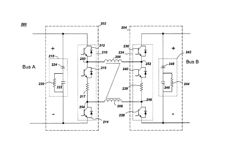
FIG. 2 shows a detailed view of a bus-tie converter 200 such as bus-tie
converters 106
and 188 of FIG. 1 in accordance with an embodiment of the present technique.
In one
embodiment, bus-tie converter 200 is coupled between two buses A and B of two
protection zones 102 and 104 respectively. In other words, bus-tie converter
200 is
directly connected between the buses A and B. The bus-tie converter 200
includes a first
converter leg 202 and a second converter leg 204 coupled by at least one
inductor 206,
208.
First converter leg 202 includes a first branch 210 having two outer switching
devices
212, 214 and one inner switching device 216. The inner switching device 216 is
connected between the two outer switching devices 212, 214. A damping resistor
217 is
also connected between the two outer switching devices 212 and 214. The
damping
resistor 217 is connected in series with the inner switching device 216. First
converter
leg 202 further includes a snubber circuit 218 having a resistor 220 and a
capacitor 222
6
CA 02898925 2015-07-29
276826
connected in parallel. The snubber circuit 218 further includes a diode 224
connected in
series with a parallel circuit of resistor 220 and capacitor 222.
Similarly, second converter leg 204 includes a first branch 234 having one
inner
switching device 240 connected between two outer switching devices 236, 238.
Second
converter leg 204 also includes a damping resistor 239 connected in series
with the inner
switching device 240. The damping resistor 239 is connected between outer
switching
devices 236, 238. Second converter leg 204 further includes a snubber circuit
242 having
a resistor 244 and a capacitor 246 connected in parallel and further the
combination being
connected in series with a diode 248.
As discussed earlier, the first converter leg 202 and the second converter leg
204 are
coupled to each other by inductors 206 and 208. In one embodiment, inductor
206 is
connected between nodes 250, 252, wherein node 250 is formed by an
interconnection of
outer switching device 212 and inner switching device 216 and node 252 is
formed by an
interconnection of outer switching device 236 and inner switching device 240.
Similarly,
inductor 208 is connected between nodes 254, 256, wherein node 254 is formed
by an
interconnection of outer switching device 214 and inner resistor 217 and node
256 is
formed by an interconnection of outer switching device 238 and inner resistor
239. It
should be noted that the position of inner resistor 217, 239 and inner
switching device
216, 240 is interchangeable and so accordingly the node formation may vary.
In one embodiment, the switching devices 212, 214, 216, 236, 238, 240 may
include
controllable semiconductor switches. The controllable semiconductor switches
include
an insulated gate bipolar transistor (IGBT), a metal oxide semiconductor field
effect
transistor (MOSFET), a field effect transistor (FET), a gate turn-off
thyristor, an insulated
gate commutated thyristor (IGCT), an injection enhanced gate transistor
(IEGT), a silicon
carbide based switch, a gallium nitride based switch, a gallium arsenide based
switch, or
equivalents thereof. Furthermore, when the controllable semiconductor switches
open an
inductive circuit made up of bus parasitic inductances in buses A and B, the
energy in
these parasitic inductance will be absorbed by the snubber circuits 218, 242
respectively.
7
CA 02898925 2015-07-29
276826
Therefore, the snubber circuits 218 and 242 provide an alternative current
path for the
inductor current and the generated voltage spike L di/dt is reduced. Thus, the
voltage
spike generated across these switching devices because of sudden change of
inductive
current (i.e., L di/dt) is reduced. Snubber circuits 218, 242 also maintain
the respective
bus voltage to a normal operating value when there is a fault in the other
protection zone.
Diodes 224, 248 in snuber circuits '18, 242 ensure that in case of fault on
their respective
buses, the snubber capacitors 222, 246 do not discharge into the fault, rather
the
capacitors 222, 246 discharge via resistors 220, 244 respectively.
Figs. 3a and 3b show the operation of the bus-tie converter 200 of Fig. 2
during a normal
condition and a fault condition respectively. During normal operation,
controller 180
(Fig. 1) sends control signals to switch on the outer switching devices 212,
214 and 236,
238 of legs 202 and 204 respectively. Thus, during normal condition, the power
transfer
between the two buses A and B of two different protection zones is facilitated
by
switching devices 212, 236, 214, 238 and inductors 206, 208 respectively. In
the
embodiment shown in Fig. 3a, the power transfer is facilitated from bus A to
bus B as
shown by current 302. Since outer switching devices 236, 238 are connected in
opposite
polarity with respect to current 302, the antiparallel diodes of outer
switching devices 236
and 238 conduct to carry the current 302.
In the embodiment shown in Fig. 3b, there is a short circuit fault on bus B.
During such a
fault condition the controller sends controls signals to switch off outer
switching devices
212, 214, 236 and 238. The controller further sends control signals to switch
on inner
switching devices 216 and 240. During the time outer switching devices 212,
214, 236
and 238 are turning off after receiving the control signals, inductors 206,
208 limit the
fault current. After the outer switching devices 212, 214, 236 and 238 are
switched off; a
circulating current 304 may flow between the antiparallel diode of inner
switching device
216 and the inner switching device 240. The circulating current 304 dissipates
energy
stored in the inductors 206, 208 into damping resistors 217, 239. The fault
current 306
then may flow between antiparallel diodes of outer switching devices 236, 238,
and
8
CA 02898925 2015-07-29
276826
antiparallel diode of inner switching device 240. As the energy in inductors
206, 208 is
dissipated, the circulating current 304 also decays down and there will be no
current in
inner switching devices 216. This results in complete isolation of the two
buses, bus A
and bus B of two different protection zones. The fault current on bus B may
then be
decayed to a reduced value by damping resistor 239. Further, the snubber
capacitor 222
then may get charged to the rated bus voltage by a current 308 from bus A.
FIG. 4 shows another detailed view of a bus-tie converter 400 such as bus-tie
converters
106 and 188 of FIG. 1 in accordance with an embodiment of the present
technique. In the
embodiment shown, inner switching devices 216 and 240 of Fig. 2 are replaced
with
diodes 402 and 404 respectively. In this case, when the outer switching
devices are 212,
214, 236, 238 are turned off during a fault on bus B, no circulating current
flows between
diodes 402, 404. Thus, to dissipate the energy stored in inductors 206 and
208, a current
406 flows through inductors 206, 208, damping resistor 217, diode 402 and
antiparallel
diodes of outer switching devices 236, 238.
FIG. 5 shows yet another view of a bus-tie converter 500 in accordance with an
embodiment of the present technique. The but-tie converter 500 in FIG. 5 is
similar to
the bus-tie converter 400 in FIG. 4 except for the damping resistor
configuration.
Damping resistors 217 and 239 of the bus-tie converter 400 are fixed
resistors. On the
contrary damping resistors of bus-tie converter 500 shown by blocks 506, 512
are
variable resistors. Variable damping resistor 506 includes a fixed resistor
510 connected
in parallel with a controllable semiconductor device 508. Similarly, variable
damping
resistor 512 includes a fixed resistor 514 connected in parallel with a
controllable
semiconductor device 516. By varying conduction time of controllable
semiconductor
devices 508 and 516, currents in fi ed resistors 510 and 514 can be
controlled. Thus, an
average resistance value of variable damping resistors 506 and 512 can be
controlled and
the dissipation of energy in the inductors can be controlled.
Advantages of the present technique include ability to disconnect the two
protection
zones extremely fast during a fault scenario. Furthermore, since the two zones
are
9
CA 02898925 2015-07-29
276826
coupled during normal operation, energy storage elements, the different zones
can share
the same energy storage.
While there have been described herein what are considered to be preferred and
exemplary embodiments of the present invention, other modifications of these
embodiments falling within the scope of the invention described herein shall
be apparent
to those skilled in the art.
=