Note: Descriptions are shown in the official language in which they were submitted.
CA 02898934 2015-07-30
269604
MODULAR MULTI-LEVEL POWER CONVERSION SYSTEM WITH
DC FAULT CURRENT LIMITING CAPABILITY
CROSS REFERENCE TO RELATED APPLICATIONS
[0001] This application is a continuation-in-part of US Patent Application
No.
13/484517, entitled "MULTI-LEVEL POWER CONVERTER," filed on May 31, 2012,
which is herein incorporated by reference.
BACKGROUND
[0002] Embodiments of the present disclosure are related to power
conversion
systems, and more particularly to a multi-level power conversion system.
[0003] Power conversion systems are often used to convert alternating
current (AC)
power to direct current power (DC) at a transmitting substation and to convert
the
transmitted DC power back to AC power at a receiving substation in high
voltage direct
current (HVDC) transmissions. In one approach, such power conversion systems
have a
modular multi-level structure. The modular multi-level structure includes a
stacked
arrangement of power converter modules for converting AC power to DC power and
DC
power to AC power.
[0004] Various designs of power converter modules have been employed to
form
modular multi-level power conversion systems. One such design of the power
converter
modules includes a half bridge which in turn includes two switches coupled
across a
capacitor. Such a half bridge module is susceptible to DC faults, for example,
a DC short
circuit. Moreover, the half bridge module is incapable of limiting such short
circuit
currents.
[0005] Furthermore, a full bridge power converter module has been employed
to
overcome the shortcomings of the half bridge module. The full bridge power
converter
module, while capable of limiting the DC short circuit current, entails use of
twice the
1
CA 02898934 2015-07-30
269604
number of switches as the half bridge structure. Such an increased number of
switches
result in higher losses and costs.
[0006] Additionally, a double clamped power converter module has also been
employed to limit the short circuit current. Switches in the double clamped
power
converter module have a power rating between the power ratings of the switches
of the
half bridge power converter module and the full bridge power converter module.
However, the double clamped power converter module includes additional
electronic
components in comparison to the full bridge power converter module. Use of
these
additional electrical components leads to higher costs and complexities in a
modular
approach.
[0007] Lately, another approach has been used to design the power converter
module.
This approach includes two switches and two capacitors in each power converter
module.
Such a power converter module allows easier insulation and better cooling
during
operation. However, this configuration fails to limit the short circuit
current under DC
fault conditions.
BRIEF DESCRIPTION
[0008] In accordance with an aspect of the present disclosure, a power
converter
module is provided. The power converter module includes a first converter leg
and a
second converter leg. The first converter leg includes a first switching unit
and a second
switching unit coupled in series. The second switching unit is disposed in a
reverse
orientation with respect to an orientation of the first switching unit. The
second converter
leg includes a third switching unit and a diode coupled in series. The third
switching unit
is disposed in a reverse orientation with respect to the orientation of the
first switching
unit. The power converter module also includes a first energy storage device
operatively
coupled between the first converter leg and the second converter leg. The
power
converter module further includes a second energy storage device operatively
coupled
between the first converter leg and the second converter leg.
2
CA 02898934 2015-07-30
269604
[0009] In accordance with another aspect of the present disclosure, a power
conversion system is provided. The power conversion system includes a
plurality of
phase units, where each phase unit is configured to convert power
corresponding to a
respective phase of an input power. Also, each phase unit includes a plurality
of power
converter modules coupled in series to each other. Moreover, each power
converter
module includes a first converter leg and a second converter leg. The first
converter leg
includes a first switching unit and a second switching unit coupled in series.
The second
switching unit is disposed in a reverse orientation with respect to an
orientation of the
first switching unit. The second converter leg includes a third switching unit
and a diode
coupled in series. The third switching unit is disposed in a reverse
orientation with
respect to the orientation of the first switching unit. The power converter
module also
includes a first energy storage device and a second energy storage device
operatively
coupled between the first converter leg and the second converter leg.
[0010] In accordance with yet another aspect of the present disclosure, a
method for
converting power is provided. The method includes coupling a first switching
unit and a
second switching unit in series to form a first converter leg, where the
second switching
unit is disposed in a reverse orientation with respect to an orientation of
the first
switching unit. The method also includes coupling a third switching unit and a
diode
coupled in series to form a second converter leg, where the third switching
unit is
disposed in a reverse orientation with respect to the orientation of the first
switching unit.
The method further includes operatively coupling a first energy storage device
and a
second energy storage device between the first converter leg and the second
converter leg
to form a power converter module. The method also includes operatively
coupling a
plurality of power converter modules to form a power conversion system
configured to
convert an input power to an output power. The method further includes
limiting a fault
condition in the power conversion system upon identifying the fault condition
to
minimize a DC fault current in the power conversion system.
3
CA 02898934 2015-07-30
269604
DRAWINGS
[0011] These and other features, aspects, and advantages of the present
invention will
become better understood when the following detailed description is read with
reference
to the accompanying drawings in which like characters represent like parts
throughout the
drawings, wherein:
[0012] FIG. 1 is a schematic representation of a high voltage direct
current (HVDC)
transmission system, according to aspects of the present disclosure;
[0013] FIG. 2 is a schematic representation of a power converter module
employed in
forming a power conversion system for use in the HVDC transmission system of
FIG. 1,
according to aspects of the present disclosure;
[0014] FIG. 3 is a schematic representation of a power converter module
configured to
provide a positive voltage across electrical terminals of a power converter
module,
according to aspects of the present disclosure;
[0015] FIG. 4 is a schematic representation of a power converter module
configured to
provide zero voltage across electrical terminals of a power converter module,
according
to aspects of the present disclosure;
[0016] FIG. 5 is a schematic representation of a power converter module
configured to
provide a negative voltage across electrical terminals of a power converter
module,
according to aspects of the present disclosure;
[0017] FIG. 6 is a schematic representation of another embodiment of a
power
converter module, according to aspects of the present disclosure;
[0018] FIG. 7 is a schematic representation of yet another embodiment of a
power
converter module, according to aspects of the present disclosure; and
4
CA 02898934 2015-07-30
269604
[0019] FIG. 8 is a flow chart representing a method for power conversion,
according
to aspects of the present disclosure.
DETAILED DESCRIPTION
[0020] Unless defined otherwise, technical and scientific terms used herein
have the
same meaning as is commonly understood by one of ordinary skill in the art to
which this
disclosure belongs. The terms "first", "second", and the like, as used herein
do not
denote any order, quantity, or importance, but rather are used to distinguish
one element
from another. Also, the terms "a" and "an" do not denote a limitation of
quantity, but
rather denote the presence of at least one of the referenced items, The term
"or" is meant
to be inclusive and mean one, some, or all of the listed items. The use of
"including,"
"comprising" or "having" and varia, ions thereof herein are meant to encompass
the items
listed thereafter and equivalents thereof as well as additional items. The
terms
"connected" and "coupled" are not restricted to physical or mechanical
connections or
couplings, and can include electrical connections or couplings, whether direct
or indirect.
Furthermore, the terms "circuit," "circuitry," "controller," and "processor"
may include
either a single component or a plurality of components, which are either
active and/or
passive and are connected or otherwise coupled together to provide the
described
function.
[0021] Aspects of the present disclosure are related to a power converter
module and a
power conversion system including the power converter module. In one
embodiment, the
power conversion system may include a high voltage direct current (HVDC)
transmission
system, a power distribution system, an electrical machine control system, or
a
combination thereof. The power conversion system includes a plurality of phase
units.
Moreover, each phase unit is configured to convert power corresponding to a
respective
phase of an input power. Furthermore, each phase unit includes a plurality of
power
converter modules coupled in series to each other.
CA 02898934 2015-07-30
269604
[0022] The power converter module may include a first converter leg and a
second
converter leg. The first converter leg may include a first switching unit and
a second
switching unit coupled in series. The second switching unit may be disposed in
a reverse
orientation with respect to an orientation of the first switching unit.
Furthermore, the
second converter leg may include a third switching unit and a diode coupled in
series.
The third switching unit may be disposed in a reverse orientation with respect
to the
orientation of the first switching unit. Moreover, the power converter module
may also
include a first energy storage device and a second energy storage device
operatively
coupled between the first converter leg and the second converter leg.
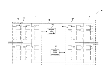
[0023] FIG. 1 is a schematic representation of a high voltage direct
current (HVDC)
transmission system 10, according to aspects of the present disclosure. The
HVDC
transmission system 10 may include an alternating current (AC) to direct
current (DC)
power conversion system 20 and a direct current (DC) to alternating current
(AC) power
conversion system 30 operatively coupled via a DC link 40. Hereinafter, the AC-
DC
power conversion system 20 may be referred to as a "source side power
conversion
system" and the DC-AC power conversion system 30 may be referred to as a "load
side
power conversion system." Moreover, the source side power conversion system 20
may
include a plurality of source side phase units 50 and the load side power
conversion
system 30 may include a plurality of load side phase units 60. Each of the
source side
phase units 50 may be configured to convert a respective phase of an AC power
to a DC
power. Similarly, each of the load side phase units 60 may be configured to
convert the
DC power to a respective phase of the AC power. In one embodiment, the
plurality of
source side phase units 50 may be operatively coupled in parallel. In another
embodiment, the plurality of load side phase units 60 may be operatively
coupled in
parallel. It may be noted that a number of phase units in the source side
power
conversion system 20 and the load side power conversion system 30 may
correspond to a
number of phases of the AC power. For example, converting a three phase AC
power
using the source side power conversion system 20 and the load side power
conversion
6
CA 02898934 2015-07-30
269604
system 30 may require three phase units in the source side power conversion
system 20
and three phase units in the load side power conversion system 30.
[0024] Furthermore, the plurality of source side phase units 50 may include
a plurality
of source power converter modules 55 operatively coupled in series to each
other.
Similarly, the plurality of load side phase units 60 may include a plurality
of load power
converter modules 65 operatively coupled in series to each other. Moreover,
the source
side power conversion system 20 may be operatively coupled to a source side
controller
70 and the load side power conversion system 30 may be operatively coupled to
a load
side controller 80. The source side controller 70 may be configured to control
switching
operations of the source power converter modules 55 to generate the DC power
from the
AC power. During normal operation, each of the source power converter modules
55
may be controlled independently by the source side controller 70 to provide a
zero
voltage or a positive voltage at respective electrical terminals to generate
the source
voltage of the respective phase in the HVDC transmission system 10. The zero
voltages
or the positive voltages may be added to generate the source voltage for the
respective
phase. Similarly, the source voltage corresponding to other phases may be
generated by
controlling the source power converter modules 55 of respective source side
phase units
50. Moreover, the load power converter modules 65 may also be similarly
controlled by
the load side controller 80 to regulate a load side voltage or current.
Furthermore, during
a fault condition such as a short circuit at the DC link 40, the power
converter modules 55
and 65 may be controlled to provide a negative voltage in opposition to
alternating
current phase voltages on the source side power conversion system 20 and the
load side
power conversion system 30 for reducing a DC fault current.
[0025] FIG. 2 is a schematic representation of a power converter module
100. In a
presently contemplated configuration, the power converter module 100 may be
substantially similar to the configurations of the source power converter
module 55 and
the load power converter module 65 of FIG. 1, according to aspects of the
present
disclosure. The power converter module 100 may include an electrical terminal
110.
7
CA 02898934 2015-07-30
269604
The electrical terminal 110 may include a first terminal node 112 and a second
terminal
node 114. Moreover, in one embodiment, the power converter module 100 may also
include a first converter leg 120 and a second converter leg 130.
[0026] The first converter leg 120 may include a first node 122, a second
node 124,
and a third node 126. The first node 122 may be operatively coupled to the
first terminal
node 112 of the electrical terminal 110. The third node 126 may be operatively
coupled to
the second terminal node 114 of the electrical terminal 110. Furthermore, the
first
converter leg 120 may also include a first switching unit 140 and a second
switching unit
150 coupled in series to each other. The first switching unit 140 may be
disposed
between the first node 122 and the second node 124 of the first converter leg
120.
Furthermore, the second switching unit 150 may be disposed between the second
node
124 and the third node 126 of the first converter leg 120. Moreover, the
second converter
leg 130 may include a fourth node 132, a fifth node 134, and a sixth node 136.
The
second converter leg 130 may also, include a third switching unit 160 and a
diode 170.
Furthermore, the third switching unit 160 may be disposed between the fourth
node 132
and the fifth node 134 of the second converter leg 130. The diode 170 may be
disposed
between the fifth node 134 and the sixth node 136 of the second converter leg
130.
[0027] Furthermore, the first switching unit 140 may include a first switch
142 and a
first switching diode 144. Similarly, the second switching unit 150 may
include a second
switch 152 and a second switching diode 154. Moreover, the third switching
unit 160
may include a third switch 162 and a third switching diode 164. In one
embodiment, the
first switch 142 may be operatively coupled in an anti-parallel configuration
to the first
switching diode 144, while the second switch 152 may be operatively coupled in
an anti-
parallel configuration to the second switching diode 154. The third switch 162
may be
operatively coupled in an anti-parallel configuration with respect to the
third switching
diode 164.
[0028] In one embodiment, the first switch 142, the second switch 152, and
the third
switch 162 may include insulated gate bipolar transistor (IGBT) switches,
mechanical
8
CA 02898934 2015-07-30
269604
switches, or a combination thereof. It may be noted that the second switching
unit 150
and the third switching unit 160 may be disposed in a reverse orientation with
respect to
an orientation of the first switching unit 140. In particular, the second
switch 152 and the
third switch 162 may be disposed in a reverse orientation with respect to an
orientation of
the first switch 142. It may be noted that each of the first switch 142, the
second switch
152, and the third switch 162 includes an anode or a collector and a cathode
or an emitter.
The collector of the first switch 142 may be coupled to the first terminal
node 112 of the
electrical terminal 110. The emitter of the first switch 142 may be coupled to
the emitter
of the second switch 152. Moreover, the collector of the second switch 152 may
be
coupled to the second terminal node 114 of the electrical terminal 110. Also,
the emitter
and the collector of the third switch 162 may be coupled to the fourth node
132 and the
diode 170 respectively. Similarly, the second switching diode 154 and the
third
switching diode 164 may be operatively coupled in a reverse orientation with
respect to
an orientation of the first switching diode 144.
[0029]
Additionally, the power converter module 100 may also include a first energy
storage device 180 and a second energy storage device 190. The first energy
storage
device 180 may be operatively coupled between the first node 122 and the
fourth node
132. Also, the second energy storage device 190 may be operatively coupled
between the
second node 124 and the fifth node 134. In one embodiment, the first energy
storage
device 180 and the second energy storage device 190 may be operatively coupled
in
opposing polarities with respect to each other. The first energy storage
device 180 and
the second energy storage device 190 may provide a positive voltage or a zero
voltage at
the electrical terminal 110 of the power converter module 100. In one
embodiment, the
first energy storage device 180 and the second energy storage device 190 may
include a
capacitor. Also, in one embodiment, the power converter module 100 may be
configured
as the source power converter module 55 of FIG. 1. In another embodiment, the
power
converter module 100 may be configured as the load power converter module 65
of FIG.
1.
9
CA 02898934 2015-07-30
269604
[0030] In situations of a fault in a DC link, the power converter module
100 may be
configured to generate a negative voltage at the electrical terminal 110 to
minimize a DC
fault current and limit the fault. In one embodiment, the fault may include a
DC fault in
the DC link 40 (see FIG. 1). The source side controller 70 (see FIG. 1) or the
load side
controller 80 (see FIG. 1) may be configured to identify the fault condition
in the DC link
and transition the first, second and third switches 142, 152, and 162 in the
power
converter module 100 to a non-conducting state. In such a situation, the DC
fault current
is forced to flow from second terminal node 114 to the first terminal node 112
through
the diode 170 and the second energy storage device 190. Therefore, the voltage
at the
electrical terminal 110 is negative and has a value of half of the positive
voltage as the
DC fault current passes only through the second energy storage device 190.
Such a
negative voltage may be utilized to minimize the DC fault current and thereby
limit the
fault condition. The operation of the power converter module 100 will be
described in
greater detail with respect to FIGs. 3-5.
[0031] FIG. 3 is a schematic representation 300 of the power converter
module 100 of
FIG. 2 configured to provide a pos've voltage at the electrical terminal 110,
according to
aspects of the present disclosure. A controller 200 may be operatively coupled
to the
power converter module 100 and configured to control the first switching unit
140, the
second switching unit 150, the third switching unit 160, or combinations
thereof to
provide the positive voltage at the electrical terminal 110. In one
embodiment, the
controller 200 may be similar to the source side controller 70 of FIG. 1 or
the load side
controller 80 of FIG. 1 based on a configuration of the power converter module
100. The
controller 200 may be configured to transition the second switching unit 150
and the third
switching unit 160 to a conducting state from the non-conducting state.
Moreover, the
first switch 142 may be controlled by the controller 200 to maintain the non-
conducting
state. The current represented by the first negative voltage current path 310
may flow
from the second terminal node 114 through the second switch 152, the second
energy
storage device 190, the third switch 162, and the first energy storage device
180 to the
first terminal node 112. Similarly, the current may flow in a reverse
direction from the
CA 02898934 2015-07-30
269604
first terminal node 112 through the first energy storage device 180, the third
switching
diode 164, the second energy storage device 190, and the second switching
diode 154 to
the second terminal node 114. In such an embodiment, a positive voltage
appears at the
electrical terminal 110 between first terminal node 112 and the second
terminal node 114.
[0032] FIG. 4 is a schematic representation 400 of the power converter
module 100
configured to provide a zero voltage at the electrical terminal 110, according
to aspects of
the present disclosure. During normal operation, each AC cycle includes
durations
during which it may be desirable to provide a zero voltage at the electrical
terminal 110.
Accordingly, the controller 200 may be configured to control the first, second
and third
switching units 140, 150, 160, or combinations thereof to bypass the first
energy storage
device 180 and the second energy storage device 190. For example, the
controller 200
may be configured to control the first switching unit 140 and the second
switching unit
150 to provide a second negative voltage current path 410 that bypasses the
first energy
storage device 180 and the second energy storage device 190. In this
configuration, no
current passes through the first energy storage device 180 and the second
energy storage
device 190. Therefore, due to the absence of a current flowing through the
first energy
storage device 180 and the second .nergy storage device 190, no voltage is
generated in
the power converter module 100 and a zero voltage appears at the electrical
terminal 110.
[0033] Referring now to FIG. 5, a schematic representation 500 of the power
converter module 100 configured to generate a negative voltage, according to
aspects of
the present disclosure is depicted. In certain situations, a fault condition
may occur
during operation of the source side power conversion system 20 of FIG. 1. In
one
example, the fault condition may include a DC short circuit condition. Such
fault
conditions induce a fault current in the source power converter modules 55
(see FIG. 1).
It may be desirable to limit the fault condition in the source power
conversion system.
The fault condition in the source side power conversion system may be limited
by
minimizing a DC fault current in the source side power conversion system. To
this end, a
11
CA 02898934 2015-07-30
269604
negative voltage may be generated at the electrical terminals of the source
power
converter modules which in turn may aid in minimizing the DC fault current.
[0034] The power converter module 100 is operatively coupled to the
controller 200
that may be configured to control the switching operations of the power
converter module
100 to generate the negative voltage. The controller 200 may be configured to
control the
first switching unit 140, the second switching unit 150, and the third
switching unit 160
of the power converter module 100 to limit the fault condition. The controller
200 may
be configured to either maintain the first switch 142, the second switch 152,
and the third
switch 162 at a non-conducting state or transition the first switch 142, the
second switch
152, and the third switch 162 to the non-conducting state. Consequently, due
to the
inherent property of current to flow through a path of least resistance, the
DC fault
current flows from the second terminal node 114 through the diode 170, the
second
energy storage device 190, and the first switching diode 144 to the first
terminal node
112. Due to the aforementioned negative voltage current path, the voltage at
the
electrical terminal 110 is negative and equal in magnitude to the voltage
across the
second energy storage device 190. Such a negative voltage provided by the
power
converter module minimizes the DC fault current by opposing the alternating
current
(AC) voltage on the source side power conversion system (see FIG. 1) or the
load side
power conversion system (see FIG. 1) and hence limits the fault condition.
[0035] Turning now to FIG. 6, a schematic representation 600 of an
alternative
embodiment of a power converter module 700, according to aspects of the
present
disclosure is depicted. The power converter module 700 may include an
electrical
terminal 710. The electrical terminal 710 may include a first terminal node
712 and a
second terminal node 714. The power converter module 700 may also include a
first
converter leg 720 and a second converter leg 730. The first converter leg 720
and the
second converter leg 730 may be coupled in parallel between the first terminal
node 712
and the second terminal node 714 of the electrical terminal 710. The first
converter leg
720 may include a first node 722, a second node 724, and a third node 726. The
first
12
CA 02898934 2015-07-30
269604
converter leg 720 may also include a first switching unit 740 and a second
switching unit
750 coupled in series to each other. The first switching unit 740 may be
disposed
between the second node 724 and the third node 726 in the first converter leg
720.
Furthermore, the second switching unit 750 may be disposed between the first
node 722
and the second node 724 in the first converter leg 720. Moreover, the second
converter
leg 730 may include a fourth node 732, a fifth node 734, and a sixth node 736.
The
second converter leg 730 may also include a third switching unit 760 and a
diode 770.
The third switching unit 760 may be disposed between the fifth node 734 and
the sixth
node 736. The diode 770 may be disposed between the fourth node 732 and the
fifth
node 734.
[0036] Furthermore, the first switching unit 740 may include a first switch
742 and
first switching diode 744. Similarly, the second switching unit 750 may
include a second
switch 752 and a second switching diode 754. Moreover, the third switching
unit 760
may include a third switch 762 and a third switching diode 764. In one
embodiment, the
first switch 742 may be operatively coupled in an anti-parallel configuration
to the first
switching diode 744, while the second switch 752 may be operatively coupled in
an anti-
parallel configuration to the second switching diode 754. The third switch 762
may be
coupled in an anti-parallel configuration to the third switching diode 764. In
certain
embodiments, the first switch 742, the second switch 752, and the third switch
762 may
include insulated gate bipolar transistor (IGBT) switches, mechanical
switches, or a
combination thereof. It may be noted that the second switching unit 750 and
the third
switching unit 760 may be disposed in a reverse orientation with respect to an
orientation
of the first switching unit 740. In particular, the second switch 752 and the
third switch
762 may be disposed in a reverse orientation with respect to an orientation of
the first
switch 742.
[0037] In one embodiment, each of the first switch 742, the second switch
752 and the
third switch 762 includes an anode or a collector and a cathode or an emitter.
The
collector of the first switch 742 may be coupled to the collector of the
second switch 752.
13
CA 02898934 2015-07-30
269604
The emitter of the first switch 742 may be coupled to the second terminal node
714.
Moreover, the emitter of the second switch 752 may be coupled to the first
terminal node
712 of the electrical terminal 710. Also, the collector and the emitter of the
third switch
762 may be coupled to sixth node 736 and the diode 770 respectively.
Similarly, the
second switching diode 754 and the third switching diode 764 may be disposed
in a
reverse orientation with respect to an orientation of the first switching
diode 744.
[0038] Additionally, the power converter module 700 may also include a
first energy
storage device 780 and a second energy storage device 790. The first energy
storage
device 780 may be operatively coupled between the third node 726 and the sixth
node
736. Also, the second energy storage device 790 may be operatively coupled
between the
second node 724 and the fifth node 734. In one embodiment, the first energy
storage
device 780 and the second energy storage device 790 may be operatively coupled
to each
other in polarities opposite with respect to each other. Furthermore, a
controller 795 may
be coupled to the power converter module 700 and may be configured to control
switching operations of the first switching unit 740, the second switching
unit 750, and
the third switching unit 760 in the power converter module 700.
[0039] In the embodiment of FIG. 6, in case of a DC fault, the first switch
742, the
second switch 752, and the third switch 762 are transitioned to a non-
conducting state and
the DC fault current flows from the second terminal node 714 through the first
switching
diode 744, the second energy storage device 790 and the diode 770 to the first
terminal
node 712. Due to the aforementioned flow of the DC fault current, a negative
voltage
appears across the electrical terminal 710. Such a negative voltage provided
by the
power converter module 700 minimizes the DC fault current by opposing the
alternating
current (AC) voltage on the source side power conversion system 20 (see FIG.
1) or the
load side power conversion system 30 (see FIG. 1) and hence limits the fault
condition.
[0040] In accordance with further aspects of the present disclosure,
additional
switching units and energy storage devices may be included in the power
converter
module 100 of FIG. 1 to increase a power conversion capability of the power
converter
14
CA 02898934 2015-07-30
269604
module 100. Another embodiment of a power converter module 800 that includes
additional switching units and energy storage devices is presented in FIG. 7.
[0041] FIG. 7 is a schematic representation 800 of another embodiment of a
power
converter module 900, according to aspects of the present disclosure. The
power
converter module 900 may include an electrical terminal 910. The electrical
terminal 910
may include a first terminal node 912 and a second terminal node 914. The
power
converter module 900 may also include a first converter leg 920 and a second
converter
leg 930. The first converter leg 920 and the second converter leg 930 may be
coupled in
parallel between the first terminal node 912 and the second terminal node 914
of the
electrical terminal 910. The first converter leg 920 may include a first node
922, a
second node 924, a third node 926 and a fourth node 928. The first converter
leg 920
may also include a first switching unit 940 and a second switching unit 950
coupled in
series to each other. The first switching unit 940 may be operatively coupled
between the
first node 922 and the second node 924 in the first converter leg 920.
Furthermore, the
second switching unit 950 may be operatively coupled between the second node
924 and
the third node 926 in the first converter leg 920. Moreover, the second
converter leg 930
may include a fifth node 932, a sixth node 934, a seventh node 936 and an
eighth node
938. The second converter leg 930 may include a third switching unit 960 and a
diode
970. The third switching unit 960 may be operatively coupled between the fifth
node 932
and the sixth node 934. The diode 970 may be operatively coupled between the
sixth
node 934 and the seventh node 936.
[0042] Furthermore, the first converter leg 920 may also include a fourth
switching
unit 980. Similarly, the second converter leg 930 may also include a fifth
switching unit
990. The fourth switching unit 980 may be operatively coupled between the
third node
926 and the fourth node 928 in the first converter leg 920. Also, the fifth
switching unit
990 may be operatively coupled between the seventh node 936 and the eighth
node 938.
[0043] Moreover, the first switching unit 940 may include a first switch
942 and first
switching diode 944. Similarly, the second switching unit 950 may include a
second
CA 02898934 2015-07-30
269604
switch 952 and a second switching diode 954. Moreover, the third switching
unit 960
may include a third switch 962 and a third switching diode 964. Furthermore,
the fourth
switching unit 980 may include a fourth switch 982 and a fourth switching
diode 984.
Also, the fifth switching unit 990 nay include a fifth switch 992 and a fifth
switching
diode 994. In one embodiment, the first switch 942 may be operatively coupled
in an
anti-parallel configuration to the first switching diode 944, while the second
switch 952
may be operatively coupled in an anti-parallel configuration to the second
switching
diode 954. Similarly, the third switch 962 may be operatively coupled in an
anti-parallel
configuration to the third switching diode 964 and the fourth switch 982 may
be
operatively coupled in an anti-parallel configuration to the fourth switching
diode 984.
Moreover, the fifth switch 992 may be operatively coupled in an anti-parallel
configuration to the fifth switching diode 994. In one embodiment, the first
switch 942,
the second switch 952, the third switch 962, the fourth switch 982 and the
fifth switch
992 may include insulated gate bipolar transistor (IGBT) switches, mechanical
switches,
or a combination thereof.
[0044] It may be
noted that the first switching unit 940 and the fourth switching unit
980 may have similar orientations. The second switching unit 950, the third
switching
unit 960 and the fifth switching unit 990 may be disposed in a reverse
orientation with
respect to the orientation of the first switching unit 940 and the fourth
switching unit 980.
In particular, the second switch 952, the third switch 962, and the fifth
switch 992 may be
disposed in a reverse orientation with respect to an orientation of the first
switch 942 and
the fourth switch 982. Furthermore, each of the first switch 942, the second
switch 952,
the third switch 962, the fourth switch 982, and the fifth switch 992 may
include an anode
or a collector and a cathode or an emitter. The collector of the first switch
942 may be
coupled to the first terminal node 912 of the electrical terminal 910. The
emitter of the
first switch 942 may be coupled to the emitter of the second switch 952.
Moreover, the
collector of the second switch 952 may be coupled to the collector of the
fourth switch
982. The emitter of the fourth switch 982 may be coupled to the second
terminal node
914. Also, the emitter and the collector of the third switch 962 may be
coupled to the
16
CA 02898934 2015-07-30
269604
first terminal node 912 and the diode 970 respectively. Also, the emitter and
the collector
of the fifth switch 992 may be coupled to the diode 970 and the second
terminal node 914
respectively. Furthermore, the second switching diode 954, the third switching
diode 964
and the fifth switching diode 994 may be disposed in a reverse orientation
with respect to
an orientation of the first switching lode 944 and the fourth switching diode
984.
[0045] Additionally, the power converter module 900 may also include a
first energy
storage device 1000, a second energy storage device 1010, a third energy
storage device
1020, and a fourth energy storage device 1030. The first energy storage device
1000 may
be operatively coupled between the first node 922 and the fifth node 932.
Also, the
second energy storage device 1010 may be operatively coupled between the
second node
924 and the sixth node 934. Similarly, the third energy storage device 1020
may be
operatively coupled between the third node 926 and the seventh node 936. The
fourth
energy storage device 1030 may be operatively coupled between the fourth node
928 and
the eighth node 938. In one embodiment, the first energy storage device 1000
and the
third energy storage device 1020 may be arranged in a first orientation, while
the second
energy storage device 1010 and the fourth energy storage device 1030 may be
operatively
coupled in a second orientation, where the second orientation is opposite to
the first
orientation.
[0046] During a fault in a DC link such as the DC link 40 (see FIG. 1) of
the power
conversion system (see FIG. 1), the switches 942, 952, 962, 982, 992 in the
power
converter module 900 may be transitioned to a non-conducting state. Due to the
aforementioned transition, the DC fault current flows from the second terminal
node 914
to the first terminal node 912 through the fourth switching diode 984, the
third energy
storage device 1020, the diode 970, the second energy storage device 1010, and
the first
switching diode 944. Such a flow of DC fault current applies a negative
voltage across
the electrical terminal 910, where the negative voltage is a sum of the
voltages across the
third energy storage device 1020 and the second energy storage device 1010.
The
negative voltage provided by the power converter module 900 minimizes the DC
fault
17
CA 02898934 2015-07-30
269604
current by opposing the alternating current (AC) voltage on the source side
power
conversion system 20 (see FIG. 1) or the load side power conversion system 30
(see FIG.
1) and hence limits the DC fault condition.
[0047] FIG. 8 is a flow chart representing a method for converting power
1300,
according to aspects of the present disclosure. The method 1300 may include
coupling a
first switching unit and a second switching unit in series to form a first
converter leg,
where the second switching unit may be disposed in a reverse orientation with
respect to
an orientation of the first switching unit, as indicated by step 1310.
Furthermore, a third
switching unit may be coupled to a diode in series to form a second converter
leg, where
the third switching unit is disposed in a reverse orientation with respect to
the orientation
of the first switching unit, as indicated by step 1320. In one embodiment, the
method
1300 may further include coupling in series a fourth switching unit to the
second
switching unit and coupling in series a fifth switching unit to the third
switching unit,
where the fifth switching unit is disposed in a reverse orientation with
respect to an
orientation of the fourth switching unit.
[0048] Furthermore, at step 1330, a first energy storage device and a
second energy
storage device may be operatively coupled between the first converter leg and
the second
converter leg to form a power converter module. In one embodiment, the method
1300
may further include operatively coupling a third energy storage device and a
fourth
energy storage device in opposing polarities between the first converter leg
and the
second converter leg. Moreover, as indicated by step 1340, a plurality of
power converter
modules may be operatively coupled to form a power conversion system
configured to
convert an input power to an output power.
[0049] During a fault condition in the power conversion system, a DC fault
current
may be induced in one or more power converter modules. In accordance with
exemplary
aspects of the present disclosure, once a fault condition is identified, a
controller may be
configured to aid in controlling a flow of the DC fault current. By way of
example, the
controller may be configured to energize or de-energize one or more switching
units to
18
CA 02898934 2015-07-30
269604
force the DC fault current to follow a negative voltage current path.
Accordingly, at step
1350, the fault condition may be limited by generating a negative voltage at
corresponding electrical terminals of the plurality of power converter
modules. In one
embodiment, the negative voltage may be used to minimize the DC fault current,
which
in turn aids in limiting the fault condition.
[0050] It is to be understood that a skilled artisan will recognize the
interchangeability
of various features from different embodiments and that the various features
described, as
well as other known equivalents for each feature, may be mixed and matched by
one of
ordinary skill in this art to construct additional systems and techniques in
accordance with
principles of this disclosure. It is, therefore, to be understood that the
appended claims
are intended to cover all such modifications and changes as fall within the
scope of the
invention.
[0051] The exemplary embodiments of the power converter module described
hereinabove aid in reducing a DC fault current and limiting a fault condition
in a power
conversion system. The exemplary power converter modules also entail use of
fewer
electronic components, which in turn reduces the cost of the power converter
modules.
The use of fewer electronic components also reduces the complexity of the
power
converter modules and enables easier packaging of the power converter modules.
[0052] While there have been described herein what are considered to be
preferred
and exemplary embodiments of the present invention, other modifications of
these
embodiments falling within the scope of the invention described herein shall
be apparent
to those skilled in the art.
19