Note: Descriptions are shown in the official language in which they were submitted.
CA 02899285 2015-07-24
WO 2014/166969 PCT/EP2014/057094
1
Receiving device with coil of electric line for receiving a magnetic field and
for producing
electric energy by magnetic induction and with magnetizable material
The invention relates to a receiving device for receiving a magnetic field and
for producing
electric energy by magnetic induction, in particular for use by a vehicle. The
invention also
relates to a method of manufacturing such a receiving device. In particular,
the invention
can be applied in the field of wireless transfer of energy to vehicles, such
as road
automobiles, busses, vans, trucks, but also load carriers, e.g. forklift
trucks, and rail
vehicles. The receiving device shall be adapted to produce electric power at
least at rates
in the kilowatt range, e.g. 20 kW.
WO 201 2/01 0649 A2 discloses an arrangement for receiving an electromagnetic
field, for
producing electric energy from the electromagnetic field by induction and for
providing a
load with the electric energy, in particular for providing a rail vehicle
(e.g. a tram) or a road
vehicle with energy. For producing electric energy by induction, the receiving
arrangement
comprises at least one inductor which may be realized by one or more windings
of an
electrical conductor. While a load is provided with electric energy from the
receiving
arrangement, the resulting alternating current produced by the inductor is
rectified. An
output side of the rectifier is connected to the load. The receiving
arrangement may have
three phases for receiving the electromagnetic field and the rectifier may be
connected to
the three phase lines of the receiving arrangement. Each phase comprises an
inductance
and a capacitance, which may be realized by in each case at least one
capacitor.
There is a demand for the integration of such a receiving device or a
different receiving
device in existing motor vehicles, such as road automobiles. The weight of the
receiving
device should be small, since the maximum revenue load of the vehicle should
be
affected as little as possible. In addition, the construction of the receiving
device and the
mounting of the receiving device should be stable and also easy to assemble.
Existing
spaces especially in the region of the bottom of the vehicle's car body should
be utilized.
CA 02899285 2015-07-24
WO 2014/166969
PCT/EP2014/057094
2
Typically, the magnetic field (as part of an alternating electromagnetic
field) is produced
by a device below the vehicle's bottom. Therefore, the receiving device which
is typically
mounted at the bottom of the vehicle receives the magnetic field from below,
i.e. from the
bottom side. However, it is possible to orient the receiving device in a
different direction
(such as the horizontal direction) if the magnetic field generating device is
located in this
direction. Generally speaking, the receiving device has a receiving side and,
during
operation, the magnetic field enters the receiving device or its case on the
receiving side.
EP 2081792 B1 discloses a cladding element having a receiving unit integrated
therein.
The receiving unit comprises a receiver coil for contactless transmission of
electrical
energy and a plurality of flow conducting elements that are allocated to the
receiver coil
and designed to concentrate the field strength and are made from a material
having high
permeability compared with air.
Magnetizable material, such as iron or ferrite, can be used to shape the field
lines of the
magnetic field. This may enhance field intensity at the location of the coil
or coils of the
receiving device. Furthermore, the magnetizable material shields the
surroundings of the
receiving device, in particular the area beyond the magnetizable material if
viewed from
the coil or coils. However, magnetizable material is typically heavy material
which
consequently increases the weight of the receiving device.
It is an object of the present invention to provide a receiving device and a
method of
manufacturing a receiving device which comprises magnetizable material,
wherein the
weight of the receiving device is small. In particular, the receiving device
shall be
mechanically stable and producible at small costs.
According to a basic idea of the present invention, the thickness of the
magnetizable
material, which is located behind the coil or coils, varies. "Behind" means
that the
magnetizable material is located in between the coil or coils and the side of
the receiving
device which is opposite to the receiving side. Alternatively, the thickness
can be named
"depth". The direction, in which the thickness or depth is to be measured, is
the direction
from the receiving side of the receiving device to the side of the receiving
device opposite
to the receiving side.
CA 02899285 2015-07-24
WO 2014/166969 PCT/EP2014/057094
3
By varying the depth of the magnetizable material, weight can be saved. In
particular, the
depth of the magnetizable material can be chosen so that the magnetizable
material is
deeper where necessary and less deep where sufficient. In particular, the
depth of the
magnetizable material is designed to be larger at locations, if viewed from
the receiving
side, behind regions of the coil where the electromagnetic field produced by
electric
currents through the at least one coil is larger compared to locations behind
regions of the
coil where the electromagnetic field produced by electric currents through the
at least one
coil is smaller. Provided that the field intensity of the magnetic field,
which is produced by
a generating device for transferring energy to the receiving device by
induction and which
enters the receiving device on the receiving side, is essentially constant
along the
extensions of the coil or coils, only the electric currents which are induced
in the coil or
coils are responsible for variations of the field intensity behind the coil or
coils.
In particular, the magnetizable material is arranged above the coil or coils,
if the receiving
side is the bottom side. In any case, the field lines of the magnetic field
enter the receiving
device on the receiving side, penetrate the area covered by the coil or coils
and are re-
directed and bundled within the magnetizable material so as to return to the
field
generating device.
Preferably, in the case of coils arranged to produce different phases of an
alternating
current, the depth of the magnetic layer is larger behind a first region where
coils of
different phases overlap, and in particular where electric lines of different
coils overlap
each other, compared to a second region where there is no overlap of coils of
different
phases or electric lines of different coils.
In particular, the outline of the field shaping arrangement, which is formed
by the
magnetizable material, may have a hat-like shape with a deeper central region
and two
less deep peripheral regions. In particular, the deeper central region is
located behind
regions of the coil or coils having more parallel electric lines, thereby
producing a larger
electromagnetic field than the peripheral regions. In particular, the central
region and the
two less deep peripheral regions may form a planar outline (i.e. an outline
having no
recesses or protrusions, except for gaps in between field shaping elements) on
the side
facing the coil or coils.
CA 02899285 2015-07-24
WO 2014/166969
PCT/EP2014/057094
4
In particular, the following is proposed: A receiving device for receiving a
magnetic field
and for producing electric energy by magnetic induction, in particular for use
by a vehicle,
wherein
- the receiving device comprises at least one coil of at least one electric
line and
wherein the magnetic field induces an electric voltage in the at least one
coil during
operation,
- the receiving device and the at least one coil are adapted to receive the
magnetic
field from a receiving side of the receiving device,
- the receiving device comprises a field shaping arrangement comprising
magnetizable material adapted to shape magnetic field lines of the magnetic
field,
- the field shaping arrangement is placed behind the at least one coil, if
viewed from
the receiving side of the receiving device,
- a depth, to be measured in the direction from the receiving side of the
receiving
device to the side of the receiving device opposite to the receiving side, of
the field
shaping arrangement varies.
Furthermore, proposed is: A method of manufacturing a receiving device for
receiving a
magnetic field and for producing electric energy by magnetic induction, in
particular for
use by a vehicle, wherein
- at least one coil of at least one electric line is provided, wherein the
at least one coil
comprises an inductance, so that the magnetic field induces an electric
voltage in
the at least one coil during operation of the receiving device,
- the coil is arranged to receive the magnetic field from a receiving side
of the
receiving device,
- a field shaping arrangement, comprising magnetizable material adapted to
shape
magnetic field lines of the magnetic field, is placed behind the at least one
coil, if
viewed from the receiving side of the receiving device,
so that a depth, to be measured in the direction from the receiving side of
the receiving
device to the side of the receiving device opposite to the receiving side, of
the field
shaping arrangement varies.
In particular, the receiving device may comprise a plurality of electric lines
for carrying
different phases of an alternating electric current. In addition or
alternatively, the receiving
device may comprise a plurality of coils, wherein coils of the same phase line
may be
arranged next to each other and wherein coils of different phase lines may
overlap each
CA 02899285 2015-07-24
WO 2014/166969 PCT/EP2014/057094
other. "Overlap" means that the magnetic field lines, which enter the
receiving device on
the receiving side and which penetrate one coil towards the side opposite to
the receiving
side, also penetrate the overlapping coil(s).
In the following the expression "magnetic material" is used as a synonym of
"magnetizable
material", although the magnetic state of the material may change. Preferably,
the coil or
coils of the receiving device is/are combined with ferromagnetic and/or
ferrimagnetic
material (such as a ferrite), which is arranged behind the coil or coils.
In particular, the area covered by the at least one coil includes the whole
area around
which any winding of the coil or coils circulates.
In particular, a layer of electrically insulating material and/or of elastic
material can be
arranged between the coil or coils and the magnetic material. In case of
electrically
conducting magnetic material, this layer insulates and in case of an elastic
layer,
mechanic vibrations and wear of the coils and the magnetic material is
prohibited.
In particular, the field shaping arrangement is formed by a plurality of field
shaping
elements made of the magnetizable material. Using field shaping element
facilitates
forming the field shaping arrangements. More or less field shaping elements
can be
stacked so as to vary the depth of the field shaping arrangement. In
particular, different
field shaping elements can be placed next to each other, but leaving a gap in
between the
neighboring field shaping elements, wherein the gap extends in a direction
transverse to
the direction of the depth. Consequently, magnetizable material can be saved
and the
weight is further reduced. Preferably, the gap or gaps are sized and are
adapted to the
depth of the field shaping arrangement according to the desired shielding
effect of the
magnetizable material. For example, the desired shielding effect can be
defined by a
maximum value of the magnetic field behind the field shaping arrangement, if
viewed from
the coil or coils.
In particular, the field shaping elements may have equally large depths and
the depth of
the field shaping arrangement varies, because different numbers of the field
shaping
elements are stacked upon each other in the direction from the receiving side
to the side
opposite to the receiving side. Using field shaping elements having equally
large depths
facilitates forming the desired variation of the depth of the field shaping
arrangement.
CA 02899285 2015-07-24
WO 2014/166969 PCT/EP2014/057094
6
Preferably, variations of the depth of the field shaping arrangement are
compensated by
at least one compensating element made of non-magnetizable material. It is
preferred that
the material of the compensating element(s) is lighter in weight per volume
compared to
the magnetic material. "Compensation" means that the total depth of the
combined
arrangement consisting of the field shaping arrangement and of the at least
one
compensating element varies less than the depth of the field shaping
arrangement. It is
possible, but not preferred, that at least one compensating element is
arranged in
between field shaping elements so as to form a combined stack of field shaping
elements
and at least one compensating element. In this case, the depth of the field
shaping
arrangement is equal to the total depth reduced by the depth of the at least
one
compensating element. For example, the compensating element may be made of
plastic,
for example a polymer.
Compensating variations of the depth of the field shaping arrangement
facilitates the
assembly of the receiving device. In particular, the receiving device may
comprise
different layers and/or modules which are stacked upon each other. Similarly
to the layer
of electrically insulating material and/or of elastic material mentioned
above, such a layer
can be arranged behind the field shaping arrangement, if viewed from the coil
or coils.
Further layers may be a shield made of electrically conducting material for
shielding an
electric field and a module comprising capacitors. Examples are given below.
If the
variations of the depth of the field shaping arrangement would not be
compensated, these
layers and modules needed to be adapted to the depth profile of the field
shaping
arrangement. Otherwise, mechanical stability is at risk. Since it should be
possible to
produce receiving devices with different depth profiles of the field shaping
arrangement,
this would require individually shaped parts for the respective receiving
device. Therefore,
the same type of additional layers and modules can be used for different depth
profiles, if
the depth variations are compensated.
Preferably, the variations of the depth are compensated so that the depth of a
combined
arrangement consisting of the field shaping arrangement and of the at least
one
compensating element is constant. Due to this depth compensation it is
possible to use
planar layers, elements and modules in regions of the receiving device beyond
the
magnetic layer (if viewed from the coil or coils) and hollow spaces are
avoided. Therefore,
the receiving device can be compact and stable. For example, a layer of
elastic material
CA 02899285 2015-07-24
WO 2014/166969 PCT/EP2014/057094
7
and/or a layer of electrically conducting material (which therefore shields
electromagnetic
radiation) and/or a layer of electrically insulating material (which might be
the base plate of
an electric circuit arrangement comprising the at least one capacitor and
connecting
electric lines for connecting the capacitor(s) and/or the coils to an external
device may be
placed on the region which is formed by the magnetic material and the height
compensating material.
In particular, the coil or coils comprise in each case at least one winding of
the electric line
(in case of at least two phases: the phase lines) and the winding or windings
of the
respective coil defines a central axis around which the electric line is
wound. In particular,
the windings of the respective coil may circulate around an area in each case,
wherein the
area is substantially the same for each winding of the respective coil.
Furthermore, it is
preferred that all coils of the receiving device have areas enclosed by the
windings, which
areas have substantially (with variations of only a few percent) the same
size. The central
axis mentioned above penetrates the area at its center. Preferably, the coil
or coils of the
receiving device is/are flat, i.e. the winding or windings of each coil
extend(s) in a plane
and the planes of any different windings of the same coil are identical or
parallel to each
other. In case of plural phases, sections of the electric lines of at least
one of the coils
may extend outside of the plane due to the fact that electric lines of
different coils and/or
phases overlap each other if viewed from the receiving side.
Preferably, not only the planes of different windings of the same coil, but
also the planes
of the windings of different coils are identical or parallel to each other so
that the complete
arrangement of the coils is flat, which means that the coils cover an area,
which is
penetrated by the magnetic field during operation and which is significantly
wider and
longer compared to the total height of the coil arrangement. In particular,
the height may
be smaller than 1/3, preferably one 1/5 and most preferred 1/10 of the width
and length of
the covered area. Consequently, the coil arrangement can be housed by a
housing (or
case) that is shaped like a flat box, i.e. a box having a small height
compared to its width
and length.
More generally speaking, the case has a flat configuration defining a first
surface on the
receiving side and a second surface on the side opposite to the receiving
side, wherein
the first surface and the second surface are connected by surface areas of the
case which
CA 02899285 2015-07-24
WO 2014/166969 PCT/EP2014/057094
8
are oriented in each case to another side than the receiving side and the side
opposite to
the receiving side and which are smaller than the first surface and the second
surface.
In particular, at least one fastening and/or stiffening element in the shape
of a column
(preferably a plurality of columns) extending from the receiving side to the
opposite side
may be part of the receiving device. The column(s) may be used to fix and/or
separate
different regions (in particular the field shaping elements) of the
magnetizable material of
the field shaping arrangement. This facilitates mounting of the magnetic
material and
guarantees that the magnetic material remains in predetermined desired
positions and/or
regions. Preferably, the at least one column separates the different regions
of magnetic
material with respect to a first direction (e.g. the transverse direction) and
separates
different electric lines and/or bundles of electric lines with respect to a
second direction
(e.g. the longitudinal direction), wherein the first direction and the second
direction may
extend transverse to each other, in particular perpendicularly to each other.
The first and
second direction may extend perpendicularly to the direction from the
receiving side to the
opposite side of the receiving device.
At least one column of the separating structure may extend through a cut out
of a material
layer, which material layer is arranged on the side opposite to the receiving
side if viewed
from the at least one coil. This layer may be made of elastic material.
Alternatively or in
addition, the material of the layer may be electrically conducting or
electrically insulating.
In any case, the column either holds the layer or, at least, limits movement
of the layer.
At least one column of the fixing and/or separating structure may be fixed to
a base plate
of the separating structure or of a case of the receiving device, the base
plate being
preferably arranged on the receiving side if viewed from the at least one
coil. By fixing the
at least one column to the base plate, the column can be fixed in a desired,
stable
position. This facilitates assembling of the receiving device, since the
column can be used
for the assembly of other components of the receiving device as separator or
holding
element.
Embodiments of the method of manufacturing the receiving device follow from
the
description of the embodiments of the receiving device.
CA 02899285 2015-07-24
WO 2014/166969
PCT/EP2014/057094
9
Examples of the invention will be described with reference to the attached
drawing. The
figures of the drawing show:
Fig.1 an example of a case of a receiving device in a three dimensional
view,
Fig. 2 a view of a side face of the case shown in Fig. 1,
Fig. 3 an exploded view of the case shown in Fig. 1 and Fig. 2 with the
interior
components of the receiving device, according to a specific embodiment, i.e.
the
interior components may be varied,
Fig. 4 an example of an arrangement of coils, in particular the arrangement
shown in
Fig. 3,
Fig. 5 a base part of the case shown in Fig. 1 and Fig. 2 with a specific
embodiment of
an arrangement of components for positioning and/or fixing interior components
of the receiving device,
Fig. 6 a layer of electrically insulating elastic material for covering the
coil arrangement
of a receiving device,
Fig. 7 schematically an intermediate layer of the interior of a receiving
device, such as
the layer shown in Fig. 6, and a plurality of blocks made of magnetic material
in
an exploded view,
Fig. 8 schematically a side view of an arrangement of interior components of a
receiving device, comprising a plurality of coils, an intermediate layer and
an
arrangement of magnetic material elements as well as height compensating
elements,
Fig. 9 a base plate made of electrically insulating material and an
arrangement of
capacitors and connecting lines in an exploded view, wherein the capacitors
and
connecting lines are to be positioned within a protruding portion of a case,
Fig. 10 an arrangement of the case shown in Fig. 1 and a rectifier,
Fig. 11 schematically a road vehicle and an arrangement for inductively
transferring
energy to the road vehicle, wherein a receiving device for receiving a
magnetic
field is integrated at the bottom of the vehicle,
Fig. 12 schematically a cross section through a part of an arrangement similar
to the
arrangement shown in Fig. 5 in combination with the arrangement shown in Fig.
7 and
Fig. 13 schematically a cross section through a part of an arrangement similar
to the
arrangement shown in Fig. 4 and 5 in combination with the arrangement shown
CA 02899285 2015-07-24
WO 2014/166969 PCT/EP2014/057094
in Fig. 7, wherein the image plane of Fig. 13 extends perpendicularly to the
image plane of Fig. 12.
The receiving device 1 shown in Fig. 1 and Fig. 2 comprises a case having a
base plate 2
and a top part or cover 3. While the base plate 2 forms a planar surface on
the underside
(the receiving side of the receiving device to be housed by the case), the top
surface
formed by the cover 3 is not planar as a whole, but only comprises planar
regions. The
cover 3 has three elongated protruding portions 5, 6a, 6b which protrude to
the top side
(the side opposite to the receiving side of the case or receiving device).
In the embodiment shown in Fig. 1 and Fig. 2, the cover 3 forms the main
sections of the
side surfaces of the case 1. In alternative embodiments, the case may comprise
more
than two parts forming the outer surfaces and/or larger parts of the side
surfaces may be
formed by the base part which corresponds to the base plate 2 in Fig. 1 and
Fig. 2.
As shown in Fig. 1, the side surfaces of the case comprise a plurality of
means for fixing
the case 1 to a vehicle, in particular to a frame construction of the vehicle.
For example,
the fixing means 8 may be threaded holes for screwing the case to the vehicle.
The protruding portions 5, 6a, 6b of the cover 3 are elongated, i.e. in each
case comprise
a longitudinal axis along which they extend. Preferably, the protruding
portions extend
along the whole length of the case and preferably have the same profile along
their
extension in longitudinal direction.
The protruding portion 5 is located in the center of the case (if viewed in
width direction)
and extends along the center line of the case, i.e. in lengthwise direction of
the case. The
cross section of the protruding portion 5 is trapezoidal, wherein the cross
section tapers to
the free top end of the protruding portion 5.
According to the specific embodiment shown in Fig. 1 and Fig. 2, the central
protruding
portion 5 has an opening in the side face shown in Fig. 2 which opens to a
tubular
connecting part 7 that can be used for receiving electric connection lines or
cables.
CA 02899285 2015-07-24
WO 2014/166969 PCT/EP2014/057094
11
Variations of the embodiment shown in Fig. 1 and Fig. 2 are possible, such as
a case
having the protruding portion 5 along the center line, but does not have the
side protruding
portions 6a, 6b or only having one of these side protruding portions.
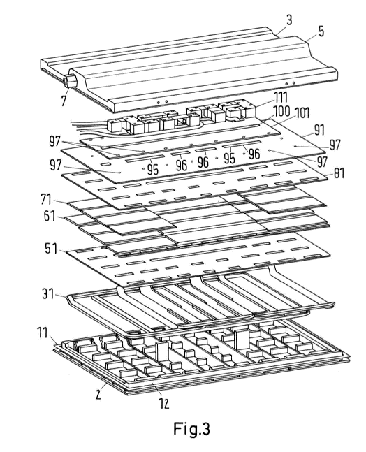
The exploded view of Fig. 3 shows a specific embodiment of a receiving device,
wherein
the components of the receiving device are housed by the case shown in Fig. 1
and Fig 2.
The base part 2 of the case carries a holding device 12 for holding other
interior
components of the receiving device, in particular electric lines that form in
each case two
coils of three phases. In addition, the holding device 12 comprises a
plurality of columns
for separating, holding and/or fixing components of the receiving device which
are located
above the coils. In particular, at least one intermediate layer of insulating
and/or elastic
material, magnetic material, a layer of electrically conducting shield
material and/or a base
plate for an electric circuit arrangement can be separated, held and/or fixed
using one or
more than one of the columns.
When the cover 3 of the case is mounted to the base plate 2 of the case, the
outer rim of
the cover 3 abuts on a sealing 11 which is positioned in the periphery of the
holding
device 12 and is supported by the rim of the base plate 2.
A coil arrangement 31 is positioned within pre-defined receiving spaces of the
holding
device 12. Since the different electric lines (phase lines) for producing the
different phases
of an alternating current form coils which overlap each other if viewed from
the top (from
the cover 3), the phase lines of at least two of the phases rise nearby the
longitudinal
sides of the coil arrangement so that they extend along the longitudinal side
one upon the
other, where they overlap. Details of a specific embodiment of this kind are
shown in Fig.
4 and will be described later.
The coil arrangement 31 is covered by a layer 51 of elastic material which is
preferably
also electrically insulating. The layer 51 may be formed by a single piece of
material or by
a plurality of pieces.
An arrangement 61 of magnetizable material, in particular ferrimagnetic
material or
alternatively ferromagnetic material, is placed on the intermediate layer 51.
Preferably, the
height (i.e. the depth) of the magnetic material differs and is larger above
(i.e. behind)
CA 02899285 2015-07-24
WO 2014/166969 PCT/EP2014/057094
12
regions where the density (number per length) of the electric lines of the
coil arrangement
31 is higher.
Preferably, compensating material 71 is placed where the height of the
magnetic material
61 is smaller so that the height of the total arrangement of magnetic material
61 and
compensating material 71 is constant or, at least, varies less than the height
of the
magnetic material 61.
In the specific embodiment shown in Fig. 3, a second intermediate layer 81,
which may be
have the features described above for the intermediate layer 51, is placed on
top of the
magnetic material 61 or the compensating material 71.
A shielding layer 91 made of electrically conducting material, for example
aluminum, is
placed on top of the second intermediate layer 81. The shielding layer 91 has
cut outs 95
so that at least some of the columns of the holding device 12 can extend
through the cut
outs 95. Some cut outs or regions 96 of the cut outs can be used for placing
sections of
electric connections between the coil arrangement 31 and the electric circuit
111 that is
placed above the shielding layer 91.
The circuit arrangement 111 is placed on a sheet-like carrier 101, such as a
conventional
circuit board. There is a cut out 100 in the carrier 101 so that electric
connections between
the circuit arrangement 111 and the coil arrangement 31 can extend through the
cut out
100.
In the specific embodiment shown in Fig. 3, the carrier 111 and the shielding
layer 91
comprise bores 97 or other cut outs which allow for fixing the carrier 101 to
columns of the
holding device 12 so that the complete arrangement of interior components of
the
receiving device is fixed to the holding device 12. In particular, the
electric circuit
arrangement 111 can be fixed to the carrier, for example by soldering, and the
holding
device 12 can be fixed to the base plate 2 of the case, such as by gluing or
screwing.
Preferably, screws are also used to fix the carrier 101 to the columns of the
holding device
12.
A preferred embodiment of the coil arrangement 31 is shown in Fig. 4. The coil
arrangement consists of six coils 33a, 33b, 35a, 35b, 37a, 37b, two coils per
phase line
CA 02899285 2015-07-24
WO 2014/166969 PCT/EP2014/057094
13
32, 34, 36. The coils of each phase line are placed next to each other on the
same height
level of the receiving device. Fig. 4 shows an exploded view of the coil
arrangement 31.
To form the two coils of one phase, the respective phase line 32, 34, 36 is
wound starting
at one end of a first coil around the area to be covered so as to form the
first coil and
further extends around the area to be covered by the second coils so as to
form the
second coil. In the example shown in Fig. 4, each coil may comprise two to
five windings.
The number of the windings of the phase lines 32, 34, 36 is not shown in the
figures.
As mentioned before, the coils of the different phases overlap each other
partially in the
middle region of the coil arrangement 31. The phase lines 32, 34, 36 are
placed one upon
the other where the coils overlap. Since transversally extending sections of
the different
phase lines 32, 34, 36, which sections connect the longitudinal sides, are
placed on the
same height level in the finished coil arrangement 31, at least the phase
lines 34, 36 rise
along their extension next to the longitudinal sides of the coils. The holding
device 12
defines spaces for receiving these transversely extending sections of the
phase lines,
wherein the spaces are on the same height level.
Although the phase lines 32, 34, 36 are preferably electrically insulated at
their surfaces,
the coils 33, 35, 37 of the different phases are preferably placed upon each
other using
distance pieces 41, 42, 43. These pieces are placed in between the phase lines
32, 34, 36
where they are placed one upon the other. In particular, there are three types
of distance
pieces. The first type 41 is used where the phase line 34 of the second phase
is placed
above the phase line 32 of the first phase along the longitudinal side of the
coil
arrangement 31. The first type 41 of distance pieces is elongated and extends
along the
longitudinal side and, at the same time, along the phase lines 32, 34 so as to
form a
distance between the phase lines 32, 34. The first type 41 of the distance
pieces has a
constant cross section. It is used for the second coil 33b of the first phase.
The second type 42 of distance pieces does not have a constant cross section,
but the
end region shown on the right hand side of Fig. 4 is significantly higher than
the other
sections. Where the distance pieces 42 are higher, the first coil 33a of the
first phase
supports the first coil 37a of the third phase. Where the height of the
distance pieces 42 is
smaller, the first coil 33a of the first phase supports the first coil 35a of
the second phase.
CA 02899285 2015-07-24
WO 2014/166969 PCT/EP2014/057094
14
The third type 43 of the distance pieces also has a non-constant, varying
cross section.
The end regions of the distance pieces 43 are higher than the other regions.
Where the
height is larger, the second coil 35b of the second phase supports other
components of
the receiving device which are placed above the coil arrangement 31. Where the
height of
the distance pieces 43 is smaller, the second coil 35b or the first coil 35a
of the second
phase supports the first or second coil 37a, 37b of the third phase.
In particular, the number of the distance pieces 41, 42, 43 depends on the
number of
windings per coil. Since the number of windings may differ in different
embodiments of the
arrangement, Fig. 4 shows different numbers of the different types of the
distance pieces
41, 42, 43. However, in practice, it is preferred that all coils comprise the
same number of
windings and, consequently, that the numbers of the different types of
distance pieces are
equal.
The longitudinal section of the coil 33b of the first phase is fully
overlapped by the coils
35a, 35b of the second phase. If the coils 35a, 35b are placed on top of the
coils 33a, 33b,
the transversely extending section at the side face of coil 35b is placed
outside of the area
which is covered by the second coil 33b of the first phase. The transversely
extending
section of the second phase which comprises sections of the first coil 35a and
the second
coil 35b is placed in the area around which the phase line 32 of the second
coil 33b of the
first phase extends. The transversely extending section of the first coil 35a
of the second
phase is placed in the area around which the phase line 32 of the first coil
33a of the first
phase extends. The corresponding arrangement can be perceived from Fig. 3: the
transversely extending sections of the coils are separated from the
neighbouring
transversely extending section of another coil in each case by at least one of
the columns.
In the example shown, there are five columns in each case in between two
neighbouring
transversely extending sections.
The coils 35 of the second phase and the coils 37 of the third phase are
shifted in a
similar manner relative to each other as the first phase and the second phase,
but the shift
length in longitudinal direction is twice as large as the shift length of the
first and second
phase. As a result, the transversely extending section at the side face of the
first coil 37a
of the third phase is placed outside of the area around which the phase line
32 of the first
coil 33a of the first phase extends. On the other hand, the shift length in
longitudinal
direction of the third phase relative to the first phase has the same amount
as the shift
CA 02899285 2015-07-24
WO 2014/166969 PCT/EP2014/057094
length of the first phase and the second phase, but is oriented in the
opposite direction if
viewed from the first phase coil arrangement.
At least one end of the phase line 32, 34, 36 which forms the coils of the
respective phase
is connected to a line section or forms a line section that extends upwards
from the coils.
Respective upwardly extending sections 38, 39, 40 are shown in Fig. 4. The
other ends of
the phase lines 32, 34, 36 can directly be connected to each other (not shown
in Fig. 4) so
as to form an electrical star point. Since at least one end of each phase line
32, 34, 36 is
connected to an upwardly extending section 38, 39, 40, the coil arrangement
can be
electrically connected in a different region (in particular on a higher level)
of the receiving
device, in particular to components which are located in the protruding
portion of the case.
In particular, the upwardly extending sections 38, 39, 40 are connected to in
each case at
least one capacitor of the circuit arrangement 111 shown in Fig. 3 and Fig. 9.
The enlarged view of the base plate 2 and the holding device 12 shown in Fig.
5
comprises a plurality of columns 13, 14, 15 which extend upwards from the
basis of the
holding device. A preferred material of the holding device 12 is plastic, such
as a polymer.
Preferably, the basis of the holding device 12 is sheet-like forming a planar
or merely
planar outer surface facing to the base plate 2. Preferably, the columns 13,
14, 15, the
basis and optionally further portions (e.g. holding portions for holding
electric lines or
bundles of electric lines) of the holding device 12 are formed as an integral
part, for
example by injection moulding. Alternatively, at least one of the columns 13,
14, 15 can be
manufactured as a separate piece and can be fixed to the basis.
The holding device 12 comprises holding portions 16, 17 for holding electric
lines or
bundles of electric lines. Depending on the number of the electric lines or
bundles of
electric lines to be held by the individual holding portion 16, 17, the
holding portions are
wider or narrower (with respect to the longitudinal direction). In the example
shown in Fig.
5, the first three holding portions 16 from the left and from the right in the
figure are
narrower than the three holding portions 17 in the middle.
The columns 13, 14, 15 are arranged in lines extending in the longitudinal
direction (from
left to right in Fig. 5) and rows extending in transverse direction (from
front to back in Fig.
5). There are spaces in between the rows of columns and beyond the first and
last row,
wherein these spaces are adapted to receive the respective transversely
extending
CA 02899285 2015-07-24
WO 2014/166969 PCT/EP2014/057094
16
sections of the coils of the coil arrangement, in particular the coil
arrangement 31 as
shown in Fig. 4. In the specific embodiment shown in Fig. 5, the width of
these spaces as
measured in the longitudinal direction differs corresponding to the number of
sections of
electric lines which are to be placed side by side to each other on the same
height level.
Consequently, in view of the coil arrangement 31 shown in Fig. 4, the first
three spaces
have a smaller width which is in particular half as wide as the width of the
three spaces in
the middle of the holding device 12.
The lines of the columns 13, 14, 15 are spaced so that pieces of magnetic
material and
optionally compensating material can be placed in between in each case two of
the
columns.
In addition, at least one of the columns 13, 14, 15 can be used for fixing
other components
of the receiving device to the column and thereby to the holding device 12.
Therefore, the columns combine different functions, in particular separating
different
transversely extending sections of coil, separating different pieces of
material, such as
magnetic material and compensating material, and/or fixing other components to
the
respective column. A further possible function is separating components of the
receiving
device from the basis of the holding device and/or from the basis of the
receiving device at
the receiving side. "Separating" means that the respective components or parts
cannot
contact each other. The respective dimension of the column, either in
longitudinal
direction, in transverse direction or in height direction, defines the minimum
distance
between the two parts or components which are separated.
In addition, as mentioned before, the specific embodiment of the holding
device 12 shown
in Fig. 5 comprises elevated rims 18 along the longitudinal sides. In any
case, the rims of
the holding device along the longitudinal sides are adapted to receive the
corresponding
sections of the coil arrangement.
Preferably, the spaces for receiving the phase lines of the coil arrangement
have shaped
surfaces, in particular grooved surfaces, so that the phase lines are held in
place and do
not slip. In particular, these spaces can be provided by holding portions of
the holding
device.
CA 02899285 2015-07-24
WO 2014/166969 PCT/EP2014/057094
17
In particular, two columns 15 of the holding device 12 are higher than the
other columns
13, 14 and serve to position and/or fix the carrier 101 and the circuit
arrangement 111
shown in Fig. 3 and Fig. 9.
The intermediate layer 51 (and optionally the intermediate layer 71) shown in
Fig. 3 are
shaped as shown in Fig. 6. The layer 51 may be made of an elastic material,
such as
silicone. The layer 51 comprises a plurality of cut outs 23, 24, 25 which are
arranged in
lines and rows similarly to the lines and rows of the columns 13, 14, 15 of
the holding
device 12. Preferably, the cut outs 23, 24, 25 are sized so that the columns
may extend
through the cut outs while abutting to the surfaces of the cut outs 23, 24,
25. It is preferred
that the surfaces of the cut outs 23, 24, abut to the surface of the
respective column 13,
14 all around the column. In the center line of the receiving device and,
therefore, of the
layer 51, there is the cut out 25 which has a length that is larger than the
length of the
columns 15. This allows for passing other components through the cut out 25.
In
particular, the upwardly extending line sections 38, 39, 40 shown in Fig. 4
may extend
through the cut out 25.
Fig. 7 and Fig. 8 schematically show the arrangement of a plurality of
magnetic material
pieces 62 (e.g. pieces having the shape of a cuboid) which is to be placed on
an
intermediate layer 51 which may be the intermediate layer 51 shown in Fig. 6.
However,
the number of cut outs 23, 24 and their shapes may vary from embodiment to
embodiment. In addition, the arrangement can be used with a different type of
receiving
device as described with reference to the figures. Fig. 7 and Fig. 8 show the
principle of
placing magnetic material above the coil arrangement of a receiving device,
independent
of the interior components used in the receiving device and independent of the
specific
dimensions of the interior components of the receiving device.
In Fig. 7, areas 63 where magnetic material pieces 62 are to be placed are
indicated by
dashed outlines. For a first line of such areas 63, the pieces 62 are shown in
the exploded
view of Fig. 7. There are four pieces 62 to be placed on top of the two areas
63 in the
middle of the line and there are only two pieces 62 to be placed on the two
areas 63 at the
end of the line. The resulting stacked arrangement of pieces 62 is
schematically shown in
Fig. 8. Since all pieces 62 have the same dimensions, the two stacks in the
middle are
twice as high as the two stacks at the opposite ends of the line. The
motivation for these
different total heights of magnetic material is the overlap of the different
phase lines 32,
CA 02899285 2015-07-24
WO 2014/166969 PCT/EP2014/057094
18
34, 36 which form the coils of the different phases, for example as shown in
Fig. 4. Higher
magnetic field strengths caused by more electric lines require more magnetic
material.
In order to compensate for the different heights of the magnetic material,
compensating
material 72 is placed as shown in Fig. 8.
Fig. 7 also shows the cut outs 23, 24 and that the lines of areas where the
magnetic
material is to be placed are located in between the lines of the cut outs 23,
24. In
longitudinal direction, it is preferred that the magnetic material pieces 62
abut to each
other (in contrast to the small distances shown in Fig. 8). As preferred, at
least one
column (not shown in Fig. 7) and preferably a plurality of columns extend(s)
in each case
through one of the cut outs 23, 24, thereby separating the lines of the
magnetic material
pieces 62.
Variations of the embodiment of a field shaping arrangement shown in Fig. 7
and Fig. 8
are possible. In particular, it is not necessary to combine the arrangement
with one of the
intermediate layers or any of the intermediate layers shown in Fig. 6.
Furthermore, the
columns can be omitted. In addition, the shape of the elements made of
magnetizable
material may be different. However, shapes are preferred which allow for
producing a
mosaic of elements having seams between the elements, but no other hollow
spaces.
Fig. 9 shows an enlarged view of the carrier 101 and of the electric circuit
arrangement
111 which is carried and preferably fixed on the carrier 101. There is a
plurality of block-
shaped capacitors 115, some of which are electrically connected to each other
by plate-
like electrical connectors 116. In addition, the capacitors 115 are
electrically connected to
the respective coil in particular via the upwardly extending connecting
sections 38, 39, 40
shown in Fig. 4 and are electrically connected via connection lines 112, 113,
114 to an
external device, in particular to the rectifier 120 shown in Fig. 10. These
external
connection lines 112, 113, 114 can be guided through the connecting part 7
shown in
Fig. 1 and Fig. 2.
At least the upper part of the circuit arrangement 111 shown in Fig. 9 can be
placed within
the protruding portion 5 of the cover 3 of the case shown in Fig. 1 and Fig.
10. The
protruding portions 6a, 6b of the cover 3 along the longitudinal sides are
preferably used
CA 02899285 2015-07-24
WO 2014/166969 PCT/EP2014/057094
19
for receiving at least sections of the phase lines and optionally of the
spacing pieces of the
coil arrangement, such as the circuit arrangement 31 shown in Fig. 4.
Fig. 10 shows the receiving device 1 of Fig. 1 and a rectifier 120 which is
housed by a
housing 121. In particular, the connecting lines 112, 113, 114 shown in Fig. 9
connect the
receiving device 1 with the rectifier 120.
The central protruding portion 5 of the receiving device 1 is elongated and
extends along
a longitudinal axis which is also the longitudinal axis of the housing 121 of
the rectifier
120. This arrangement can be placed in corresponding recesses formed by the
bottom
surface of the car body of a road vehicle. Such a road vehicle 141 is shown in
Fig. 11. The
location of the receiving device is schematically indicated by a block with
reference
numeral 143 and the location of the rectifier is schematically indicated by a
block with
reference numeral 144.
During energy transfer to the vehicle, a generating device 142 generates the
magnetic
field, in particular by generating an alternating electromagnetic field. The
magnetic field is
indicated by three curved lines. The generating device 142 is provided with
electric current
from corresponding equipment 145, which may include an inverter and/or an
AC/AC
converter.
Figure 12 shows five columns 13, 15 which extend upwards from a base plate of
a
separating structure 12, wherein the receiving side of the receiving device is
at the bottom
of the figure. A layer 51 of elastic material extends at a distance and
parallel to the base
plate. In a similar manner as shown in the exploded view of Fig. 8, pieces of
magnetic
material 62 are laid on the layer 51 in between the columns 13, 15.
Consequently, the
columns 13, 15 separate the pieces of magnetic material 62. In addition, the
columns 13,
15 extend through cut outs of the layer 51.
Figure 13 shows three columns 13, 14, 15 which extend upwards from a base
plate of a
separating structure 12, wherein the receiving side of the receiving device is
at the bottom
of the figure. In the same manner as shown in figure 12, the layer 51 of
elastic material
extends at a distance and parallel to the base plate. While Fig. 12 shows a
region of the
arrangement where no electric lines of the coil arrangement are positioned in
between the
base plate and the layer 51, Fig. 13 shows a region of the arrangement where
bundles of
CA 02899285 2015-07-24
WO 2014/166969 PCT/EP2014/057094
electric lines, in particular the phase lines 34, 36 of the arrangement shown
in Fig. 4, of
the coil arrangement are positioned in between the base plate and the layer
51. The
bundles are held by holding portions 16, 17 of the separating structure 12.
The holding
portions 16, 17 in each case form a groove for receiving the electric lines
34, 36. In case
of the receiving portions 16, there are three electric lines 36 side-by-side
in the groove. In
case of the receiving portions 17, there are five electric lines 34 side-by-
side in the
groove. In alternative embodiments, the electric lines may be held in a
different manner,
for example using a groove for each single electric line and/or with electric
lines not or not
only side-by-side in the longitudinal direction (horizontal direction in Fig.
13), but stacked.
Consequently, the column 15 separates the holding portions 16, 17 and thereby
the
bundles of electric lines 34, 36. In addition, the column 15 extends through a
cut out of the
layer 51.
Modifications of the arrangement shown in Fig. 12 and Fig. 13 are possible.
For example,
the numbers and/or dimensions of the elements and components shown in the
figures
may vary. In addition, the columns may be used for separating, holding and/or
fixing other
components of the receiving device in addition to the components shown in the
figures or
alternatively to the at least a part of the components shown in the figures.