Note: Descriptions are shown in the official language in which they were submitted.
MINIATURE SENSOR STRUCTURES FOR ION MOBILITY
SPECTROMETERS
RELATED APPLICATIONS
This application claims priority to U.S. Provisional App. No. 61/769,320,
filed
February 26, 2013, entitled "Making Miniature Drift Tubes for Ion Mobility
Spectrometers."
TECHNICAL FIELD
This application is related to the field of chemical analysis and, in
particular, ion
mobility spectrometry.
BACKGROUND OF THE INVENTION
Ion mobility spectrometry (IMS) utilizes relative low electric fields to
propel
ions through a drift gas chamber and separate these ions according to their
drift
velocity. In IMS, the ion drift velocity is proportional to the field strength
and thus an
ion's mobility (K) is independent of the applied field. In the IMS both
analyte and
background molecules are typically ionized using radioactive alpha or beta
emitters and
the ions are injected into a drift tube with a constant low electric field
(300 V/cm or
less) where they are separated on the basis of their drift velocity and hence
their
mobility. The mobility is governed by the ion collisions with the drift gas
molecules
flowing in the opposite direction. The ion-molecule collision cross section
depends on
the size, the shape, the charge, and the mass of the ion relative to the mass
of the drift
gas molecule. The resulting chromatogram is compared to a library of known
patterns to
1
Date Recue/Date Received 2020-05-27
identify the substance collected. Since the collision cross section depends on
more than
one ion characteristic, peak identification is not unique. IMS systems measure
a
secondary and less specific property of the target molecule-the time it takes
for the
ionized molecule to drift through a tube filled with a viscous gas under an
electric field-
and the identity of the molecule is inferred from the intensity vs time
spectrum.
Other mobility-based separation techniques include high-field asymmetric
waveform ion mobility spectrometry (FAIMS) also known as Differential Mobility
Spectrometry (DMS). FAIMS or DMS is a detection technology which can operate
at
atmospheric pressure to separate and detect ions. Compared to conventional ion
mobility, FAIMS/DMS devices operate at much higher fields (-10,000 V/cm) where
ion mobilities become dependent on the applied field. FAIMS/DMS devices may
operate in conjunction with IMS drift tube devices in spectrometers having
multiple
stages. For specific descriptions of features and uses of instruments for ion
detection
and chemical analysis, including features of IMS drift tube devices used in
connection
with one or more FAIMS/DMS devices, among other components, reference is made
to
US. Patent No. 8,173,959 B1 to Boumsellek et al., entitled "Real-Time Trace
Detection
by High Field and Low Field Ion Mobility and Mass Spectrometry," U.S. Pub. No.
2012/0273669 Al to Ivashin et al., entitled "Chemical Analysis Using
Hyphenated Low
and High Field Ion Mobility," and U.S. Pub. No. 2012/0326020 Al to Ivashin et
al.,
entitled "Ion Mobility Spectrometer Device with Embedded FAIMS."
Known IMS device construction techniques include the use of alternate stacking
of metallic and insulator rings to produce sensor structures. These sensors
structures,
such as IMS drift tubes, are used in the ion transport and analysis
applications at
atmospheric or near atmospheric pressure. Further, other techniques are known
for
producing IMS sensor structures using ceramic material rolling processes. For
example,
U.S. Patent No. 7,155,812 B1 to Peterson et al., entitled "Method for
Producing a
Tube," discloses a process of rolling a pliable green (i.e. prefired) ceramic
sheet around
2
Date Recue/Date Received 2020-05-27
a form for multiple revolutions and in which electrical conductors are
disposed on a
surface of the ceramic sheet. The rolled ceramic sheet is subject to pressure
and fired to
produce the IMS drift tube. The ceramic may be a low temperature co-fired
ceramic
(LTCC). It is noted that in some cases use of a continuously rolled sheet
process may
limit the functionality and complexity of circuit or sensor components of the
IMS drift
tube. Other techniques for producing three-dimensional ceramic circuit
structures are
described in U.S. Patent No. 6,527,890 to Briscoe et al., U.S. Patent No.
5,028,473 to
Vitriol et al., U.S. Patent No. 4,475,967 to Kanai et al., and U.S. Patent No.
3,755,891
to Muckelroy et al.
Accordingly, it would be desirable to provide advantageous and efficient
techniques for producing high performance, low cost, miniature drift tubes or
other
sensor structures for IMS devices on a large production scale.
SUMMARY OF THE INVENTION
According to the system described herein, a method for making a sensor
structure includes forming a shaped structure made of a high temperature, non-
electrically-conductive ceramic material. At least one via hole is formed in
the shaped
structure. Circuitry features are formed on the shaped structure. The shaped
structure is
processed to obtain a sensor structure. The ceramic material may be aluminum
nitride or
alumina, and the sensor structure may be an ion mobility spectrometry drift
tube.
Forming the shaped structure may include applying and forming at least two
discrete
sheets of the high temperature, non-electrically-conductive ceramic material
into a
structure having a desired shape, and the at least one via hole in the shaped
structure
may be formed to provide a via hole that connects the interior and exterior of
the shaped
structure. Forming the shaped structure may include preforming a solid tube of
the high
temperature, non-electrically-conductive ceramic material, and the at least
one via hole
may be machined into the solid tube.
3
Date Recue/Date Received 2020-05-27
CA 02901002 2015-08-11
WO 2014/134156 PCT/US2014/018648
Forming the circuitry features may include forming conductive or resistive
features on the shaped
structure using an ink deposition process.
According further to the system described herein, a sensor structure includes
a shaped
structure made of a high temperature, non-electrically-conductive ceramic
material. Circuitry
features are formed on the shaped structure. At least one via hole is formed
in the shaped structure.
The ceramic material may be aluminum nitride or alumina, and the sensor
structure may be an ion
mobility spectrometry drift tube. The shaped structure may be formed from
applying and forming
at least two discrete sheets of the high temperature, non-electrically-
conductive ceramic material
into a structure having a desired shape, and the at least one via hole in the
shaped structure may be
formed to provide a via hole that connects the interior and exterior of the
shaped structure. The
shaped structure may include a preformed solid tube of the high temperature,
non-electrically-
conductive ceramic material, and the at least one via hole may be machined
into the solid tube. The
circuitry features may include be formed by forming conductive or resistive
features on the shaped
structure using an ink deposition process.
According further to the system described herein, an ion mobility spectrometer
device
includes an ion source, an analyzer component, and a drift tube coupled
between the ion source and
the analyzer component. The drift tube includes a shaped structure made of a
high temperature,
non-electrically-conductive ceramic material. Circuitry features are formed on
the shaped structure.
At least one via hole is formed in the shaped structure. The ceramic material
may be aluminum
nitride or alumina, and the sensor structure may be an ion mobility
spectrometry drift tube. The
shaped structure may be formed from applying and forming at least two discrete
sheets of the high
temperature, non-electrically-conductive ceramic material into a structure
having a desired shape,
and the at least one via hole in the shaped structure may be formed to provide
a via hole that
4
CA 02901002 2015-08-11
WO 2014/134156 PCT/US2014/018648
connects the interior and exterior of the shaped structure. The shaped
structure may include a
preformed solid tube of the high temperature, non-electrically-conductive
ceramic material, and the
at least one via hole may be machined into the solid tube. The circuitry
features may include be
formed by deposited conductive or resistive features that are deposited on the
shaped structure using
an ink deposition process.
BRIEF DESCRIPTION OF THE DRAWINGS
Embodiments of the system described herein are explained with reference to the
several
figures of the drawings, which are briefly described as follows.
FIG. 1 is a schematic illustration showing an individual ceramic sheet that
may be used in
connection with making high performance, low cost, miniature sensors
structures on a large
production scale using ceramic materials according to the embodiment of the
system described
herein.
FIG. 2 is a schematic illustration showing an end view of multiple ceramic
sheets that have
been layered over one another around a shape, such as a cylindrical mandrel in
connection with
producing an IMS sensor structure, such as an IMS drift tube.
FIG. 3 is a schematic illustration showing an end view for another embodiment,
as
compared to FIG. 2, in which multiple ceramic sheets have been layered over
one another around a
shape, such as a cylindrical mandrel in connection with producing an IMS
sensor structure, such as
an IMS drift tube.
5
CA 02901002 2015-08-11
WO 2014/134156 PCT/US2014/018648
FIGS. 4A and 4B are schematic illustrations showing an alternative
construction for an IMS
drift tube according to an embodiment of the system described herein.
FIG. 5 is a schematic illustration showing an IMS drift tube produced
according to an
embodiment of the system described herein.
FIG. 6 is schematic perspective illustration showing an example IMS device
produced
according to an embodiment of the system described herein.
FIG. 7 is a flow diagram showing processing for making a sensor structure
according to an
embodiment of the system described herein.
FIG. 8 is a flow diagram showing processing for making a sensor structure
according to
another embodiment of the system described herein.
DETAILED DESCRIPTION OF VARIOUS EMBODIMENTS
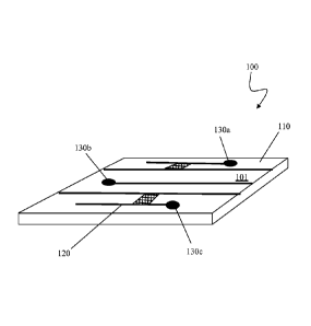
FIG. 1 is a schematic illustration 100 showing an individual ceramic sheet 101
that may be
used in connection with making high performance, low cost, miniature sensors
structures on a large
production scale using ceramic materials according to the embodiment of the
system described
herein. The sensor structure may be created in part or in whole from multiple
discrete individual
sheets, like the sheet 101, that may be flat pliable sheets of green-state
ceramic material 110. In
various embodiments, the sensor structure may, for example, be an ion guide
and/or an IMS drift
tube, as further discussed elsewhere herein.
6
CA 02901002 2015-08-11
WO 2014/134156 PCT/US2014/018648
In an embodiment, the ceramic material 110 may be aluminum nitride, alumina
and/or other
high temperature non-electrically conductive material. In particular, aluminum
nitride has an
advantageously high thermal conductivity, for example up to one hundred times
greater than the
thermal conductivity of low temperature co-fired ceramic (LTCC), and thereby
may be beneficially
used in IMS drift tubes or other sensor structures since the use of aluminum
nitride allows IMS
device products to come up to temperature faster. Further use of aluminum
nitride mitigates and/or
eliminates cold spots which, if present, lead to extended clear down times
after the introduction of a
sample into the drift tube.
A desired shape of each sensor structure may be created by applying, forming
and joining
the individual sheets into the desired shape, for example, by applying the
sheets as layers around
either a male or female form tool such as a cylindrical mandrel or other
shape, as further discussed
elsewhere herein. During the green state of the sheet(s) 101, conductive
features 120, such as
discrete or continuous metal surfaces, may be placed on the individual ceramic
sheet 101 by screen
printing or other deposition methods. The features 120 may serve as
electrodes establishing
electrostatic fields to control ion motion, current-based heaters, electronic
shields, bonding surfaces
for secondary attachment, and/or other appropriate circuitry structure or
other sensor features. In
various embodiments, the layers may have the features 120 on one surface of
the sheet 101, both
surfaces and/or neither surface as needed or desirable to create a required
circuit structure. One or
more via holes 130a, 130b, 130c may also be formed into the sheet 101, as
further discussed
elsewhere herein.
FIG. 2 is a schematic illustration 200 showing an end view of multiple ceramic
sheets 201,
202, 203 that have been layered over one another around a shape, such as a
cylindrical mandrel in
connection with producing an IMS sensor structure, such as an IMS drift tube.
Each of the ceramic
7
CA 02901002 2015-08-11
WO 2014/134156 PCT/US2014/018648
sheets 201, 202, 203 may be like the described ceramic sheet of FIG. 1 but
having particular
conductive and circuitry features as required to create the desired circuitry
configuration of the IMS
drift tube. Although three sheets 201-203 are illustrated, any appropriate
number of sheets may be
used for a desired structure. According to the system described herein, the
design and layering of
.. the ceramic sheets 201, 202, 203 may be such that each sheet, when formed
into the desired shape,
is positioned according to desired circuitry configurations. For example, the
ceramic sheets 201,
202, 203 may be designed, when layered, to be applied such that abutting ends
of the ends
positioned along a single seam for desired circuitry configurations. The
sheets 201, 202, 203 may
each contain one or more via holes 211, 212, 213. The via holes 211, 212, 213
may be provided at
.. locations that facilitate subsequent electrical connections among the
layers 201, 202, 203 to form
the desired circuit structure. For example, in the illustrated embodiment
shown in FIG. 2, the via
holes 211, 212, 213 provided in each of the sheets may form one or more via
holes through from the
inside of the drift region of the IMS drift tube to the outside of the IMS
device. Each of the
ceramic sheets 201, 202, 203 may be made of aluminum nitride, alumina and/or
other high
temperature non-electrically conductive material. The via holes 211, 212, 213
may be metallized,
as further discussed herein, and may include use of contact pads to enable
electrical connections
between circuitry features of the sheets 201, 202, 203 according to various
embodiments of the
system described herein. The structure may be subject to a high pressure and
temperature
environment to produce a fused monolithic sensor structure, such as an IMS
drift tube.
FIG. 3 is a schematic illustration 300 showing an end view for another
embodiment, as
compared to FIG. 2, in which multiple ceramic sheets 301, 302, 303 have been
layered over one
another around a shape, such as a cylindrical mandrel in connection with
producing an IMS sensor
structure, such as an IMS drift tube. In the illustrated embodiment, the via
holes 311, 312, 313
.. formed are staggered throughout the width of the IMS drift tube. The
staggering of the via holes
8
CA 02901002 2015-08-11
WO 2014/134156 PCT/US2014/018648
311, 312, 313 may be to provide the suitable circuitry configuration of the
1MS drift tube. Each of
the ceramic sheets 301, 302, 303 may be made of aluminum nitride, alumina
and/or other high
temperature non-electrically conductive material. It is further noted that the
sheets 301, 302, 303
themselves, may be layered such that abutting ends of the sheets, after
application of the sheets, are
staggered around the circumference of the drift tube in accordance with
designed circuitry
configurations of circuitry features on the sheets 301, 302, 303 that may be
electrically connected
using the via holes 311, 312, 313. It is also noted that various combinations
of the embodiments
described in connection with FIGS. 2 and 3 may be appropriately used according
to the system
described herein.
FIGS. 4A and 4B are schematic illustrations 400, 400' showing an alternative
construction
for an IMS drift tube according to an embodiment of the system described
herein. FIG. 4A is a
schematic illustration of a solid tube 410 that, in the alternative
construction technique, may be pre-
formed from a high temperature non-electrically conductive material, such as
alumina or, in
particular, aluminum nitride. FIG. 4B is schematic illustration of an end view
of the solid tube 410.
One or more via holes 411, 412, 413 may be drilled or otherwise machined
through the sheet 101 at
predetermined locations to facilitate subsequent electrical connections from
the inside of the drift
region of the tube 410 to the outside. The inside drift region may be
metallized with a layer 420,
such as by a metallic ink deposition process, to support the creation of
electrode rings of the tube
410. In an embodiment, the metallization may be through the use of thick film
metallization, and
the via holes 411-413, with associated connection pads, may also be metallized
so as to electrically
connect from the metallized surface of the interior drift region to the
exterior of the IMS device. It
should also be noted that, in addition to the via holes 411-413, electrical
connections may be
accomplished by adding traces along the surfaces and edges of the ceramic
material. As further
described elsewhere herein, the exterior of the device may also be metallized
to form electrical
9
CA 02901002 2015-08-11
WO 2014/134156 PCT/US2014/018648
traces, shielding, or heater circuits and/or other features in accordance with
the discussion herein.
The metallization may be accomplished using different metals so as to mate the
needs of the surface
with the application. For example, the metal on the drift region may be
selected for low chemical
reactivity while the metal in the via and associated pads may be selected to
support secondary
operations such as filling, brazing or soldering.
Because the metallization process may be imprecise, secondary machining may be
provided,
where necessary, for configuration of the sensor structure in order to remove
any undesired
metallization and restore electrical isolation between metallized regions
inside and outside of the
device. In an IMS configuration, the remaining metallization inside the drift
region may take the
form of separated concentric rings each connected by one or more of the
metallized via holes.
Hermetic sealing of the via holes may be accomplished by any number of
standard methods
including but not limited to soldering, brazing of filler preforms, glass
sealing, adhesives etc. The
tube 410 may be enclosed by attaching drift region cap structures of an IMS
device, as further
discussed elsewhere herein. The cap structures may be attached mechanically to
facilitate
disassembly or more permanently by soldering, brazing of preforms, glass
sealing, adhesives etc.
Additionally and/or alternatively, in other embodiments, more precise methods
of metallic
ink deposition may be used that may avoid the need for secondary machining
noted above. For
example, technology is known that enables use of computer numerical control
(CNC) controlled ink
deposition tips that allow the depositing either resistive and/or conductive
inks onto either the inside
or outside of a curved surface. Reference is made to techniques and products
of Ohmcraft, a
division of Micropen Technologies Corporation. Such products and techniques
may be used to
produce resistive and conductive elements on the interior and exterior of a
drift tube made of
alumina, aluminum nitride or other high temp electrically insulating material,
according to an
embodiment of the system described herein. Reference is made, for example, to
U.S.
Patent No. 7,224,258 B2 to Barge et al., entitled" Fine Line Thick Film
Resistors by
Photolithography," U.S. Patent No. 7,736,592 B2 to Grande et al., entitled
"Microfluidic
Devices Fabricated by Direct Thick Film Writing and Methods thereof," and U.S.
Patent
No. 8,479,585 B2 to Shaw-Klein, entitled " Full-Text Pressure Sensing or Force
Generating Device."
FIG. 5 is a schematic illustration showing an IMS drift tube 500 produced
according to an embodiment of the system described herein. The tube shape of
the drift
tube 500 may be formed by a high temperature electrically-insulating ceramic
material
510, such aluminum nitride and/or alumina. Electrical components and structure
520 may
be formed on the outer surface of the drift tube 500, such as a resistive
heater trace.
Conductive traces 530a-d leading from pads and via holes to connection points
may also
be formed. Inside components 540 may be formed and provided for the drift
region of the
tube 500. For example, in various embodiments, the inside components 540 may
be
electrode rings formed from a deposition method and/or may, for example, be a
continuous
spiral of resistive ink that may be used to replace discrete electrodes and an
external
resistor network.
FIG. 6 is schematic perspective illustration showing an example IMS device 600
produced according to an embodiment of the system described herein. The device
600 may
include an ionizer/ion source 610, a ceramic IMS drift tube 620, and an
analyzer
component 630, such as a detector and/or other component such one or more
additional
analytical component, for example a FAIMS/DMS component, as appropriate or
desirable
for the IMS analysis being performed. The ionizer/ion source 610 may provide a
continuous or a pulsed ion current depending on an operational mode. In an
embodiment,
the ionizer/ion source 610 may include a pulsed ion source,
11
Date Recue/Date Received 2020-05-27
CA 02901002 2015-08-11
WO 2014/134156 PCT/US2014/018648
such as a spark ion source, that may send either individual packets of ions or
a continuous flow of
ions by varying the frequency. Additionally or alternatively, a continuous ion
source may be used
including a DC corona or a radioactive source via an ion gate placed at the
entrance of the IMS drift
tube 620. The IMS drift tube 620 may be formed by using ceramic material, as
according to the
embodiments discussed elsewhere herein, that may include circuitry and
electrical features
necessary to form the drift tube 620.
The system described herein offers multiple advantages in the production of
sensor
structures (e.g. drift tubes) for IMS devices. In particular, manufacturing
costs are significantly
reduced by a reduction in discrete components. Construction may include use of
inert materials
capable of high temperature operation. The use of ceramic materials, such as
aluminum nitride,
provides thermal conductivity of aluminum while maintaining electrical
isolation, and which
supports fast and even heating. Higher density of electrodes is provided using
small width traces
required for miniature drift tubes. Superior inherent hermeticity is provided
by a reduction in the
number of sealing joints and overall sealing length. The concept is scalable
to support different
sized drift regions. Metallization enables multiple functional and
connectivity elements in a single
part.
The method and choice of materials according to the system described herein
further
provides performance advantages. In particular, improved system reliability is
provided through
simplified and flexible designs. Improved resolving power is provided through
the use of high
density electrodes. Extended range of detectable chemical compounds is
provided through rapid
thermal cycling. There is a lack of contamination and better moisture control
through the use of
hermetic tubes. Rapid thermal cycling over a wide range of temperature
settings is enabled by the
12
CA 02901002 2015-08-11
WO 2014/134156 PCT/US2014/018648
use of intimate heater elements. Reduced chemical noise is provided by the
elimination of
polymeric materials frequently required in conventional sensor construction.
FIG. 7 is a flow diagram 700 showing processing for making a sensor structure
according to
an embodiment of the system described herein. At a step 702, one or more
discrete sheets of green-
state ceramic material are produced. In various embodiments, the ceramic
material may be
aluminum nitride, alumina and/or other high temperature, non-electrically-
conductive ceramic
material. The discrete ceramic sheets may be flexibly manufactured and sized
for a desired
application and configuration of an IMS device. After the step 702, at a step
704, circuitry features
are formed into the discrete ceramic sheets for the desired IMS sensor
structure, and including the
formation of via holes in the sheets at desired locations. As further
discussed elsewhere herein, the
circuitry features may be applied by screen printing or other deposition
methods.
After the step 704, at a step 706, the discrete ceramic sheets with deposited
conductive
features are formed into a desired shape, such as by applying the sheets
around a cylindrical
mandrel. In various embodiments, after applying the sheets, the via holes may
be staggered through
the thickness of the tube so as to enable appropriate circuitry configurations
and/or the via holes in
the sheets may aligned co-linearly in connection with the sheet layering to
produce a via hole
through from the interior to the exterior of the tube. After the step 706, at
a step 708, the structure
is subject to a high pressure and temperature environment to produce a fused
monolithic sensor
structure, such as an IMS drift tube. After the step 708, at a step 710, the
sensor structure may be
used in constructing an IMS device, such as by attaching appropriate cap
structures to an IMS drift
tube suitable for an IMS device and operation thereof. After the step 710,
processing is complete.
13
CA 02901002 2015-08-11
WO 2014/134156 PCT/US2014/018648
FIG. 8 is a flow diagram 800 showing processing for making a sensor structure
according to
another embodiment of the system described herein. At a step 802, a preformed
shape, such as a
tube, of ceramic material is produced. In various embodiments, the ceramic
material may be
aluminum nitride, alumina and/or other high temperature, non-electrically-
conductive ceramic
material. After the step 802, at a step 804, at least one via hole is formed
into the ceramic tube from
the structure. The at least one via hole is formed from the exterior to the
interior of the tube. After
the step 804, at a step 806, circuitry features are formed onto the tube. The
circuitry features may
include features formed on the interior and exterior of the tube. It is noted
that the ordering of steps
804 and 806 may be interchanged as appropriate. In an embodiment, the features
may be formed by
a metallization process. For example, the interior of the tube may be
metallized in order to
produce electrode rings of the drift region of the tube. A secondary operation
may be performed
thereafter in order to make the circuitry features more precise and remove
undesired metallization
and/or restore electrical isolation between metallized regions. In other
embodiments, a deposition
process may be used that may avoid the need for secondary machining noted
above. For example,
as discussed elsewhere herein, technology is known that enables use of CNC
controlled ink
deposition tips that allow the depositing of either resistive and/or
conductive inks onto either the
inside or outside of a curved surface using an ink deposition process.
After the step 806, at a step 808, the structure may be subject to any
additional processing to
finalize the circuitry, such as by a firing of deposited inks, where required
in order to produce a
sensor structure, such as an IMS drift tube. After the step 808, at a step
810, the sensor structure
may be used in constructing an IMS device, such as by attaching appropriate
cap structures to an
IMS drift tube suitable for an IMS device and operation thereof. After the
step 810, processing is
complete.
14
CA 02901002 2015-08-11
WO 2014/134156 PCT/US2014/018648
Various embodiments discussed herein may be combined with each other in
appropriate
combinations in connection with the system described herein. Additionally, in
some instances, the
order of steps in the flowcharts, flow diagrams and/or described flow
processing may be modified,
where appropriate. Further, various aspects of the system described herein may
be implemented
using software, hardware, a combination of software and hardware and/or other
computer-
implemented modules or devices having the described features and performing
the described
functions. The system may further include a display and/or other computer
components for
providing a suitable interface with a user and/or other computers.
In connection with applicable control processing, software implementations of
the system
described herein may include executable code that is stored in a computer-
readable medium and
executed by one or more processors. The computer-readable medium may include
volatile memory
and/or non-volatile memory, and may include, for example, a computer hard
drive, ROM, RAM,
flash memory, portable computer storage media such as a CD-ROM, a DVD-ROM, a
flash drive or
other drive with, for example, a universal serial bus (USB) interface, and/or
any other appropriate
tangible or non-transitory computer-readable medium or computer memory on
which executable
code may be stored and executed by a processor. The system described herein
may be used in
connection with any appropriate operating system.
Other embodiments of the invention will be apparent to those skilled in the
art from a
consideration of the specification or practice of the invention disclosed
herein. It is intended that
the specification and examples be considered as exemplary only, with the true
scope and spirit of
the invention being indicated by the following claims.