Note: Descriptions are shown in the official language in which they were submitted.
INDUCTIVE POWER TRANSMISSION FOR ELECTRICAL DEVICES
CROSS-REFERENCE TO RELATED APPLICATIONS
[0001] Not applicable.
TECHNICAL FIELD
[0002] Embodiments described herein relate generally to inductive power
transmission,
and more particularly to systems, methods, and devices for enabling inductive
power
transmission with electrical devices.
BACKGROUND
[0003] A number of electrical devices, particularly electrical devices used
in
commercial and industrial applications, receive power from sources through
conductors.
Specifically, conductors are electrically and mechanically coupled to a power
source at one end
and the electrical device at the other end. In such a case, a number of
problems can arise at the
connection point between the conductor and the electrical device. For example,
the termination
point between the conductor and the electrical device can overheat, causing
damage to the
conductor, the electrical device, and/or any nearby equipment.
[0004] A termination point between the conductor and the electrical device
can
overheat even more when the termination point becomes loose. Thermal cycling
of the
termination can cause the termination to loosen. In addition, or in the
alternative, a loose
termination point can be caused by one or more of a number of other factors,
including but not
limited to inadequate tightening and vibrations. Other conditions can also
cause overheating of
a termination. For example, corrosion of the termination can increase the
contact resistance of
the termination. As a result, the termination, even if tightly connected, can
overheat. A loose
termination point, corrosion, and/or other conditions that cause overheating
can cause any of a
number of fault conditions. For example, a loose termination can lead to
arcing of electric
current, which can lead to an explosion. If an explosion occurs, the safety of
1
2924519
CA 2903049 2019-02-25
CA 02903049 2015-08-27
WO 2014/137816
PCT/US2014/019472
personnel and equipment can be compromised, even if the explosion occurs in an
electrical enclosure.
SUMMARY
[0005] In general, in one aspect, the disclosure relates to an electrical
system.
The electrical system can include an enclosure, and a power source located
outside the
enclosure and generating a first current. The electrical system can also
include a
transmitting inductor located within the enclosure and electrically connected
to the
power source, where the first current generated by the power source flows
through the
transmitting inductor. The electrical system can further include a receiving
inductor
positioned proximate to the transmitting inductor within the enclosure, where
the first
current flowing through the transmitting inductor induces a second current to
flow
through the receiving inductor. The electrical system can also include a
device
located within the enclosure and electrically connected to the receiving
inductor,
where the second current induced in the receiving conductor powers the device.
[0006] In another aspect, the disclosure can generally relate to an
inductive
power source. The inductive power source can include a cable having a
conductor
disposed within an insulating member. The inductive power source can also
include a
housing disposed on an outer surface of the insulating member. The housing of
the
inductive power source can include a receiving inductor disposed within the
housing,
and an encroacher positioned on a bottom side of the housing and having a
leading
edge that penetrates the insulating member. The housing of the inductive power
source can also include a coupling feature disposed on an outer surface of the
housing. The inductive power source can further include a latch assembly
movably
coupled to the housing. The latch assembly can include an arm that extends
from the
housing, and a harness that couples to the insulating member of the cable. The
latch
assembly can also include a latch that mechanically couples to the coupling
feature of
the housing.
[0007] In yet another aspect, the disclosure can generally relate to an
electrical
connector having a first connector end and a second connector end mechanically
coupled to the first connector end. The first connector end can include a
first sleeve
that forms a first cavity, and a first insulator disposed within the first
cavity. The first
connector end can also include at least one first conductor positioned within
the first
2
CA 02903049 2015-08-27
WO 2014/137816
PCT/US2014/019472
insulator, and at least one transmitting inductor coupled to a distal end of
the at least
one first conductor, where the at least one transmitting inductor is
positioned
proximate to a first open end of the first sleeve. The second connector end
can
include a second sleeve that forms a second cavity, and a second insulator
disposed
within the second cavity. The second connector end can also include at least
one
conductor positioned within the second insulator, and at least one receiving
inductor
coupled to a distal end of the at least one second conductor, where the at
least one
receiving inductor is positioned proximate to a second open end of the second
sleeve.
The first open end and the second open end can abut against each other when
the first
connector end is mechanically coupled to the second connector end.
[0008] These and other aspects, objects, features, and embodiments will be
apparent from the following description and the appended claims.
BRIEF DESCRIPTION OF THE DRAWINGS
[0009] The drawings illustrate only exemplary embodiments of inductive
power transmission and are therefore not to be considered limiting of its
scope, as
inductive power transmission may admit to other equally effective embodiments.
The
elements and features shown in the drawings are not necessarily to scale,
emphasis
instead being placed upon clearly illustrating the principles of the exemplary
embodiments. Additionally, certain dimensions or positionings may be
exaggerated
to help visually convey such principles. In the drawings, reference numerals
designate like or corresponding, but not necessarily identical, elements.
[0010] Figure 1 shows a basic circuit for inductive power transmission.
[0011] Figure 2 shows a schematic view of a system of electrical devices
within an electrical enclosure and receiving inductive power in accordance
with
certain example embodiments.
[0012] Figure 3 shows a schematic view of a system of lighting devices
receiving inductive power in accordance with certain example embodiments.
[0013] Figures 4A and 4B show various views of a system using an inductive
device in accordance with certain example embodiments.
[0014] Figure 5 shows an electrical connector using inductive power
transmission in accordance with certain example embodiments.
3
WO 2014/137816
PCT/US2014/019472
DETAILED DESCRIPTION OF EXAMPLE EMBODIMENTS
[0015] The example embodiments discussed herein are directed to
systems,
apparatuses, and methods of inductive power transmission for electrical
devices. The
electrical devices (or more simply called "devices") can be any devices that
can
receive power from a power source through a conductor and use such power to
operate. In certain example embodiments, the electrical devices are
substantially
fixed in a position and/or within an enclosure. Examples of electrical devices
can
include, but are not limited to, a lighting device, a motor starter switch, a
breaker, a
variable frequency drive (VFD), and a programmable logic controller (PLC). In
some
cases, a number of electrical devices can be electrically connected to each
other in
series and/or in parallel. Such electrical devices can be stand-alone or can
be
positioned within an electrical enclosure.
100161 Such electrical devices may be required to follow certain
standards
and/or regulations that address safety and/or reliability issues. For example,
if the
electrical devices are positioned within a hazardous location enclosure, the
National
Electrical Manufacturers Association (NEMA) sets standards with which an
enclosure must comply in order to qualify as an explosion-proof enclosure.
Specifically, NEMA Type 7, Type 8, Type 9, and Type 10 enclosures set
standards
with which an explosion-proof enclosure within a hazardous location must
comply.
For example, a NEMA Type 7 standard applies to enclosures constructed for
indoor
use in certain hazardous locations. Hazardous locations may be defined by one
or
more of a number of authorities, including but not limited to the National
Electric
Code (e.g., Class 1, Division I) and Underwriters' Laboratories, Inc. (UL)
(e.g., UL
1203). For example, a Class 1 hazardous area under the National Electric Code
is an
area in which flammable gases or vapors may be present in the air in
sufficient
quantities to be explosive.
[0017] As a specific example, NEMA standards for an explosion-proof
enclosure of a certain size or range of sizes may require that in a Group B,
Division
1 area, any flame path of an explosion-proof enclosure must be at least 1 inch
long
(continuous and without interruption), and the gap between the surfaces cannot
exceed 0.0015 inches. Standards created and maintained by NEMA may be found at
www.nema.org/stds. While this example embodiment of inductive power
transmission is directed to an explosion-proof enclosure, example inductive
power
transmission systems can also be used for other
4
Date Recue/Date Received 2020-08-11
CA 02903049 2015-08-27
WO 2014/137816
PCT/US2014/019472
types of enclosures, including but not limited to non-explosion-proof
enclosures,
conduits, light fixtures, and cables. Therefore, example inductive power
transmission
systems described herein should not be considered limited to explosion-proof
enclosures.
[0018] Figure 1 shows a basic circuit 100 for inductive power
transmission.
In one or more embodiments, one or more of the components shown in Figure 1
may
be omitted, repeated, and/or substituted. Accordingly, embodiments of
inductive
power transmission should not be considered limited to the specific
arrangements of
components shown in Figure 1.
[0019] Referring to Figure 1, the left half of the circuit 100 can be
called the
primary portion 101 of the inductive power transmission and can include a
power
source 110, a capacitor 114, a resistor 116, and an inductor 120. One or more
of these
components can be electrically connected to each other using one or more
conductors
112. In this case, the power source 110, the capacitor 114, the resistor 116,
and the
inductor 120 are electrically connected to each other in series in a closed
loop using
the conductors 112.
[0020] In addition, or in the alternative, one or more of one or more
other
electrical components (e.g., a diode, a transistor) can be electrically
connected, in
series and/or in parallel, with one or more components of the primary portion
101 of
the circuit 100. Alternatively, the primary portion 101 of the circuit 100 can
include
only the power source 110 electrically connected to the inductor 120 in
series. In
certain example embodiments, the primary portion 101 includes a number of
inductors (e.g., inductor 120) that are electrically connected in series
and/or in parallel
with each other.
[0021] The right half of the circuit 100 can be called the secondary
portion
102 and can include an inductor 130, one or more resistors (resistor 134,
resistor 138),
and a capacitor 136. In this case, the capacitor 136 and resistor 138 are
electrically
connected to each other in parallel, which is electrically connected in series
with the
inductor 130 and the resistor 134 using the conductors 132 to form a closed
loop. As
with the primary portion 101, the secondary portion 102 can be reconfigured
with the
components shown, components can be added, and/or components can be removed.
In certain example embodiments, the resistor 138 is a load (e.g., a variable
frequency
drive (VFD), a motor) that has a resistive value.
CA 02903049 2015-08-27
WO 2014/137816
PCT/US2014/019472
[0022] When the primary portion 101 includes more than one inductor, then
there can be at least one secondary portion 102 that is electromagnetically
coupled to
each inductor on the primary portion 101. An example of this is shown in
Figures 2-3
below.
[0023] The current generated by the power source 110 flows through the
inductor 120. When this occurs, the inductor 120 can act as the primary
winding of a
transformer or some other charge transfer device. In such a case, the inductor
120
receives a voltage and/or current and induces, using electromagnetism, a
voltage
and/or current in the inductor 130 of the secondary portion 102. The inductor
120
and/or the inductor 130 can include a number of windings made of an
electrically
conductive material (e.g., copper, aluminum), one or more solid state
components
(e.g., integrated gate-commutated thyristors, silicon controlled thyristors),
one or
more ancillary components (e.g., diodes), or any combination thereof. The
combination of the inductor 120 and the inductor 130 can create AC-to-DC
transformation (also called inversion), DC-to-AC transformation (also called
conversion), AC-to-AC transformation, and DC-to-DC transformation.
[0024] The windings of the inductor 120 and the inductor 130 can have one
or
more ratios relative to each other. For example, the ratio between the winding
in the
inductor 120 and the winding in the inductor 130 can be 5:1, which would
induce 24
VAC to be present at the inductor 130 on the secondary portion 102 based on
120
VAC being present at the inductor 120 on the primary portion 101. As another
example, the ratio between the inductor 120 and the inductor 130 can be 10:1,
which
would induce 24 VAC to be present at the inductor 130 on the secondary portion
102
based on 240 VAC being present at the inductor 120 on the primary portion 101.
In
either example, the inductor 120 interacts with a power component (e.g.,
current,
voltage), while the inductor 130 generates a power component, through
induction,
based on the power component in the inductor 120. The inductor 120 and/or the
inductor 130 can have one or more settings that allow the ratio between the
inductor
120 and the inductor 130 to vary, either according to input received from a
user or
from software instructions.
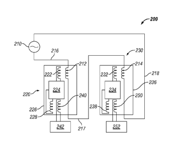
[0025] Figure 2 shows a schematic view of a system 200 of that includes a
power source 210 and two electrical systems 220, 230 that receive inductive
power in
accordance with certain example embodiments. In one or more embodiments, one
or
more of the components shown in Figure 2 may be omitted, repeated, and/or
6
CA 02903049 2015-08-27
WO 2014/137816
PCT/US2014/019472
substituted. Accordingly, embodiments of inductive power transmission should
not
be considered limited to the specific arrangements of components shown in
Figure 2.
For example, a third enclosure could be electrically connected in series with
the first
enclosure 220 and the second enclosure 230.
[0026] The system 200 of Figure 2 includes a power source 210
(substantially
similar to the power source 110 described above with respect to Figure 1) and
two
inductors (i.e., inductor 212 and inductor 214, also substantially similar to
the
inductors described above with respect to Figure 1) that are electrically
connected in
series (in a "daisy chain" formation) using conductors 216, 217, 218. As shown
in
Figure 2, inductor 212 is located inside of enclosure 226, and inductor 214 is
located
inside of enclosure 236. These components (the power source 210, the inductor
212,
and the inductor 214) can be equated to the primary portion 101 described
above with
respect to Figure 1. In certain example embodiments, the power source 210 can
be
any source of power causing current to flow through the inductor 212 and the
inductor
214. Examples of such a source of power can include, but is not limited to, a
cable
(as shown in Figures 4A and 4B), an electrical connector (as shown in Figure
5), a
battery, and a 120 VAC wall outlet.
[0027] Electrical system 220 includes an inductor 222 that is positioned
within
an enclosure 226 and that is electromagnetically coupled to inductor 212. The
electrical system 220 also includes circuitry 224 (also positioned within the
enclosure
226) that is electrically connected to inductor 222 and inductor 228, inductor
240
(also positioned within the enclosure) that is electromagnetically coupled to
inductor
228, and circuitry 242 (also positioned outside the enclosure) that is
electrically
connected to inductor 240. Similarly, electrical system 230 includes an
inductor 232
that is positioned within an enclosure 236 and that is electromagnetically
coupled to
inductor 214. The electrical system 230 also includes circuitry 234 (also
positioned
within the enclosure) that is electrically connected to inductor 232 and
inductor 238,
inductor 250 (also positioned within the enclosure) that is
electromagnetically coupled
to inductor 238, and circuitry 252 (also positioned outside the enclosure)
that is
electrically connected to inductor 250. Each of electrical system 220 and
electrical
system 230 can be equated to the secondary portion 102 described above with
respect
to Figure 1.
[0028] Referring to electrical system 220, while one end of the inductor
222 is
electrically connected to circuitry 224, the other end of inductor 222 can be
7
CA 02903049 2015-08-27
WO 2014/137816
PCT/US2014/019472
electrically connected to a different portion of the device 224, or
electrically
connected to some other component or device. The device 224 can include one or
more of a number of electrical devices that use current and/or voltage to
operate.
Examples of such devices can include, but are not limited to, a VFD, a
breaker, a
motor starter, a switch, an air moving device, a controller, a sensor, a
motor, and a
protective device. Similarly, with respect to electrical system 230, while one
end of
the inductor 232 is electrically connected to device 234, the other end of
inductor 232
can be electrically connected to a different portion of the device 234, or
electrically
connected to some other component or device. The device 234 can include one or
more of a number of electrical devices that use current and/or voltage to
operate.
[0029] Similar to the process described above with respect to Figure 1,
the
power source 210 generates current that flows through conductor 216 to
inductor 212.
When this occurs, inductor 222, which is located proximately to inductor 212,
is
electromagnetically induced to generate an amount of power based on the
current
flowing through inductor 212. The power induced in the inductor 222 is used to
power up some or all of the device 224 within the enclosure 226.
[0030] After current flows through inductor 212, the current continues to
flow
through conductor 217 to inductor 214. When the current flows through inductor
214,
electrical system 230 can receive power induced by inductor 214. Specifically,
as
current flows through inductor 214, inductor 232, which is located proximately
to
inductor 214, is electromagnetically induced to generate an amount of power
based on
the current flowing through inductor 214. The power induced in the inductor
232 is
used to power up some or all of the device 234 within the enclosure 236.
[0031] After current flows through inductor 214, the current continues to
flow
through conductor 218 to return to the power source 210, completing the
electric
circuit. Optionally, other inductors can be placed in series with, and/or in
parallel
with, inductors 212 and 214. Similarly, other electrical systems, similar to
electrical
systems 220 and 230, can be included in the system 200 and receive power
induced
by such additional inductors.
[0032] Optionally, one or both electrical systems 220 and 230 can be a
source
of inductive power for one or more additional devices. For example, as shown
in
Figure 2, electrical system 220 includes an inductor 228 that receives power
from
device 224, which in this case acts as a power source for inductor 228. In
such a case,
inductor 240, which is located proximately to inductor 228, is
electromagnetically
8
CA 02903049 2015-08-27
WO 2014/137816
PCT/US2014/019472
induced to generate an amount of power based on the current flowing through
inductor 228. The power induced in the inductor 240 is used to power up some
or all
of the device 242, which is electrically connected to inductor 240.
[0033] While one end of the inductor 228 is electrically connected to
device
224, the other end of inductor 228 can be electrically connected to a
different portion
of the device 224, or electrically connected to some other component or
device.
Further, while one end of the inductor 240 is electrically connected to device
242, the
other end of inductor 240 can be electrically connected to a different portion
of the
device 242, or electrically connected to some other component or device. The
device
242 can include one or more of a number of electrical devices that use current
and/or
voltage to operate.
[0034] Similarly, as shown in Figure 2, electrical system 230 includes an
inductor 238 that receives power from device 234, which in this case acts as a
power
source for inductor 238. In such a case, inductor 250, which is located
proximately to
inductor 238, is electromagnetically induced to generate an amount of power
based on
the current flowing through inductor 238. The power induced in the inductor
250 is
used to power up some or all of the device 252, which is electrically
connected to
inductor 250.
[0035] While one end of the inductor 238 is electrically connected to
device
234, the other end of inductor 238 can be electrically connected to a
different portion
of the device 234, or electrically connected to some other component or
device.
Further, while one end of the inductor 250 is electrically connected to device
252, the
other end of inductor 250 can be electrically connected to a different portion
of the
device 252, or electrically connected to some other component or device. The
device
252 can include one or more of a number of electrical devices that use current
and/or
voltage to operate.
[0036] Figure 3 shows a schematic view of a system 300 of lighting devices
receiving inductive power in accordance with certain example embodiments.
Specifically, the system 300 of Figure 3 includes a power source 310, lighting
device
A 320, lighting device B 330, lighting device C 340, and lighting device D 350
formed in a "daisy chain" formation. In one or more embodiments, one or more
of
the components shown in Figure 3 may be omitted, repeated, and/or substituted.
Accordingly, embodiments of inductive power transmission should not be
considered
9
CA 02903049 2015-08-27
WO 2014/137816
PCT/US2014/019472
limited to the specific arrangements of components shown in Figure 3. For
example,
fewer or additional lighting sources can be included in the system 300.
[0037] The power source 310 is substantially similar to the power source
110
described above with respect to Figure 1. In addition, inductor 312, which is
electrically connected to the power source 310, is positioned inside of
lighting device
A 320 and is substantially similar to the inductors described above with
respect to
Figures 1 and 2. Not shown (hidden from view) are three other inductors, one
positioned inside of each of lighting device B 330, lighting device C 340, and
lighting
device D 350. The power source 310, inductor 312, and the three hidden
conductors
are electrically connected in series using conductors 370, 371, 372, 373, and
374.
These components (the power source 310, inductor 312, and the three hidden
inductors) can be equated to the primary portion 101 described above with
respect to
Figure 1. Inductor 312 and the three hidden conductors can be called a
transmitting
inductor or a primary inductor.
[0038] Lighting device A 320 includes an inductor 322 (also called a
receiving inductor or a secondary inductor) that is positioned within an
enclosure 326
and that is electromagnetically coupled to inductor 312. Lighting device A 320
also
includes device 324 (also positioned within the enclosure 326) that is
electrically
connected to inductor 322. Similarly, lighting device B 330, lighting device C
340,
and lighting device D 350 each includes an inductor (hidden from view inside
the
enclosure), positioned within the respective enclosure (enclosure 336,
enclosure 346,
enclosure 356) that is electromagnetically coupled to an inductor electrically
connected to the power source 310 and inductor 312, and electrically connected
to
device (also hidden from view inside the enclosure). Each of lighting device A
320,
lighting device B 330, lighting device C 340, and lighting device D 350 can be
equated to the secondary portion 102 described above with respect to Figure 1.
[0039] Referring to lighting device A 320, while one end of the inductor
322
is electrically connected to circuitry 324, the other end of inductor 322 can
be
electrically connected to a different portion of the circuitry 324, or
electrically
connected to some other component or device. The circuitry 324 can include one
or
more of a number of electrical devices that use current and/or voltage to
operate.
Examples of such devices can include, but are not limited to, a LED driver, a
controller, and a photocell sensor. The inductor and/or circuitry of lighting
device B
CA 02903049 2015-08-27
WO 2014/137816
PCT/US2014/019472
330, lighting device C 340, and lighting device D 350 can be substantially
similar to
the corresponding components of lighting device A 320.
[0040] Similar to the process described above with respect to Figure 1,
the
power source 310 generates current that flows through conductor 370 to
inductor 312.
When this occurs, inductor 322, which is located proximately to inductor 312,
is
electromagnetically induced to generate an amount of power based on the
current
flowing through inductor 312. The power induced in the inductor 322 is used to
power up some or all of the circuitry 324 within the enclosure 326.
[0041] After current flows through inductor 312, the current continues to
flow
through conductor 371 to the transmitting inductor positioned within lighting
device
B 330. When the current flows through the transmitting inductor positioned
within
lighting device B 330, the circuitry positioned within the enclosure 336 of
lighting
device B 330 can receive power induced by the transmitting inductor through
the
electromechanically-coupled receiving inductor that is electrically connected
to the
circuitry of lighting device B 330. Similarly, conductor 372 is used to
transmit the
current flowing through the transmitting inductor positioned in lighting
device B 330
to the transmitting inductor positioned in lighting device C 340. When the
current
flows through the transmitting inductor positioned within lighting device C
340, the
circuitry positioned within the enclosure 346 of lighting device C 340 can
receive
power induced by the transmitting inductor through the electromechanically-
coupled
receiving inductor that is electrically connected to the circuitry of lighting
device C
340.
[0042] Subsequently, conductor 373 is used to transmit the current flowing
through the transmitting inductor positioned in lighting device C 340 to the
transmitting inductor positioned in lighting device D 350. When the current
flows
through the transmitting inductor positioned within lighting device D 350, the
circuitry positioned within the enclosure 356 of lighting device D 350 can
receive
power induced by the transmitting inductor through the electromechanically-
coupled
receiving inductor that is electrically connected to the circuitry of lighting
device D
350. Finally, conductor 374 is used to transmit the current flowing through
the
transmitting inductor positioned in lighting device D 350 back to the power
source
310.
[0043] In certain example embodiments, input voltage for certain secondary
circuits is designed to compensate for voltage drop. Voltage drop can be
caused by
11
CA 02903049 2015-08-27
WO 2014/137816
PCT/US2014/019472
one or more of a number of factors, including but not limited to length of one
or more
conductors, size of one or more conductors, ambient temperature, number of
secondary circuits, power usage of a secondary circuit, and material of a
conductor.
For example, in the lighting system of Figure 3, the current flowing through
the
transmitting inductor of lighting device D 350 is less than the current
flowing through
the transmitting inductor of lighting device A 320. Thus, compensation may
need to
be made so that the circuitry of lighting device D 350 operates properly for
the
voltage induced in the receiving inductor of lighting device D 350.
[0044] Figures 4A and 4B show various views of a system 400 using an
inductive device in accordance with certain example embodiments. Specifically,
Figure 4A shows a side view in partial cross-section of the system 400 as the
inductive device is approaching a closed position. In addition, Figure 4B
shows a
cross-sectional front view of the system 400 as the inductive device is
approaching
the closed position. In one or more embodiments, one or more of the components
shown in Figures 4A and 4B may be omitted, repeated, and/or substituted.
Accordingly, embodiments of inductive power transmission should not be
considered
limited to the specific arrangements of components shown in Figures 4A and 4B.
For
example, another device (e.g., a motor winding, a battery) can be used in
place of the
cable in the system 400.
[0045] Referring to Figures 4A and 4B, the system 400 includes the
inductive
device and a cable 430. The cable 430 can be any device through which current
flows. In this example, the cable 430 includes a conductor 434 that is
disposed within
(surrounded by) insulating member 432. The conductor 434 can be made of one or
more of a number of electrically conductive materials, including but not
limited to
copper and aluminum. The conductor 434 can be one or more of a number of sizes
(e.g., 10 American wire gauge (AWG), 12 AWG, 16 AWG). The conductor 434 can
be a single conductor or one of a number of conductors (strands) within the
insulating
member 432.
[0046] The insulating member 432 of the cable 430 can be made of one or
more of a number of electrically non-conductive materials, including but not
limited
to rubber and plastic. In certain example embodiments, the insulating member
432 is
made of such material as to allow the encroacher 416 (described below) to
penetrate
(e.g., strip, pierce) at least a portion of the insulating member 432 in order
to make
physical contact with the conductor 434. The insulating member 432 that
surrounds
12
CA 02903049 2015-08-27
WO 2014/137816
PCT/US2014/019472
the conductor 434 can be of any thickness. Further, the thickness of the
insulating
member 432 can be substantially uniform along the length and/or perimeter of
the
insulating member 432.
[0047] The inductive device can include a housing 410 and a latch assembly
420. The housing 410 can include at least one wall 412 that forms a cavity.
Inside of
the cavity of the housing 410 can be disposed a receiving inductor 414. The
receiving
inductor 414 can be electrically connected to any circuitry and/or device
positioned
inside of and/or outside of the housing 410, where such circuitry and/or
device can be
substantially similar to those described above with respect to Figures 2 and
3. The
wall 412 can be made of one or more of a number of suitable materials,
including but
not limited to plastic, steel, aluminum, and rubber.
[0048] In certain example embodiments, the housing 410 of the inductive
device also includes a encroacher 416 disposed on the outer surface of the
wall 412.
The encroacher 416 can be any device or component that can physically contact
the
conductor 434 through the insulating member 432. The encroacher 416 can
contact
the conductor 434 in one or more of a number of ways. For example, the
encroacher
416 can strip away the insulating member 432. As another example, the
encroacher
416 can stab through the insulating member 432.
[0049] The encroacher 416 can be positioned in such a location on the
outer
surface of the wall 412 that allows the encroacher 416 to contact the
insulating
member 432 of the cable 430. In this example, the encroacher 416 is disposed
on the
bottom side of the housing 410. The encroacher 416 can have at least one
sharpened
edge 417 that is shaped and sized in such a way as to penetrate the insulating
member
432 of the cable 430. The encroacher 416 may penetrate part of the thickness
of the
insulating member 432 or all of the thickness of the insulating member 432. In
the
latter case, the encroacher 416 can contact the conductor 434 of the cable
430.
[0050] In order for the encroacher 416 to penetrate the insulating member
432,
the encroacher 416 can be made of one or more of a number of suitable
materials,
including but not limited to stainless steel and aluminum. In certain example
embodiments, the encroacher 416 can be made of an electrically conductive
material.
The encroacher 416 can form a single piece with the wall 412 (as from a mold),
or the
encroacher 416 can be a separate piece coupled to the wall 412. In the latter
case, the
encroacher 416 can be mechanically coupled to the wall 412 in one or more of a
number of ways, including but not limited to fixedly, slidably, removably, and
13
CA 02903049 2015-08-27
WO 2014/137816
PCT/US2014/019472
detachably. The encroacher 416 can be mechanically coupled to the wall 412
using
one or more of a number of coupling methods, including but not limited to
welding,
epoxy, fastening devices (e.g., screws, nuts), and mating threads.
[0051] In certain example embodiments, the housing 410 of the inductive
device also includes a coupling feature 418 disposed on the outer surface of
the wall
412. The coupling feature 418 can be one or more of a number of features that
can be
used to couple part of the latch assembly 420 to the housing 410, as described
below.
The coupling feature 418 can be any of a number of features, including but not
limited
to a protrusion, an aperture, a slot, a mating thread, and a slotted cap. In
this example,
the coupling feature 418 is a protrusion that extends away from the back side
of the
wall 412 toward the bottom of the housing 410.
[0052] The coupling feature 418 can be made of one or more of a number of
suitable materials, including but not limited to plastic, stainless steel, and
aluminum.
The coupling feature 418 can form a single piece with the wall 412 (as from a
mold),
or the coupling feature 418 can be a separate piece coupled to the wall 412.
In the
latter case, the coupling feature 418 can be mechanically coupled to the wall
412 in
one or more of a number of ways, including but not limited to fixedly,
slidably,
removably, and detachably. The coupling feature 418 can be mechanically
coupled to
the wall 412 using one or more of a number of coupling methods, including but
not
limited to welding, epoxy, fastening devices (e.g., screws, nuts), and mating
threads.
[0053] In certain example embodiments, the latch assembly 420 of the
inductive device includes an arm 424, a harness 426, and a latch 428. The
latch
assembly 420 can be movably coupled to the housing 410 using the arm 424. The
arm 424 can have a length and can have one or more of a number of segments.
For
example, as shown in Figures 4A and 4B, the arm 424 has two segments, one
positioned on each side of the harness 426 and the housing 410. The arm 424 of
the
latch assembly 420 can be movably (e.g., hingedly, slidably) coupled to the
housing
410 in one or more of a number of ways. In this example, a pin 422 protrudes
through
an aperture in the proximal end of the arm 424 (or in each segment of the arm
424) as
well as an aperture through part or all of the wall 412 in the housing 410. In
such a
case, the arm 424 becomes hingedly coupled to the housing 410 and rotates
about the
pin 422. In addition, or in the alternative, one or more other features can be
disposed
on the wall 412 and/or the arm 424 to allow the housing 410 to become moveably
coupled to the latch assembly 420.
14
CA 02903049 2015-08-27
WO 2014/137816
PCT/US2014/019472
[0054] In certain example embodiments, the harness 426 couples to the
insulating member 432 of the cable 410. Specifically, the harness 426 provides
leverage so that the encroacher 418, positioned on substantially the opposite
side of
the cable 430, can more easily penetrate the insulating member 432 of the
cable 430.
Further, the harness 426 can be used to secure the inductive device to the
cable 430
when the latch 428 is mechanically coupled to the coupling feature 418.
[0055] The harness 426 can have dimensions (e.g., thickness, width,
length,
curvature) suitable for securing the cable 430. If the arm 424 has multiple
segments,
then the harness 426 can be mechanically coupled to all or some of such
segments.
For example, as shown in Figures 4A and 4B, the harness 426 is mechanically
coupled at one end one segment of the arm 424 and at the other end to the
other
segment of the arm 424. The harness 426 can be mechanically coupled to the arm
424 at any point (or, if there are multiple harnesses 426, at any points)
along the arm
424. For example, as shown in Figure 4A, the harness 426 is coupled to the arm
424
toward the distal end of the arm 424. In addition, the harness 426 can extend
away
from the arm 424 in one or more directions. In this case, as shown in Figure
4A, the
harness 426 extends radially outward from the arm 424.
[0056] In certain example embodiments, the harness 426 and/or the arm 424
include one or more features that help secure the latch assembly 420 to the
cable 430.
For example, the segments of the arm 424 can have angled spikes along the
interior-
facing outer surface of the arm 424, where the angled spikes can penetrate at
least a
portion of the thickness of the insulating member 432.
[0057] In certain example embodiments, the latch 428 mechanically couples
to the coupling feature 418 of the housing 410. The latch 428 can be of any
shape
and/or size suitable to mechanically couple to the coupling feature 418. In
this
example, as shown in Figure 4A, the latch 428 includes a notch 429 that
protrudes in
such a manner as to allow the notch 429 on the latch 428 to fit over the top
of the
coupling feature 418 (in this case, a protrusion) and secure the latch
assembly 420 to
the housing 410. The latch 428 can be one or more features disposed on the arm
424.
The latch 428 can be located at any of a number of points along the length of
the arm
424. In this example, the latch 428 is a protruding element that extends
radially
inward (i.e., toward the bottom side of the cable 430 when the cable 430 is
positioned
between the arm 424, the harness 426, and the housing 410) from the arm 424 at
the
distal end of the arm 424.
CA 02903049 2015-08-27
WO 2014/137816
PCT/US2014/019472
[0058] The components (e.g., arm 424, harness 426, latch 428) of the latch
assembly 420 can be made from one or more of a number of materials, including
but
not limited to plastic, metal, and rubber. The latch assembly 420 can be made
from a
single piece (as from a mold) or can be made of multiple pieces that are
mechanically
coupled to each other in one or more of a number of ways, including but not
limited to
fixedly, slidably, removably, and detachably. In such a case, the multiple
pieces of
the latch assembly 420 can be mechanically coupled to each other using one or
more
of a number of coupling methods, including but not limited to welding, epoxy,
fastening devices (e.g., screws, nuts), and mating threads.
[0059] Figure 5 shows an electrical connector 500 using inductive power
transmission in accordance with certain example embodiments. In one or more
embodiments, one or more of the components shown in Figure 5 may be omitted,
repeated, and/or substituted. Accordingly, embodiments of an electrical
connector
using inductive power transmission should not be considered limited to the
specific
arrangements of components shown in Figure 5.
[0060] Referring to Figures 4 and 5, the electrical connector 500 includes
a
first connector end 510 (e.g., a male connector end) and a second connector
end 530
(e.g., a female connector end). The first connector end 510 includes a sleeve
528 that
has an open end and forms a cavity. The sleeve 528 acts as a type of housing
for the
other components of the first connector end 510, described below. The sleeve
528
can be rigid and/or flexible. The sleeve 528 can be made of one or more of a
number
of materials, including but not limited to rubber, plastic, and metal.
[0061] Inside of the cavity can be disposed an insulator 520. In certain
example embodiments, the insulator 520 physically separates each of the
conductors
(described below) and the associated inductive devices from the other
conductors and
associated inductive devices that are positioned within the cavity. The
insulator 520
can be rigid or slightly flexible. In the latter case, the channels formed
within the
insulator 520 and through which the conductors and associated inductive
devices arc
disposed substantially maintain their integrity with respect to each other so
that the
channels do not make contact with each other. The insulator 520 can be made of
one
more of a number of materials, including but not limited to rubber, nylon,
plastic,
foam, and silicon. In certain example embodiments, the insulator 520 is made
of
electrically non-conductive material.
16
CA 02903049 2015-08-27
WO 2014/137816
PCT/US2014/019472
[0062] The insulator 520 can fill any portion or all of the cavity formed
by the
sleeve 528. For example, as shown in Figure 5, the insulator 520 can make
contact
with a back portion of the sleeve 528, but not contact the sides of the sleeve
528. In
addition, the insulator 520 can be recessed within the sleeve 528 (as shown in
Figure
5), can extend to substantially the end of the sleeve 528 (where the open end
is
located), or can extend beyond the end of the sleeve 528 (as shown with the
insulator
540 of the second connector end 530 in Figure 5).
[0063] One or more conductors can be positioned within one or more
channels
of the insulator 520. For example, as shown in Figure 5, there are three
conductors
(i.e., conductor 514, conductor 516, and conductor 518) positioned within the
insulator 520 of the first connector end 510. The conductors can be part of a
cable
511 that is mechanically coupled to the sleeve 528. The cable 511 can include
an
insulating member 512. The conductor and insulating member 512 of the cable
can
be substantially similar to the conductor 434 and insulating member 432 of the
cable
430 described above with respect to Figures 4A and 4B.
[0064] In certain example embodiments, the distal end of each conductor is
electrically connected to an inductive device. For example, in this case, the
distal
ends of conductor 514, conductor 516, and conductor 518 are electrically
connected to
a separate inductive device. Each inductive device can include a housing and a
transmitting inductor. For example, as shown in Figure 5 the inductive device
electrically connected to conductor 514 includes a housing 522 that houses a
transmitting inductor 523. The inductive device electrically connected to
conductor
516 includes a housing 524 that houses a transmitting inductor 525. The
inductive
device electrically connected to conductor 518 includes a housing 526 that
houses a
transmitting inductor 527. Each inductive device can be substantially similar
to, or
different from, the other inductive devices in the first connector end 510.
[0065] As a result of a conductor being electrically connected to an
inductive
device, when current flows through the inductor (e.g., inductor 514), then
current also
flows through the associated transmitting inductor (e.g., transmitting
inductor 523) of
the inductive device. In certain example embodiments, one or more of the
inductive
devices are surrounded by the insulator 520. In other words, the insulator may
prevent the inductive devices from being physically exposed to ambient air.
Further,
the insulator 520 maintains a physical separation from each of the inductive
devices
of the first connector end 510.
17
CA 02903049 2015-08-27
WO 2014/137816
PCT/US2014/019472
[0066] The components of the second connector end 530 are substantially
the
same as the corresponding components of the first connector end 510. The
second
connector end 530 of Figure 5 includes a sleeve 548 that forms a cavity.
Disposed
within this cavity are three conductors (conductor 534, conductor 536, and
conductor
538) and associated inductive devices that are physically separated from each
other by
an insulator 540. In this case, the inductive devices of the second connector
end 530
include a receiving inductor within the housing. Specifically, the inductive
device
electrically connected to the distal end of conductor 534 includes receiving
inductor
543 positioned within housing 542. The inductive device electrically connected
to the
distal end of conductor 536 includes receiving inductor 545 positioned within
housing
544. The inductive device electrically connected to the distal end of
conductor 538
includes receiving inductor 547 positioned within housing 546.
[0067] As mentioned previously, the insulator 520 of the first connector
end
510 is recessed within the sleeve 528, and the insulator 540 of the first
connector end
530 extends beyond the end of the sleeve 548. The inductive devices of the
first
connector end 510 and the second connector end 530 are positioned proximate to
the
open end of the sleeve 528 and the open end of the sleeve 548, respectively.
When
the first connector end 510 is mechanically coupled to the second connector
end 530,
the inductive devices of the first connector end 510 are positioned
proximately to the
corresponding inductive devices of the second connector end 530.
[0068] For example, as shown in Figure 5, the transmitting inductor 522 of
the
first connector end 510 is positioned proximately to (abuts against) the
receiving
inductor 542 of the second connector end 530. When this occurs, and when
current
flows through the conductor 514, current is induced in the receiving inductor
542
because the receiving inductor 542, located proximately to the transmitting
inductor
522, is electromagnetically coupled to the transmitting inductor 522. Thus,
the
current induced in the receiving inductor 542 flows through conductor 534 and
on to
whatever device and/or circuit the cable 532 is electrically connected.
[0069] As with any example embodiments of inductive power transmission
described herein, the distance between a transmitting inductor (e.g.,
transmitting
inductor 522) and a receiving inductor (e.g., receiving inductor 542) can vary
based
on one or more of a number of factors. Such factors can include, but are not
limited
to, the material (e.g., copper, aluminum) of each inductor, the power
requirements of
18
CA 02903049 2015-08-27
WO 2014/137816
PCT/US2014/019472
the load fed by the receiving inductor, the temperature and humidity of the
environment in which the inductors are located, and the size of each inductor.
[00701 In certain example embodiments, the sleeve 528 and/or the sleeve
548
include one or more coupling features. Specifically the sleeve 528 can include
a
coupling feature, and the sleeve 548 can include a coupling feature that
complements
the coupling feature of the sleeve 528. In such a case, the coupling features
can fasten
(mechanically couple) the sleeve 528 of the first connector end 510 to the
sleeve 548
of the second connector end 530. Examples of such coupling features can
include, but
are not limited to, clips, protrusions, fastening devices, apertures, slots,
and mating
threads. The coupling features can be positioned at any location on the
connector
ends, such as the outer surface, along the open end, and along an inner
surface.
[0071] Example electrical connectors using inductive power, such as the
electrical connector 500, have several advantages. For one, the amount of
force used
to mechanically couple the first connector end 510 to the second connector end
530
can be extremely low. In other words, because the electrical connector 500
does not
require the mating of conductor pins and pin receivers, as is found in
electrical
connectors known in the art. The only mechanical mating of the connector ends
in the
electrical connector 500 is inserting the protruding insulator 540 of the
second
connector end 540 into the space left between the retracted insulator 520 and
the
sleeve 528 of the first connector end 510.
[0072] Another advantage is that coupling and decoupling (insertion and
removal) of the first connector end 510 and the second connector end 530
results in
little to no mechanical wear of the connector ends and their components (e.g.,
insulator 520, receiving inductor 544). Because there is little or no
mechanical wear
of the connector ends of the example electrical connector 500, the electrical
connector
500 can function for longer periods of time without the need to replace,
maintain,
and/or repair the electrical connector 500.
[0073] In addition, or in the alternative, the use of example inductive
power
transmission systems, methods, and/or devices described herein provide other
advantages. For example, example inductive power transmission systems,
methods,
and/or devices can be used in a "daisy chain" formation to have a single
source of
power (e.g., a battery, a conductor) provide power, through an electromagnetic
coupling with example inductive devices, to other circuits and/or devices. By
using
inductive power transmission, power can be provided to one or more of a number
of
19
CA 02903049 2015-08-27
WO 2014/137816
PCT/US2014/019472
circuits and/or devices (including other transmitting inductors) using an
existing
infrastructure and without the need for additional sources of power. Thus, a
single
conductor and/or a single piece of equipment can be used to provide power to
one or
more of a number of circuits and/or devices without terminating at each
circuit and/or
device.
[0074] Example embodiments also reduce or eliminate temperature rise in
electrical connectors and/or connections that result from hard terminations of
conductors to provide power to various circuits and/or devices. In other
words, by
using inductive power transmission, terminations of conductors can be reduced
or
eliminated, which reduces the likelihood of failure of an electrical
connection caused
by one or more of a number of factors, including but not limited to corrosion,
overheating, mechanical wear, mechanical strain, and vibration. Thus, because
temperature rise in electrical connectors and/or connections is reduced or
eliminated,
costs related to labor, materials, time, lost opportunity, and/or other
similar
considerations can be reduced or eliminated.
[0075] Example embodiments also improve safety for electrical systems. For
example, terminations that fail can cause a fault and/or other adverse
electrical
operating condition. Such conditions can lead to dangerous conditions such as
an
explosion. In such a case, by using example embodiments, explosions and other
adverse operating conditions can be reduced or avoided. Thus, injuries to
users can
be reduced and/or eliminated. In addition, the operating integrity of
equipment in an
electrical system using example embodiments can be increased.
[0076] Accordingly, many modifications and other embodiments set forth
herein will come to mind to one skilled in the art to which inductive power
transmission for electrical devices pertain having the benefit of the
teachings
presented in the foregoing descriptions and the associated drawings.
Therefore, it is
to be understood that inductive power transmission for electrical devices are
not to be
limited to the specific embodiments disclosed and that modifications and other
embodiments are intended to be included within the scope of this application.
Although specific terms are employed herein, they are used in a generic and
descriptive sense only and not for purposes of limitation.