Note: Descriptions are shown in the official language in which they were submitted.
ANTIREFLECTIVE COATING FOR GLASS APPLICATIONS AND
METHOD OF FORMING SAME
CROSS-REFERENCE TO RELATED PATENT APPLICATION
Some references, which may include patents, patent applications and various
publications, are cited and discussed in the description of this invention.
The citation and/or
discussion of such references is provided merely to clarify the description of
the disclosure and
is not an admission that any such reference is "prior art" to the disclosure
described herein. In
tenns of notation, hereinafter, "Inl" represents the nth reference cited in
the reference list. For
example, [5] represents the 5th reference cited in the reference list, namely,
C. S. Thompson, R.
A. Fleming, M. Zou, Transparent self-cleaning and antifogging silica
nanoparticle films, Solar
Energy Materials and Solar Cells 115 (2013) 108-113.
FIELD OF THE DISCLOSURE
The disclosure relates generally to applications of polymers, and more
particularly
1
Date Recue/Date Received 2020-08-04
CA 02903248 2015-08-31
WO 2014/134594 PCT/US2014/019806
to nanostructured antireflective coating, methods of forming the
nanostructured
antireflective coating, and applications of the nanostructured antireflective
coating in
glass devices including solar panels and photovoltaic devices.
BACKGROUND OF THE DISCLOSURE
The background description provided herein is for the purpose of generally
presenting the context of the disclosure. Work of the presently named
inventors, to the
extent it is described in this background section, as well as aspects of the
description that
may not otherwise qualify as prior art at the time of filing, are neither
expressly nor
.. impliedly admitted as prior art against the disclosure.
The air-glass interface at the surface of a packaged solar panel can reflect a
significant amount of the incident light, resulting in a significant drop in
the power output
of the panel. One method of reducing this loss is to utilize antireflective
coatings. Single
layer antireflective coatings (ARC) have been reported using porous silica
films with an
index of refraction of approximately n = 1.23 [I]. However, the reflectance
from these
coatings can only be minimized at a single wavelength. In order to reduce
these losses,
the optical reflectance must be minimized over a large range of wavelengths.
Recent developments in graded index, or "moth-eye" coatings promise wide-band
antireflection characteristics. In these coatings, the percent area of solid
material varies
continuously from 0% at the interface with the incident medium to 100% at some
depth
in the coating due to surface topography [6-8]. The effective index of
refraction at any
depth in the coating can be calculated using an effective medium
approximation. This
behavior mimics the wide-band antireflective behavior of moths eyes which are
covered
with cylindrical structures arranged in a hexagonal array with a diameter of
around 240
nm [6]. Li et al. produced these structures on glass substrates using reactive
ion etching
with polystyrene beads as an etching mask and achieved transmittance of 98%
from 300-
800 nm [7]. Du et al. utilized a chemical treatment to induce graded index
behavior at
the surface of glass substrates resulting in transmittance of greater than
98%. However,
the chemical process requires 13 hours of submersion in a caustic solution
[8].
2
CA 02903248 2015-08-31
WO 2014/134594 PCT/US2014/019806
Silica nanoparticle films are widely used as antireflective coatings on solar
cell
cover glass [1-3] due to the porosity induced low index of refraction.
However, the
capability to deposit these films from aqueous solutions is one of challenges
preventing
application in industrial processes [4].
Therefore, a heretofore unaddressed need exists in the art to address the
aforementioned deficiencies and inadequacies.
SUMMARY OF THE DISCLOSURE
Certain aspects of the disclosure are directed to nanostructured
antireflective
coating, methods for forming the nanostructured antireflective coating, and
applications
of the nanostructured antireflective coating in solar panels and photovoltaic
devices.
In one aspect of the disclosure, a method for forming an antireflective
coating on
a substrate includes the steps of (a) providing a polyvinylpyrrolidone (PVP)
solution and
a silica solution; (b) depositing the PVP solution on a surface of the
substrate to forming
a PVP film thereon; and (c) depositing the silica solution on the formed PVP
film on the
substrate to form a silica film thereon, thereby forming a stack structure
having the silica
film formed on the PVP film that is, in turn, formed on the substrate.
In one embodiment, the PVP film dissolves in the silica solution of the silica
film
as the silica film is formed on the PVP film.
In one embodiment, the method further includes, prior to depositing the PVP
solution, cleaning the substrate. In one embodiment, the cleaning step is
performed by
ultra-sonication.
In one embodiment, each of the depositing steps (a) and (b) is performed by a
dip
coating process.
In one embodiment, the method further includes drying the stack structure to
form
the antireflective coating on the substrate, where the antireflective coating
comprises
silica nanoparticles uniformly adhered on the surface of the substrate. In one
embodiment, the drying step is performed at a temperature in a range of about
10-
1200 C.
3
CA 02903248 2015-08-31
WO 2014/134594 PCT/US2014/019806
In one embodiment, the substrate is formed of glass.
In one embodiment, the PVP solution has a concentration of the PVP in a range
of
about 1-20 wt%.
In one embodiment, the PVP film has a thickness in a range of about 5-300 nm.
In one embodiment, the silica film has a thickness in a range of about 5-300
nm.
In another aspect of the disclosure, a method for forming an antireflective
coating
on a substrate includes the steps of (a) providing a polymer solution and a
silica solution
having silica nanoparticles; (b) depositing the polymer solution on a surface
of the
substrate to forming a polymer film thereon; and (c) depositing the silica
solution on the
formed polymer film on the substrate to form a silica film thereon, thereby
forming a
stack structure having the silica film formed on the polymer film that is, in
turn, formed
on the substrate
In one embodiment, the substrate is formed of a transparently dielectric
material
having a refractive index, ns. In one embodiment, the polymer solution
contains a
transparent polymer having a refractive index, np, wherein the refractive
index np of the
transparent polymer is between the refractive index of air and the refractive
index n, of
the dielectric material..
In one embodiment, the substrate is formed of glass. In one embodiment, the
transparent polymer comprises polyvinylpyrrolidone (PVP), polyethylene,
poly(methyl
methacrylate) (PMMA), polystyrene, polypropylene, polysiloxanes,
polyvinylalcohol,
polyamide, Ethylene vinyl acetate (EVA), or a combination of them.
In one embodiment, the transparent polymer is soluble. In one embodiment, the
polymer film dissolves in the silica solution of the silica film as the silica
film is formed
on the polymer film. In one embodiment, the silica nanoparticles are uniformly
adhered
on the surface of the substrate.
In one embodiment, the transparent polymer is insoluble. In one embodiment,
the
silica nanoparticles are uniformly adhered on the polymer film that is formed
on the
surface of the substrate.
In one embodiment, the polymer solution has a concentration of the transparent
4
CA 02903248 2015-08-31
WO 2014/134594 PCT/US2014/019806
polymer in a range of about 1-20 wt%.
In one embodiment, the polymer film has a thickness in a range of about 5-300
nm. In one embodiment, the silica film has a thickness in a range of about 5-
300 nm.
In one embodiment, the method further includes, prior to depositing the PVP
solution, cleaning the substrate. In one embodiment, the cleaning step is
performed by
ultra-sonication.
In one embodiment, each of the depositing steps (a) and (b) is performed by a
dip
coating process.
In one embodiment, the method further includes drying the stack structure. In
one
embodiment, the drying step is performed at a temperature in a range of about
10-
1200 C.
In yet another aspect of the disclosure, an antireflective coating is formed
on a
substrate according to the above disclosed method.
In a further aspect of the disclosure, a solar panel includes at least one
antireflective coating, as disclosed above.
In yet a further aspect of the disclosure, a photovoltaic device includes at
least one
antireflective coating, as disclosed above.
These and other aspects of the disclosure will become apparent from the
following description of the preferred embodiment taken in conjunction with
the
following drawings, although variations and modifications therein may be
affected
without departing from the spirit and scope of the novel concepts of the
disclosure.
BRIEF DESCRIPTION OF THE DRAWINGS
The accompanying drawings illustrate one or more embodiments of the disclosure
and together with the written description, serve to explain the principles of
the disclosure.
Wherever possible, the same reference numbers are used throughout the drawings
to refer
to the same or like elements of an embodiment.
FIG. 1A shows a flowchart for forming an antireflective coating according to
one
embodiment of the disclosure.
5
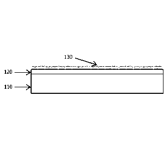
FIG. 1B shows schematically a cross-section view of an antireflective coating
according to one embodiment of the disclosure.
FIG. IC shows schematically a cross-section view of an antireflective coating
according to another embodiment of the disclosure.
FIG. 2 shows schematically a thin film stack utilized to model reflectance and
transmittance of PVP adhesion layer and silica nanoparticle coating according
to one
embodiment of the disclosure. This coating is applied on both sides of the
glass substrate
during dip coating.
FIG. 3 shows modeled transmittances with various thicknesses of silica
nanoparticle antireflective coating and 200 nm thick PVP adhesion layer
according to one
embodiment of the disclosure. The AM 1.5 solar spectrum is shown for
reference.
FIG. 4 shows optimized transmittances of silica nanoparticle coating with and
without PVP adhesion layer according to one embodiment of the disclosure. The
modeled
transmittances are shown for reference.
FIG. 5A shows current-voltage curves for crystalline silicon solar cells
without a
cover glass, packaged with a bare glass, and packaged with a glass coated with
200 nm PVP
and 130 nm SiO2 layers according to one embodiment of the disclosure.
FIG. 5B shows current-voltage curves for crystalline silicon solar cells
packaged
with a bare glass, and packaged with a glass coated with PVP and SiO2 layers
according to
one embodiment of the disclosure.
FIG. 6 shows AFM scans of (a) silica nanoparticle films and (b) PVP enhanced
silica nanoparticle films on glass substrates according to one embodiment of
the
disclosure.
FIG. 7 shows cross sections of AFM scans for a silica film (a) and a PVP
enhanced silica film (b) according to one embodiment of the disclosure.
FIG. 8 shows bearing area curves for a silica nanoparticle film and a PVP
enhanced silica nanoparticle film according to one embodiment of the
disclosure.
FIG. 9 shows optical transmittance spectra for a silica nanoparticle film and
a
PVP enhanced silica nanoparticle film according to one embodiment of the
disclosure.
FIG. 10 shows reflectance spectra for a silica nanoparticle film and a PVP
enhanced silica nanoparticle film according to one embodiment of the
disclosure.
6
Date Recue/Date Received 2020-08-04
CA 02903248 2015-08-31
WO 2014/134594 PCT/US2014/019806
DETAILED DESCRIPTION OF THE DISCLOSURE
The disclosure will now be described more fully hereinafter with reference to
the
accompanying drawings, in which exemplary embodiments of the disclosure are
shown.
This invention may, however, be embodied in many different forms and should
not be
construed as limited to the embodiments set forth herein. Rather, these
embodiments are
provided so that this disclosure will be thorough and complete, and will fully
convey the
scope of the disclosure to those skilled in the art. Like reference numerals
refer to like
elements throughout.
The terms used in this specification generally have their ordinary meanings in
the
art, within the context of the disclosure, and in the specific context where
each term is
used. Certain terms that are used to describe the disclosure are discussed
below, or
elsewhere in the specification, to provide additional guidance to the
practitioner regarding
the description of the disclosure. For convenience, certain terms may be
highlighted, for
example using italics and/or quotation marks. The use of highlighting and/or
capital
letters has no influence on the scope and meaning of a term; the scope and
meaning of a
term are the same, in the same context, whether or not it is highlighted
and/or in capital
letters. It will be appreciated that the same thing can be said in more than
one way.
Consequently, alternative language and synonyms may be used for any one or
more of
the terms discussed herein, nor is any special significance to be placed upon
whether or
not a term is elaborated or discussed herein. Synonyms for certain terms are
provided. A
recital of one or more synonyms does not exclude the use of other synonyms.
The use of
examples anywhere in this specification, including examples of any terms
discussed
herein, is illustrative only and in no way limits the scope and meaning of the
disclosure or
of any exemplified term. Likewise, the disclosure is not limited to various
embodiments
given in this specification.
It will be understood that when an element is referred to as being "on"
another
element, it can be directly on the other element or intervening elements may
be present
therebetween. In contrast, when an element is referred to as being "directly
on" another
element, there are no intervening elements present. As used herein, the term
"and/or"
7
CA 02903248 2015-08-31
WO 2014/134594 PCT/US2014/019806
includes any and all combinations of one or more of the associated listed
items.
It will be understood that, although the terms first, second, third, etc. may
be used
herein to describe various elements, components, regions, layers and/or
sections, these
elements, components, regions, layers and/or sections should not be limited by
these
terms. These terms are only used to distinguish one element, component,
region, layer or
section from another element, component, region, layer or section. Thus, a
first element,
component, region, layer or section discussed below can be termed a second
element,
component, region, layer or section without departing from the teachings of
the
disclosure.
It will be understood that when an element is referred to as being "on",
"attached"
to, "connected" to, "coupled" with, "contacting", etc., another element, it
can be directly
on, attached to, connected to, coupled with or contacting the other element or
intervening
elements may also be present. In contrast, when an element is referred to as
being, for
example, "directly on", "directly attached" to, "directly connected" to,
"directly coupled"
with or "directly contacting" another element, there are no intervening
elements present.
It will also be appreciated by those of skill in the art that references to a
structure or
feature that is disposed "adjacent" to another feature may have portions that
overlap or
underlie the adjacent feature.
The terminology used herein is for the purpose of describing particular
embodiments only and is not intended to be limiting of the disclosure. As used
herein,
the singular forms "a", "an" and "the" are intended to include the plural
forms as well,
unless the context clearly indicates otherwise. It will be further understood
that the terms
"comprises" and/or "comprising", or "includes" and/or "including" or "has"
and/or
"having" when used in this specification specify the presence of stated
features, regions,
integers, steps, operations, elements, and/or components, but do not preclude
the presence
or addition of one or more other features, regions, integers, steps,
operations, elements,
components, and/or groups thereof.
Furthermore, relative terms, such as "lower" or "bottom" and "upper" or "top",
may be used herein to describe one element's relationship to another element
as
8
CA 02903248 2015-08-31
WO 2014/134594 PCT/US2014/019806
illustrated in the figures. It will be understood that relative terms are
intended to
encompass different orientations of the device in addition to the orientation
shown in the
figures. For example, if the device in one of the figures is turned over,
elements
described as being on the "lower" side of other elements would then be
oriented on the
"upper" sides of the other elements. The exemplary term "lower" can,
therefore,
encompass both an orientation of lower and upper, depending on the particular
orientation of the figure. Similarly, if the device in one of the figures is
turned over,
elements described as "below" or "beneath" other elements would then be
oriented
"above" the other elements. The exemplary terms "below" or "beneath" can,
therefore,
encompass both an orientation of above and below.
Unless otherwise defined, all terms (including technical and scientific terms)
used
herein have the same meaning as commonly understood by one of ordinary skill
in the art
to which this invention belongs. It will be further understood that terms,
such as those
defined in commonly used dictionaries, should be interpreted as having a
meaning that is
consistent with their meaning in the context of the relevant art and the
disclosure, and
will not be interpreted in an idealized or overly formal sense unless
expressly so defined
herein.
As used herein, "around", "about", "substantially" or "approximately" shall
generally mean within 20 percent, preferably within 10 percent, and more
preferably
within 5 percent of a given value or range. Numerical quantities given herein
are
approximate, meaning that the terms "around", "about", "substantially" or
"approximately" can be inferred if not expressly stated.
As used herein, the terms "comprise" or "comprising", "include" or
"including",
"carry" or "carrying", "has/have" or "having", "contain" or "containing",
"involve" or
"involving" and the like are to be understood to be open-ended, i.e., to mean
including
but not limited to.
As used herein, the phrase "at least one of A, B, and C" should be construed
to
mean a logical (A or B or C), using a non-exclusive logical OR. It should be
understood
that one or more steps within a method may be executed in different order (or
9
CA 02903248 2015-08-31
WO 2014/134594 PCT/US2014/019806
concurrently) without altering the principles of the disclosure.
As used herein, the term, "nano-sized material", refers to an object of
intermediate size between molecular and microscopic (micrometer-sized)
materials. In
describing nano-sized materials, the sizes of the nano-sized materials refer
to the number
of dimensions on the nanoscale. For example, nanotextured surfaces have one
dimension
on the nanoscale, i.e., only the thickness of the surface of an object is
between 1.0 and
1000.0 nm. Nanowires have two dimensions on the nanoscale, i.e., the diameter
of the
tube is between 1.0 and 1000.0 nm; its length could be much greater. Finally,
sphere-like
nanoparticles have three dimensions on the nanoscale, i.e., the particle is
between 1.0 and
1000.0 nm in each spatial dimension. A list of nano-sized materials includes,
but are not
limited to, nanoparticle, nanocomposite, quantum dot, nanofilm, nanoshell,
nanofiber,
nanowire, nanotree, nanobush, nanotube, nanoring, nanorod, and so on.
The description below is merely illustrative in nature and is in no way
intended to
limit the disclosure, its application, or uses. The broad teachings of the
disclosure can be
implemented in a variety of forms. Therefore, while this disclosure includes
particular
examples, the true scope of the disclosure should not be so limited since
other
modifications will become apparent upon a study of the drawings, the
specification, and
the following claims. For purposes of clarity, the same reference numbers will
be used in
the drawings to identify similar elements. It should be understood that one or
more steps
within a method may be executed in different order (or concurrently) without
altering the
principles of the disclosure.
OVERVIEW
The cover glass used in solar cell packaging can reflect a significant amount
of
light, resulting in lower device efficiencies and decreased power output. In
order to
reduce the loss of the power output of the packaged solar cells (panel) due to
reflectance
at an air-glass interface of the panel, antireflective coatings are applied on
the packaging
(cover) glass.
Using the Fresnel equations, the ideal antireflective coating for a glass-air
CA 02903248 2015-08-31
WO 2014/134594 PCT/US2014/019806
interface should have an index of refraction of n = 1.23 [1]. The lowest index
of
refraction solid thin film coating available is MgF2 with n = 1.38. A lower
index film is
achievable using nanoparticle coatings due to the presence of porosity that
lowers the
bulk index of refraction [2]. This relationship is shown below:
n = ¨ d2 ¨ 1) + 1 ,
where np and nd are the indices of refraction for the porous and dense films,
respectively,
and p is the porosity fraction.
Silica nanoparticle films are widely used as antireflective coatings on a
solar cell
cover glass [1-3] due to the porosity induced low index of refraction.
However, the
capability to deposit these films from aqueous solutions is one of challenges
preventing
application in industrial processes [4].
According to the disclosure, the use of a transparent polymer as an adhesion
layer
can facilitate the deposition of a uniform silica nanoparticle antireflective
film on a
substrate. The transparent polymer acts as a surface modification to the
substrate
allowing increased wettability of the surface with aqueous coating solutions.
In certain embodiments, suitable polymers are selected based on the index of
refraction being sufficiently close to the dielectric substrate to be coated
and having
sufficiently high optical transmittance. In certain embodiments, the substrate
is formed
of a transparently dielectric material having a refractive index, us. In
certain
embodiments, the suitable polymers are those having a refractive index, np,
which is
between the refractive index of air and the refractive index ns of the
dielectric material.
In certain embodiments, the refractive index np of the transparent polymer is
equal or
substantially approximate to the refractive index n, of the dielectric
material. In certain
embodiments, these polymers would be compatible with solution processing
methods.
However, other methods can also be utilized to practice the invention.
In certain embodiments, the dielectric substrate is a glass substrate
(n5=1.5).
Accordingly, the transparent polymers, such as polyvinylpyrrolidone (PVP),
polyethylene, poly(methyl methacrylate) (PMMA), polystyrene, polypropylene,
polysiloxanes, polyvinylalcohol, polyamide, ethylene vinyl acetate (EVA), or a
11
CA 02903248 2015-08-31
WO 2014/134594 PCT/US2014/019806
combination of them, whose refractive indices, as listed in Table I, are equal
or
substantially approximate to the refractive index ns =1.5 of the glass
substrate, can be
utilized as the adhesion layer.
Table I: Polymers and its Index of Refraction
Polymer Refractive Index np
Polyethylene ¨1.5
PMMA ¨1.49
Polystyrene ¨1.5
Polypropylene ¨1.49
Polysiloxanes 1.4-1.54
Polyvinylalcohol ¨1.5
Polyamide ¨1.5
EVA ¨1.47
FIG. lA illustrates the process/method of forming an antireflective coating on
a
substrate, with the use of a transparent polymer as the adhesion layer,
according to one
embodiment of the disclosure. The process/method includes the following steps:
at step
S110, a polymer solution and a silica solution are provided. The polymer
solution has a
concentration of the transparent polymer in a range of about 1-20 wt%. The
silica
solution contains a colloidal silica solution.
At step S120, the polymer solution is deposited on a surface of the substrate
to
forming a polymer film thereon. In certain embodiments, the polymer film has a
thickness in a range of about 5-300 nm.
At step S130, the silica solution is deposited on the formed polymer film on
the
substrate to form a silica film thereon, thereby forming a stack structure
having the silica
film formed on the polymer film that is, in turn, formed on the substrate. In
certain
embodiments, the silica film has a thickness in a range of about 5-300 nm.
In certain embodiments, each of the depositing steps S120 and S130 is
performed
12
CA 02903248 2015-08-31
WO 2014/134594 PCT/US2014/019806
by a dip coating, spray coating, or roll coating process, or any combination
thereof.
In certain embodiments, prior to depositing the polymer solution, the
substrate
may need to be cleaned, which can be performed by ultra-sonication, or self-
cleaning.
At step S140, the stack structure is dried to form the antireflective coating
on the
substrate, wherein the antireflective coating comprises silica nanoparticles.
In certain
embodiments, the drying step S140 is performed at a temperature in a range of
about 10-
1200 . For example, the drying step S140 can be performed by placing the stack
structure in room temperature, or by heating the stack structure to the
temperature in the
range of about 10-1200 . In certain embodiments, the heating process can
enhance the
durability/strength of the film due to calcification.
In certain embodiments, the transparent polymer is insoluble. Accordingly, the
silica nanoparticles 130 of the antireflective coating are uniformly adhered
on the
polymer film 120 that is formed on the surface of the substrate 110, as shown
in FIG. 1B.
In certain embodiments, the transparent polymer, e.g., PVP, is soluble. During
the process, the polymer film may dissolve in the silica solution of the
silica film as the
silica film is formed on the polymer film. Accordingly, the silica
nanoparticles 130 of
the antireflective coating are uniformly adhered on the surface of the
substrate 110, as
shown in FIG. 1C.
The above disclosed process can be applied to solar cells (panels) and
photovoltaic devices to form one or more nanostructured antireflective coating
on the
packaging substrates so as to reduce the loss of the power output of the
packaged solar
cells (panels) and the photovoltaic devices due to the reflectance at the air-
substrate
interfaces of the solar cells (panels) and the photovoltaic devices.
In certain embodiments, the polymer PVP is used as an adhesion layer for
silica
nanoparticle antireflective glass coatings. The PVP has an index of refraction
close to
soda lime glass and exhibits excellent film forming qualities, and is found to
significantly
increase the uniformity of the deposited silica nanoparticle film and results
in an average
transmittance of greater than about 98% in the wavelength range of about 450-
1100 nm.
Silica nanoparticle coatings deposited without the PVP layer resulted in an
average
13
CA 02903248 2015-08-31
WO 2014/134594 PCT/US2014/019806
transmittance of only about 95%. When the PVP/SiO2 coated glass is used to
package a
crystalline silicon solar cell, the short circuit current is increased to
about 36.97 inA/cm2
from about 35.42 mA/cm2 for the same cell packaged with a bare glass.
Among other things, the invention can find applications in a variety of
fields, such
as building glass, biological applications, solar devices, and the like.
Without intent to limit the scope of the disclosure, exemplary examples and
their
related results according to the embodiments of the disclosure are given
below. Note that
titles or subtitles may be used in the examples for convenience of a reader,
which in no
way should limit the scope of the disclosure. Moreover, certain theories are
proposed and
disclosed herein; however, in no way they, whether they are right or wrong,
should limit
the scope of the disclosure so long as the disclosure is practiced according
to the
disclosure without regard for any particular theory or scheme of action.
EXAMPLE 1
SILICA NANOPARTICLE ANTIREFLECTIVE COATING WITH PVP
ADHESION LAYER
According to the disclosure, in order to reduce the loss of the power output
of a
packaged solar panel due to reflectance at an air-glass interface of the
panel,
antireflective coatings are applied on the packaging (cover) glass.
In this exemplary example, a transparent polymer, such as PVP, is used as an
adhesion layer for silica nanoparticle antireflective glass coatings. The
adhesion layer of
PVP is deposited prior to dip coating in an aqueous silica nanoparticle
solution. Thin
films of PVP have an index of refraction (n = 1.48) that is very similar to
glass (n = 1.5)
which reduces reflection at the glass-PVP interface. PVP is a water soluble
polymer that
has been used in literature to improve the wettability of aqueous coating
solutions. PVP
also bonds easily to both the glass substrate and the nanoparticle film. These
characteristics improve both the uniformity and antireflective performance of
silica
nanoparticle coatings while maintaining compatibility with scalable deposition
technologies based on solution processing. In this example, PVP was found to
14
CA 02903248 2015-08-31
WO 2014/134594 PCT/US2014/019806
significantly increase the uniformity of the deposited silica nanoparticle
film and results
in an average transmittance of greater than 98% in the wavelength range of 450-
1100 nm.
Silica nanoparticle coatings deposited without the PVP layer resulted in an
average
transmittance of 95%. Further, when the PVP/5i02 coated glass was used to
package a
crystalline silicon solar cell, the short circuit current was increased to
36.97 mA/cm2 from
35.42 mA/cm2 for the same cell packaged with bare glass.
SAMPLE FABRICATION
In this example, PVP (40,000 MW, AMRESCO, USA) is used as an adhesion
layer to facilitate the deposition of a uniform silica nanoparticle
antireflective film on
soda-lime glass microscope slides (No. 8201, Ted Pella, USA) following the
procedure
outlined in FIG. 1A. The optical properties of these substrates are then
characterized, and
the best performers are used to package a commercially available crystalline
silicon solar
cell for electrical characterization.
The glass substrates were cleaned by sonication in methanol for about 10
minutes
to remove any surface contamination, and then dried by blowing with nitrogen.
Samples
to be coated with the polymer adhesion layer were then dip coated in a
solution of about
1 wt% PVP in methanol at withdrawal rate of about 50 mm/min. This results in a
PVP
film thickness of about 200 nm. All samples were then dipped in a colloidal
silica
solution (SNOWTEX, Nissan Chemical, USA) that had been diluted to about 5 wt%.
The withdrawal rate was varied from about 10 to 80 mm/min to deposit different
thicknesses of 5i02 nanoparticle layer on the surface. All samples were dried
in an oven
at about 120 C for about 5 minutes to remove any remaining moisture from the
film.
RESULTS AND DISCUSSION
Modeling: A commercial spectroscopy software package (FilMeasure, Filmetrics,
Inc., USA) was utilized to model the transmittance spectrum of the samples as
a function
of the SiO2 nanoparticle coating thickness. The samples were modeled as a
double sided
coating with PVP thickness of about 200 nm and SiO2 thicknesses from about 100-
180
CA 02903248 2015-08-31
WO 2014/134594 PCT/US2014/019806
nm. An exemplary thin film stack is shown in FIG. 2, where each side of the 1
mm thick
glass substrate (n=1.5) is coated with a PVP layer (n=1.48) with a thickness
of 200 nm,
which in turn, is coated with a SiO2 layer (1.23) with a thickness of 120 nm.
Previous
work by the inventors had developed optical properties databases for both the
silica
nanoparticle films and PVP thin films [51.
The modeled transmittances (320, 330, 340, 350 and 360) with various
thicknesses (100 nm, 120 nm, 140 nm, 160nm and 180nm) of the silica
nanoparticle
antireflective coating and a 200 nm thick PVP adhesion layer are shown in FIG.
3, where
the AM 1.5 solar spectrum (390) is shown for reference. It can be determined
from these
data that the thickness of the SiO2 nanoparticle coating has significant
influence over the
location of the maximum transmittance peak. All nanoparticle coating
thicknesses
improved the average transmittance from 450-1050 nm by more than 8%. When
compared with the AM 1.5 solar spectrum, it is apparent that the SiO2 coating
with a
thickness of about 120 nm provides the greatest increase in the transmitted
solar energy.
Optical Characterization: The transmittance of the coated samples was measured
using a spectrophotometer (aRTie, Filmetrics, USA) with a measurement range of
about
350-1050 nm. The average transmittance of various samples is shown in Table
II. The
use of PVP/SiO2 coating increases the transmittance of glass by about 9.56%,
far greater
than the 5.45% increase seen with SiO2 alone.
Table II: Transmittance (Tavg) improvement
Tavg
SiO2 thickness Improvement
PVP 450-1050 nm
(nm) (%)
(%)
no 0 90.04 N/A
no 150 94.94 5.44
no 190 94.95 5.45
yes 120 98.27 9.14
yes 130 98.65 9.56
16
CA 02903248 2015-08-31
WO 2014/134594 PCT/US2014/019806
The transmittance spectra of the samples with the highest transmittance both
with
and without the PVP adhesion layer are shown in FIG. 4. The model
transmittance (410)
for a 120 nm thick SiO2 coating with a 200 nm thick PVP adhesion layer is
shown to
have very good agreement with the measured results (420) in wavelength range
of 550-
850 nm.
The film thicknesses were calculated using the reflectance spectra. The PVP
thickness was confirmed to be about 200 nm, with the SiO2 coating thickness
varying
between about 120 and about 190 nm depending on the dipping conditions. These
values
are shown in Table 1. The use of PVP as an adhesion layer resulted in thinner
silica
nanoparticle films that were significantly more uniform. The greatest
transmittance
improvement is realized for films with PVP adhesion layer and 130 nm silica
nanoparti cl e films.
Electrical Characterization: A test rig was designed that allows a small (2.5
cm2)
crystalline silicon solar cell (Model No. 276-124, RadioShack, USA) to be
packaged with
interchangeable glass covers. The sample was illuminated with a small-area
class-B solar
simulator (PV Measurements, Inc., USA) at AM 1.5 (100 mW/cm2). The current-
voltage
characteristics were measured using a Keithley 2400 source meter.
By packaging the solar cell with plain glass, both the short circuit current
and
efficiency of the packaged cell are reduced by more than 10%. When the cover
glass is
replaced with glass coated with 200 nm thick PVP and 130 nm thick 5i02 layers,
over
60% of those losses are recovered. The current voltage curves for a solar cell
packaged
with no cover (curve 510), bare glass (curve 520), and PVP/SiO2 coated glass
(curve 530)
are shown in FIG. 5.
The open circuit voltage, short circuit current density, and efficiency
measurements are shown in Table III. The use of glass coated with 200 nm thick
PVP
and 130 nm thick SiO2 layers results in an increase in the short circuit
current to 14.87
mA/cm2 from 13.90 mA/cm2 for bare glass. The overall efficiency of the
selected solar
cell is also increased to 5.47% from 5.13%.
17
CA 02903248 2015-08-31
WO 2014/134594 PCT/US2014/019806
Table III: Current-voltage characteristics
Sample Voc (V) Jse (mA/cm2) Efficeiency (%)
Cell only 0.574 15.48 5.71
Bare Glass 0.571 13.90 5.13
PVP/SiO2 0.573 14.87 5.47
SUMMARY
According to this exemplary example, the use of a transparent polymer adhesion
layer significantly increases the effectiveness of a silica nanoparticle
antireflective
coating. The used polymer PVP has an index of refraction close to soda lime
glass and
exhibits excellent film forming qualities. By depositing a 200 nm thick PVP
adhesion
layer on the soda lime glass (substrate) prior to depositing a 130 nm thick
silica
nanoparticle coating, the transmittance of the regular soda lime glass is
increased from
about 90.04% to about 98.65%. The improved transmittance demonstrates that the
coating is highly antireflective through the use of an aqueous silica
nanoparticle solution.
The improved optical properties lead to a higher short circuit current and
efficiency of a
crystalline silicon solar cell than when packaged with regular glass. In
certain
embodiments, over about 60% of the losses associated with packaging the cell
with glass
are recovered when packaged with PVP/SiO2 coated glass.
EXAMPLE 2:
NANOSTRUCTURED PVP/5IO2 ANTIREFLECTIVE COATING FOR SOLAR
PANEL APPLICATIONS
Porous silica nanoparticle ARCs deposited by dip coating in aqueous solutions
have been reported previously [5] and is a promising alternative to more
expensive
deposition processes. The water soluble polymer, PVP, has been used in
literature to
improve the wettability and uniformity of aqueous silica coating solutions
[4]. PVP is
transparent, and has an index of refraction of n=1.48, which is very close to
that of the
18
CA 02903248 2015-08-31
WO 2014/134594 PCT/US2014/019806
glass substrate (n=1.5). This limits reflection at the glass-PVP interface.
In this example, the water soluble polymer PVP is used as an adhesion layer in
the
deposition of silica nanoparticle films from aqueous solutions. A
nanostructured
antireflective coating is created using a simple aqueous dip coating method.
The addition
of PVP as an adhesion layer is shown to significantly impact the formation of
nanostructures on the surface of the coating. Bearing analysis using atomic
force
microscopy (AFM) is utilized as a method of characterizing the surface
topography that
results in a graded index behavior. The resulting variation in surface
roughness creates a
layer with a graded index of refraction. These films create an antireflective
surface that
increases the optical transmittance of glass substrates from about 94.5% for
silica
nanoparticle films to about 98.6% for PVP enhanced silica nanoparticle films
at about
500 nm wavelength.
SAMPLE FABRICATION
Silica nanoparticle films were fabricated on soda-lime glass substrates (No.
8201,
Ted Pella, USA). The glass substrates were cleaned by ultra-sonication in
methanol for
about 10 minutes to remove surface contamination and then dried by blowing
with
nitrogen.
Samples to be coated with silica nanoparticle films are then dipped in a
colloidal
silica solution (SNOWTEX, Nissan Chemical, USA) that has been diluted to about
5
wt% by addition of deionized water. The withdrawal rates for these samples
were
optimized at about 80 mm/min in previous studies [5].
PVP enhanced films were deposited by first dip coating substrates at a rate of
about 50 mm/min in a 5 wt% PVP (40,000 MW, AMRESCO, USA) in methanol
solutions. The PVP coated substrates were then immediately dipped in about 5
wt%
colloidal silica solution with a withdrawal rate of about 10 min/min. This
withdrawal
rate has been chosen to maintain a constant total film thickness between the
PVP
enhanced silica films and the silica films without PVP.
All samples were dried at about 140 C in an oven to remove residual water
from
19
CA 02903248 2015-08-31
WO 2014/134594 PCT/US2014/019806
the coating.
RESULTS AND DISCUSSION
Atomic Force Microscopy (AFM): AFM was used to characterize the surface
topography of the coatings. The scans were taken in a tapping mode with a
silicon probe
(RTESPA, Bruker, USA) at a scan rate of about 1 Hz. The AFM characterization
of the
samples with and without PVP as an adhesion layer shows distinct differences
in the
topography of the surfaces, as shown in FIG. 6.
For silica nanoparticle films without PVP, the surface includes individual 50
nm
particles visible in the AFM scan, as shown in FIG. 6(a). When PVP is used as
an
adhesion layer, the particles form agglomerates that are approximately 200 nm
in
diameter, as shown in FIG. 6(b). In addition, silica films without PVP are
relatively
smooth with large micron-sized pores, as shown in FIG. 6(a). With the addition
of PVP,
the surface roughness becomes more regular with a reduction in the occurrence
of large
.. pores, as shown in FIG. 6(b).
Cross sections of these scans are shown in FIG. 7. It can be seen that the
surface
roughness of silica films without PVP is dominated by the particle size of
approximately
50 nm with peak-to-valley distance close to 50 nm. However, for samples that
have PVP
adhesion layers, the peak-to-valley distance is close to 100 nm. The Ra and R4
values
.. calculated for the entire AFM images are shown in Table IV.
Table IV: Roughness Parameters From AFM Scans
Roughness Parameter SiO2 Only PVP+Si02
Ra 9.l nm 15.6 nm
Rq 11.7 nm 20.3 nm
Bearing Analysis: Bearing analysis is an effective method to characterize
.. nanoporosity of a sample surface. In the bearing analysis, the AFM image is
analyzed to
determine the percentage of area that is filled with material as a function of
height. The
CA 02903248 2015-08-31
WO 2014/134594 PCT/US2014/019806
outputs of the bearing analysis for samples with a PVP adhesion layer (curve
820) and
without a PVP adhesion layer (curve 810) are shown in FIG. 8. The increased
roughness
and porosity of the surface of the PVP enhanced silica nanoparticle films
results in a lower
slope of the bearing curve (820) and a larger distance over which the bearing
area changes.
This effective distance for silica nanoparticle films is approximately 50 nm.
For the PVP
enhanced silica nanoparticle films, the effective distance is approximately
100 nm.
Based on the bearing analysis, the PVP enhanced silica films demonstrate
better
antireflective behavior than the silica films without PVP since the effective
distance over
which a continuously changing refractive index can be expected is
approximately
doubled.
Optical Characterization: The optical transmittance and reflectance of the
samples was characterized using a simultaneous reflectance and transmittance
spectrophotometer (aRTie, Filmetrics, USA). The transmittance was measured
over a
wavelength range of about 350-1050 nm.
Optical transmittance spectra for silica nanoparticle and PVP enhanced silica
nanoparticle films are shown in FIG. 9. The average transmittance over the
range of
interest for silicon based photovoltaic devices (550-1050 nm) is about 88.5%
for bare
glass (curve 910). The addition of a silica nanoparticle film increases the
transmittance to
about 95.0% (curve 920). The PVP enhanced silica films result in an additional
increase
.. in transmittance to about 97.2% (curve 930).
The significance of this increase is more apparent when the transmittance at a
wavelength of about 500 nm, the peak wavelength of the solar spectrum, is
considered.
The PVP enhanced silica films increase the optical transmittance to about
98.6% at the
wavelength of about 500 nm. The transmittance of the bare glass and silica
coated glass at
the wavelength of about 500 nm are about 90.7% and 94.5%, respectively.
The average reflectance from 550-1050 nm for the bare glass is about 7.1%
(curve
1010). The silica nanoparticle films reduce the reflectance in this range to
about 4.96%
(curve 1020). The addition of PVP as an adhesion layer further reduces the
reflectance to
an average of about 1.07% (curve 1030) from 550-1050 nm. The reflectance for
the bare
21
CA 02903248 2015-08-31
WO 2014/134594
PCT/US2014/019806
glass, the glass coated with silica nanoparticle film and the glass coated
with PVP
enhanced silica nanoparticle films, at 500 nm wavelength is about 7.85%,
5.44%, 0.83%,
respectively. Due to the increased distance over which a graded index of
refraction is
present in the PVP enhanced silica films, the antireflective behavior is
minimized over a
larger range of wavelengths, as shown in FIG. 10.
SUMMARY
According to this exemplary example, the use of PVP as an adhesion layer
during
deposition of silica nanoparticle antireflective coatings directly impacts the
surface
topography and increases the optical transmittance. The PVP adhesion layer
results in
the agglomeration of nanoparticles and results in a higher surface roughness
that
increases the graded index antireflective effect. The graded index behavior of
the silica
nanoparticle coatings was related to the atomic force microscope topography
measurements using bearing analysis. The PVP enhanced silica nanoparticle
films on a
soda-lime glass are found to transmit about 98.6% of incident light at the 500
nm
wavelength, compared to only about 90.7% for the bare glass and about 94.5%
for the
silica nanoparticle coated glass. The increase in transmittance is the result
of reflectance
being reduced to about 0.83% for the PVP enhanced silica films at the 500 nm
wavelength due to the increase in surface roughness.
The foregoing description of the exemplary embodiments of the disclosure has
been presented only for the purposes of illustration and description and is
not intended to
be exhaustive or to limit the disclosure to the precise forms disclosed. Many
modifications and variations are possible in light of the above teaching.
The embodiments were chosen and described in order to explain the principles
of
the disclosure and their practical application so as to enable others skilled
in the art to
utilize the disclosure and various embodiments and with various modifications
as are
suited to the particular use contemplated. Alternative embodiments will become
apparent
to those skilled in the art to which the disclosure pertains without departing
from its spirit
and scope. Accordingly, the scope of the disclosure is defined by the appended
claims
22
CA 02903248 2015-08-31
WO 2014/134594 PCT/US2014/019806
rather than the foregoing description and the exemplary embodiments described
therein.
REFERENCE LIST
[1] F. C. Cebeci, Z. Wu, L. Zhai, R. E. Cohen, M. F. Rubner, Nanoporosity-
driven
superhydrophilicity: A means to create multifunctional antifogging coatings,
Langmuir 22 (2006) 2856-2862.
[2] W. Shimizu, Y. Murakami, Microporous silica thin films with low
refractive
indices and high young's modulus, ACS Appl. Mater. Interfaces 2 (2010) 3128-
3133.
[3] X. Lu, Z. Wang, Z. Yang, X. Xu, L. Zhan, N. Zhao, et al., Antifogging
and
antireflective silica film and its application on solar modules, Surf. Coat.
Technol.
206 (2011) 1490-1494.
[4] H. Kozuka, A. Yamano, M. Fujita, H. Uchiyama, Aqueous dip-coating route
to
dense and porous silica thin films using silica nanocolloids with an aid of
polyvinylpyrrolidone, J. Sol-Gel Sci. Technol. 61(2012) 381-389.
[5] C. S. Thompson, R. A. Fleming, M. Zou, Transparent self-cleaning and
antifogging silica nanoparticle films, Solar Energy Materials and Solar Cells
115
(2013) 108-113.
[6] A. R. Parker, H. E. Townley, Biomimetics Of Photonic Nanostructures,
Nature
Nanotechnology 2, (2007) 347-353.
[7] Y. Li, J. Zhang, S. Zhu, H. Dong, F. Jia, Z. Wang, Z. Sun, L. Zhang, Y.
Li, H. Li,
W. Xu, B. Yang, Biomimetic Surfaces For High-Performance Optics, Advanced
Materials 21 (2009) 4731-4734.
[8] Y. Du, H. He, Y. Jin, F. Kong, H. Guan, Z. Fan, Graded porous glasses
for
antireflective applications formed by chemical treatment, Applied Surface
Science 258 (2012) 6431-6435.
23