Note: Descriptions are shown in the official language in which they were submitted.
CA 02903981 2017-02-17
SYSTEM AND METHOD FOR MULTIPLEXED AND
BUFFERED MINIATURIZED SENSOR ARRAYS
[0001] [Continue to next paragraph]
FIELD OF THE INVENTION
[0002] The present invention relates to multiplexed miniaturized sensor
arrays, in
particular buffered miniaturized sensor arrays.
BACKGROUND OF THE INVENTION
[0003] Pressure sensing equipment is often used within the aerodynamic
research field. The sensing equipment may be used in many applications such as
windtunnel, flight test, and turbomachinery testing. For example, sensing
equipment
may be used in wind tunnel applications during the development of wing
designs.
Pressure sensing equipment may also be used for in-flight test applications
such as
monitoring the pressure conditions observed by a test missile, both around the
missile
and in crucial engine areas such as the inlet, combustor, and nozzle. For
aerodynamic
research, miniature pressure measurement instrumentation may be used that
incorporates piezoresistive pressure sensor arrays of individual sensors.
These
miniature instruments, also called pressure scanners, may incorporate
1
CA 02903981 2015-09-03
WO 2014/138030 PCT/US2014/020231
electronic multiplexers at the product's sensor substrate level for individual
sensor
selection to connect to an attached amplifier or other electronic circuit.
Current state
of the art miniature pressure scanners include the ESP line of miniature
pressure
scanners (e.g ESP-16HD, ESP-32HD, and ESP-64HD miniature pressure scanners)
manufactured by Measurement Specialties, Inc. Pressure Systems and as
described
in the ESP Pressure Scanner User's Manual, dated August 2009, the subject
matter
thereof incorporated herein by reference in its entirety.
[0004] In a typical application, hundreds or even thousands of individual
pressure sensors may be used and monitored in an aerospace application, with
Bipolar and CMOS based multiplexers typically considered for such scanning
needs.
The need to scan across these sensors through the multiplexer at increasingly
faster
speeds has highlighted several problems relating to fast sensor settling times
for
pressure scanners. Limiting factors include a multiplexer's inherent charge
injection,
capacitance and resistance characteristics, and the pressure sensors'
relatively high
source impedance. In particular, during switching, voltage spikes are created
on the
multiplexed signals coming from each pressure sensor and through the
multiplexer.
These spikes must settle and decay in order for the signal line to return to
its true
value so that an accurate reading may be made. In addition, it has been
observed
that when pressure sensing equipment is used at higher ambient temperatures,
the
settling time for the voltage spikes is increased.
2
CA 02903981 2015-09-03
WO 2014/138030 PCT/US2014/020231
[0005] Alternate systems and methods for miniature electronic pressure
scanning that reduce the settling time of multiplexer voltage spikes are
desired.
SUMMARY OF THE INVENTION
[0006] A miniature pressure scanning system may comprise: a plurality of
miniature pressure sensors including a plurality of sensor outputs, each of
the
miniature pressure sensors including at least one pressure sensor output for
providing an analog output signal and each at least one sensor output having
an
associated output impedance; a plurality of buffers, each buffer electrically
coupled
to one sensor output of the plurality of sensor outputs and providing a
buffered
sensor output, and each buffer configured to reduce the associated output
impedance of the one sensor output coupled to it; and at least one multiplexer
downstream of each said buffer and configured to multiplex the buffered analog
output pressure to provide a multiplexed analog signal for output to another
device.
[0007] The plurality of buffers may comprise a plurality of transistors
and
plurality of bias resistors, and each buffer coupled to one sensor output may
comprise one of the plurality of transistors and one of the plurality of bias
resistors.
In an embodiment, one or both of the one of the plurality of transistors and
the one
of the plurality of bias resistors may be integral to the one of the plurality
of miniature
pressure sensors it is buffering. In another embodiment, one or both of the
one of
the plurality of transistors and the one of the plurality of bias resistors
may be
3
CA 02903981 2015-09-03
WO 2014/138030 PCT/US2014/020231
configured as a bare die element mounted on a substrate of the miniature
pressure
scanning system. Each of the plurality of transistors may be a one of a
bipolar
junction transistor, a field-effect transistor, a metal oxide semiconductor
field-effect
transistor, and an insulated-gate bipolar transistor. In one embodiment, the
at least
one multiplexer may have at least 16 input channels. The at least one
multiplexer
may also be operative to be switched at a rate of 50 micro seconds per
buffered or
unbuffered sensor output or faster. Each buffer may be configured to reduce
the
associated output impedance of the sensor output coupled to it by at least two
orders of magnitude.
[0008] A method for sensing pressure may comprise: sensing pressure using
a plurality of miniature pressure sensors including a plurality of sensor
outputs, each
of the plurality of miniature pressure sensors having at least one sensor
output for
providing an analog output signal and each at least one sensor output having
an
associated output impedance; buffering the at least one sensor output of at
least
some of the plurality of miniature pressure sensors and providing a buffered
sensor
output, thereby reducing the associated output impedance of each buffered
sensor
output; multiplexing, using at least one multiplexer, the plurality of
buffered sensor
outputs; and switching between channels of the at least one multiplexer,
thereby
reading the analog output signal of each buffered sensor output of the
plurality of
sensor outputs.
4
CA 02903981 2015-09-03
WO 2014/138030 PCT/US2014/020231
[0009] Buffering the at least one sensor output of at least some of the
plurality
of miniature pressure sensors may comprise electrically coupling one of a
plurality of
transistors and one of a plurality of bias resistors to each sensor output
being
buffered. In an embodiment, one or both of the one of the plurality of
transistors and
the one of the plurality of bias resistors may be integral to a substrate of
the one of
the plurality of miniature pressure sensors whose sensor output is being
buffered. In
another embodiment, one or both of the one of the plurality of transistors and
the
one of the plurality of bias resistors may be configured as a bare die element
mounted on a substrate of the miniature pressure scanning system. Each of the
plurality of transistors coupled to one of the plurality of miniature pressure
sensors
may be one of a bipolar junction transistor, a field-effect transistor, a
metal oxide
semiconductor field-effect transistor, and an insulated-gate bipolar
transistor. The at
least one multiplexer may have at least 16 input channels. In an embodiment,
switching between channels of the at least one multiplexer may comprise
switching
at a rate of 50 micro seconds or faster per buffered sensor output. Buffering
at least
one sensor output of at least some of the plurality of miniature pressure
sensors may
reduce the associated output impedance of each buffered sensor output at least
two
orders of magnitude.
[0010] A miniature pressure scanning system may comprise: an array of
silicon piezoresistive pressure sensors including a plurality of sensor
outputs, each
of the pressure sensors including at least one sensor output for providing an
analog
output signal and having an associated output impedance; a plurality of
buffers,
CA 02903981 2015-09-03
WO 2014/138030 PCT/US2014/020231
each buffer of the plurality of buffers being electrically coupled to the at
least one
sensor output of each of the array of silicon piezoresistive pressure sensors
thereby
providing a plurality of buffered sensor outputs, each buffer comprising one
of a
plurality of transistors and one of a plurality of bias resistors and each
buffer being
operative to reduce an output impedance of the sensor output it is coupled to;
and at
least one multiplexer electrically coupled to the plurality of buffered sensor
outputs,
the at least one multiplexer being operative to be switched between each of
the
buffered sensor outputs.
[0011] In one embodiment, each buffer transistor and buffer bias resistor
electrically coupled to a corresponding pressure sensor is configured as a
bare die
element mounted on a substrate of the miniature pressure scanner. In another
embodiment, one or both of the buffer transistor and buffer bias resistor is
integral to
the corresponding pressure sensor whose sensor output the one of the buffers
is
buffering. The at least one multiplexer may have at least 16 input channels.
The at
least one multiplexer may be operative to be switched at a rate of 50 micro
seconds
per sensor output or faster. In an embodiment, each buffer may be configured
to
reduce the output impedance of the sensor output it is coupled to by at least
two
orders of magnitude.
BRIEF DESCRIPTION OF THE DRAWINGS
[0012] FIG. 1 is a notional representation of a miniature electronic
pressure
scanner of the prior art;
6
CA 02903981 2015-09-03
WO 2014/138030 PCT/US2014/020231
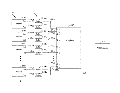
[0013] FIG. 2 is a notional representation of a miniature electronic
pressure
scanner with a voltage buffer between each pressure sensor output and
multiplexer
input according to an embodiment of the invention;
[0014] FIG. 3 is an exemplary oscilloscope trace that shows settling
times of
buffered and unbuffered output channels of a multiplexer;
[0015] FIG. 4 is a graph showing sample system performance improvement in
raw A/D count change at different temperatures of buffered and unbuffered
scanners
using an Initium data acquisition system;
[0016] FIG. 5 is a graph showing sample system performance improvement in
raw A/D counts at 80 degrees Celsius of buffered and unbuffered scanners using
an
Initium data acquisition system;
[0017] FIG. 6 is a graph showing sample system performance improvement in
raw A/D count change at 80 degrees Celsius of buffered and unbuffered scanners
using an lnitium data acquisition system;
[0018] FIG. 7 is a block diagram showing steps of a method for measuring
pressure according to an embodiment of the invention;
[0019] FIG. 8 is a topographic view of an exemplary circuit board of a
miniature electronic pressure scanner;
[0020] FIG. 9 is a schematic of an exemplary miniature electronic
pressure
scanner;
[0021] FIG. 10A is a perspective section view of an exemplary pressure
sensor and buffer arrangement of an exemplary miniature electronic pressure
7
CA 02903981 2015-09-03
WO 2014/138030 PCT/US2014/020231
scanner in which the transistor and resistor buffer elements are configured as
bare
die elements;
[0022] FIG. 10B is a perspective section view of an exemplary pressure
sensor and buffer arrangement of an exemplary miniature electronic pressure
scanner in which the transistor buffer element is configured as a bare die
element
and the resistor buffer element is integral to the sensor; and
[0023] FIG. 10C is a perspective section view of an exemplary pressure
sensor and buffer arrangement of an exemplary miniature electronic pressure
scanner in which the transistor and resistor buffer elements are both integral
to the
pressure sensor.
DETAILED DESCRIPTION
[0024] FIG. 1 is a notional representation of a miniature electronic
pressure
scanner 100 such as an ESP pressure scanner manufactured by Measurement
Specialties, Inc. Pressure Systems. Such miniature electronic pressure scanner
includes a plurality of miniature electronic differential pressure measurement
units or
pressure sensors 110A-110N, In an exemplary embodiment, this arrangement may
be configured as an array of silicon piezoresistive pressure sensors, one for
each
pressure port. The pressure sensors may be mounted on a common hybrid glass
substrate. The pressure sensors are electrically connected to multiplexer 120,
which
typically may have 16 input channels. As will be understood, the multiplexer
allows
the sensor outputs of each sensor to be addressed individually. In an
embodiment
in which there are more sensor outputs than input channels for the
multiplexer,
8
CA 02903981 2015-09-03
WO 2014/138030 PCT/US2014/020231
multiple multiplexers may be used. In an embodiment, an analog to digital
(A/D)
converter 130 may be connected to the output of the multiplexer. In another
embodiment, other electrical devices such as an amplifier may be connected to
the
output of the multiplexer. However, a problem with such a configuration is the
relatively long settling times associated with the time required for voltage
spikes
created on the multiplexed signals emanating from each miniature pressure
sensor
to decay and return the signal line to its true value.
[0025] Referring now to FIG. 2, there is shown a notional representation
of a
miniature electronic pressure scanner 200 according to an embodiment of the
disclosure and configured to mitigate the relatively long settling time
problems
associated with the configuration of FIG. 1. As shown, a plurality of
miniature
pressure sensors 210A-210N are configured such that each of the corresponding
output ports (210A01, 210A02, 210601, 210B02,
210N01, 210NO2 ) is connected to a
corresponding input of a respective buffer (labeled generally as 215). Each of
the
buffers 215 (215A1, 215A2, 21561, 215B2,.. .215N1, 215N2) is directly
connected
between each corresponding sensor output and a multiplexer 220 input port
(220A,1,
220Al2, 2206,1, 220b11,... 220N11, 220 Ni2). According to an aspect of the
present
disclosure, placing buffers between the output of each sensor and the
multiplexer
greatly improves signal settling characteristics associated with the pressure
scanner
200.
9
CA 02903981 2015-09-03
WO 2014/138030 PCT/US2014/020231
[0026] According to a further aspect of the disclosure, each miniature
buffer
215 is composed of a simple transistor common collector emitter-follower
voltage
buffer or equivalent in bare die form (i.e., unpackaged semiconductor
electrical
elements) mounted on a substrate. Use of this type of buffer in the
configuration as
shown effectively reduces the pressure sensors' bridge output impedance by
multiple orders of magnitude. The sensor or source's output impedance plays a
dominant role in the system settling time constant, and it has been discovered
that
the electronic pressure sensor analog output ¨ buffer ¨ multiplexer
configuration as
described herein dramatically improves/reduces this time constant, and
therefore
allows faster scanning or multiplexing speeds.
[0027] As described above with respect to the conventional configuration
of
FIG. 1, an embodiment of a miniature electronic pressure scanner without
sensor
buffers is a scanner such as the Measurement Specialties ESP 64HD. The
pressure
sensors used within that unit are Measurement Specialties P3377UltrastableTM
Sensors, where each of the sensors has two sensor outputs. The multiplexer may
be embodied as an Analog Devices ADG507 module, which is a packaged electrical
element, but the multiplexer may also be a bare die element without packaging.
Typically, the multiplexer will have 16 channels, and the number of
multiplexers used
will depend on the number of pressure sensors being monitored. Without a
buffer,
the output impedance of each of the sensor outputs is approximately 2500 ohms.
CA 02903981 2015-09-03
WO 2014/138030 PCT/US2014/020231
[0028] In accordance with an embodiment of the present disclosure,
configuring the system using buffer 215 at the sensor 210 output, realizes an
output
impedance (as seen from the input of multiplexer 220) of as low as 20 ohms,
representing a reduction of the output impedance of more than two orders of
magnitude. In an embodiment, each buffer 215 of the array of buffers may be
embodied as a 2N3904 transistor manufactured by Central Semi and 2000 ohm bias
resistor from Mini-Systems Inc. Such a buffer arrangement has been observed to
provide an approximate 20 ohm output resistance for the sensor. The unique
configuration of employing a voltage buffer on each output node of a pressure
sensor for sensor arrays to improve signal settling results in a very small,
simplistic
electronic voltage buffer that greatly improves the output impedance of the
sensor
output and the associated system electronics. Thus, buffering of the sensor
outputs
is performed in a manner that is economical and requires minimal component
real
estate. An additional feature of this design is that including the buffer
reduces the
common mode voltage bias level by the amount of the transistor emitter voltage
drops. This reduction in the sensor's common mode voltage has beneficial
performance implications for the upstream amplifier and/or other electronics.
[0029] The transistor and bias resistor buffer may be implemented in
different
configurations to form a voltage buffer. Transistors types may include bipolar
junction transistors (BJTs), field-effect transistors (FETs), metal oxide
semiconductor
field-effect transistors (MOSFETs), insulated-gate bipolar transistors
(IGBTs), and
other types of transistors with simple resistive biasing network. In an
embodiment,
11
CA 02903981 2015-09-03
WO 2014/138030 PCT/US2014/020231
the transistor and resistor are configured as bare die elements (electrical
elements
without packaging) that are mounted or affixed to an open area of the circuit
board
substrate to which the sensors and multiplexers are mounted. Each transistor
and
resistor may then be electrically connected to a sensor output using bond
wires, or
using circuit traces if the circuit board has been configured to support the
transistor
and resistor.
[0030] In another embodiment, the transistor and resistor may be
integrated
into the substrate of the pressure sensor die of the sensor whose sensor
output(s)
are being buffered, in which case bare die transistor and resistors will not
have to be
included on the circuit board substrate as described above. In another
embodiment,
the buffer may be comprised of a bare die transistor mounted on the circuit
board
substrate, and a resistor that is integral to the pressure sensor. A sensor
die may
typically include an unused resistor (a resistor within the sensor that is not
used to
implement the sensor's sensing functions) which may be used to bias the
transistor,
thereby eliminating the need to integrate an additional bare die resistor onto
the
circuit board substrate. As will be understood, the size of the transistors
and
resistors used may depend on the particular scanner being used, the available
space for those components in either bare form on the circuit board or
integrated
within the pressure sensor die, and the desired output impedance. In an
embodiment in which a plurality of sensor outputs are being buffered, a
plurality of
buffers are needed, and the plurality of buffers will include a plurality of
buffer
transistors and bias resistors. The term buffer as used herein generally
refers to a
12
CA 02903981 2015-09-03
WO 2014/138030 PCT/US2014/020231
single transistor and single resistor coupled to a single sensor output,
however, a
buffer may alternatively refer to more than one set of transistors and
resistors, such
as a buffer that buffers both (or more) of the outputs of a given pressure
sensor. For
example, a buffer that buffers two sensor outputs on a sensor will include two
transistors and two bias resistors.
[0031] Still referring to FIG. 2, the analog output signal (indicated
generally as
SA) provided by each of the sensor outputs is passed through a corresponding
buffer 215 to the multiplexer 220. That is, each output signal from each
sensor
output may be termed an analog output pressure signal (SA01, SA02, BBoi, BB02,
SNoi, SN02 ) indicative of the pressure detected by the pressure sensor
element
associated with the various locations on a test member. Each sensor output
signal
that is passed through a buffer 215 may be termed a buffered analog output
signal
(BA01, BA02, BBoi, BB02, BNoi, BN02 ) and representing the analog output
pressure signal, but having at least a reduced output impedance as seen from
the
input of the multiplexer 220. As noted, where the number of sensors being read
exceeds the number of input channels for the multiplexer, more than one
multiplexer
may be used. In an example, if one hundred sensors 210 are being monitored,
and
each sensor has two sensor outputs, then the system would have two hundred
sensor outputs to multiplex. In this embodiment, at least thirteen (13)
sixteen
channel multiplexers would be needed to receive the two hundred outputs of the
one
hundred sensors. In an embodiment in which each output is buffered, two
hundred
buffers would be needed, one for each of the sensor outputs. In other
embodiments
13
CA 02903981 2015-09-03
WO 2014/138030 PCT/US2014/020231
(not shown), it is possible that not every output would be buffered. For
example, in
an exemplary embodiment only one of the outputs on each of the sensors would
be
buffered (i.e., resulting in half of the total outputs being monitored). In
this
embodiment, it is conceivable that strategies directed to the order in which
buffered
and unbuffered outputs are addressed could be used to minimize settling time
limitations caused by the unbuffered outputs. As will be understood, however,
from
a performance standpoint, buffering of every sensor output would result in a
system
with the least potential for experiencing settling time problems.
[0032] FIGS. 3 and 4 illustrate the significant improvement in switching
times
realized by embodiments of the invention, relative to conventional unbuffered
pressure scanning. Specifically, FIG 3 is an exemplary oscilloscope trace 300
that
shows settling times of buffered and unbuffered channels on an ESP 64HD
pressure
scanner. As shown in FIG. 3, line 310 represents the unbuffered channel and
shows
that because of the voltage spike attributable to the multiplexer, the signal
takes
more than 60 microseconds to settle to a state in which it is readable at
point P1. In
contrast, line 320 represents a channel to which a buffer was added. As shown,
line
320 settles within 10 microseconds (approx. 8 microseconds after spiking) at
point
P2. The quick switching time of the buffered sensor greatly increases the rate
at
which individual sensors may be scanned by the multiplexer. Implementing a
pressure scanner with buffered sensor outputs as described herein allows the
multiplexer to have a switching rate of 50 microseconds per output channel. As
shown by line 320, it may be possible to achieve a faster multiplexer
switching time
14
CA 02903981 2015-09-03
WO 2014/138030 PCT/US2014/020231
such as 10 microseconds per output channel with appropriate buffering to
reduce
the settling time of the multiplexer voltage spikes.
[0033] In an embodiment, the output of the multiplexer of the scanner
systems
shown in FIGs. 2 and 3 may be electrically connected to an analog to digital
(A/D)
converter to provide a digital output of each sensor output reading. Counts
may be
made of the output of the A/D converter, which are indicative of how many
sensor
output readings are observed from the ND output. Raw A/D counts may be made of
buffered and unbuffered output channels to assess the performance of those
output
channels under different operating conditions. In FIG 4., a graph 400 shows
sample
system performance improvement of the electronic pressure scanner in raw A/D
(analog to digital) counts for a given data acquisition system. The data
acquisition
system collects the change in raw A/D counts from scanning speeds from 80
microseconds (80uS) to 26uS. Data was also collected at different temperature
conditions, at 23 degrees Celsius (C) and the other at 80 degrees Celsius. As
indicated in FIG. 4, channels 2, 3, and 4 were buffered (using a single
transistor
emitter-follower arrangement as described herein), channels 9-16 were not
used,
and channels 17-64 were unbuffered.
[0034] As shown in FIG. 4, higher ambient temperatures result in an
increase
in the A/D count change. This is at least in part because the higher
temperatures
increase the settling time for the multiplexers, with the increased settling
time
resulting in a lower number of counts and, hence, an increased change in the
CA 02903981 2015-09-03
WO 2014/138030 PCT/US2014/020231
number of counts. Thus, as shown in FIG. 4, the count change (i.e., the change
in
the number of counts) was much higher at 80 Celsius (reflected in line 420)
than 23
C (reflected in line 410), for both the buffered and unbuffered output
channels. At
either temperature, a significant improvement is seen on the buffered output
channels compared to the unbuffered output channels. The count changes of the
unbuffered output channels are represented by a large saw-tooth pattern
indicative
of a drastic fluctuation in the number of A/D counts, indicating that the
number of
sensor readings changed drastically because of the long settling times
associated
with the unbuffered output channels. In contrast, the buffered output channels
showed a much less drastic change in A/D count performance, indicating that
the
number of sensor output readings made did not change as much because of the
short settling times of the buffered output channels. This A/D system utilizes
a +/-
5-volt signal swing for 16-bit range operation, which results in approximately
0.003%
fullscale bit weight per count. As shown in FIG. 4, the 80 celsius scanning
error
comparing 26 microsecond to 80 microsecond scanning times of the unbuffered
sensor outputs is approximately 50 counts or 0.15% fullscale error, while the
same
scanning of buffered sensor outputs results in errors close to the systems
resolution
limit. Even at 23 celsius, comparing the same 26 microsecond to 80 microsecond
scanning times, the unbuffered sensor output A/D count error is still
approximately
counts or 0.03% fullscale, while the buffered sensor output error is not
perceivable.
16
CA 02903981 2015-09-03
WO 2014/138030 PCT/US2014/020231
[0035] FIG. 5 shows a graph 500 of sample system performance
improvement of the electronic pressure scanner in raw A/D (analog to digital)
counts
at different acquisition speeds and temperatures, for a given data acquisition
system. FIG. 5 graphs the A/D counts of an unbuffered output at 83
microseconds
scanning speed, an unbuffered output at 26 microseconds scanning speed, a
buffered output at 83 microseconds scanning speed, and a buffered output at 26
microseconds scanning speed. As in FIG. 4, the buffered channels 530 and 540
of
FIG. 5 illustrate significant improvement in performance over their unbuffered
counterparts 510 and 520, respectively. In particular, FIG. 5 shows that the
buffered output lines 530 and 540 operate very similarly (as shown by the
graph
lines essentially tracking one another) at different scanning speeds of 26 and
83
microseconds. In contrast, unbuffered output lines 510 and 520 show a
separation
between them, indicating that the unbuffered lines experience a discernible
difference in performance at different scanning speeds. As discussed herein,
this
difference in performance is attributable to factors such as voltage spikes
that cause
long settling times in unbuffered output lines.
[0036] FIG. 6 is a graph 600 showing sample system performance
improvement of the electronic pressure scanner in A/D (analog to digital)
count
changes for buffered and unbuffered outputs, using a given data acquisition
system.
The data acquisition system collected the change in raw A/D counts from
scanning
speeds from 80uS to 26uS. As shown in graph 600, the line representing the
unbuffered output 610 shows a marked sawtooth pattern, which is indicative of
17
CA 02903981 2015-09-03
WO 2014/138030 PCT/US2014/020231
settling time limitations associated with unbuffered outputs. In contrast,
line 620
representing the buffered outputs shows a fairly flat A/D count change,
indicating
that the change in scanning speeds has a much smaller effect, if any, on A/D
count
change of the buffered outputs.
[0037] FIG. 7 is a simplified logic flow chart or diagram illustrating
processing
steps according to aspects of the disclosure. At block 710, pressure is sensed
using
a plurality of miniature pressure sensors associated with various locations on
a body
for sensing pressure thereon. Each pressure sensor has one or more outputs and
generates one or more analog output signals representative of the sensed
pressure.
Each sensor output also has an associated output impedance. At block 720, one
or
more of the sensor outputs using a buffer that is electrically coupled to the
output
port of the sensor and to an input port of a multiplexer. Each buffer is
operative to
pass through the analog output pressure signal of the sensor output coupled
thereto,
and configured to reduce the output impedance of the sensor output coupled to
it.
As discussed, the buffer may comprise a bipolar junction transistor and a bias
resistor. At block 730, the buffered output pressure signals from the sensor
outputs
are multiplexed, using a multiplexer. A typical multiplexer may have 16 input
channels, although other configurations (e.g., 8 channel or 32 channel) may
also be
used. As will be understood, a multiplexer allows all of the output signals to
be
routed to a single receiving device, such as an A/D converter, which
eliminates the
need to have a separate receiving device for each output line. As noted, wind
aerodynamics applications may have a thousand or more sensors, thereby
18
CA 02903981 2015-09-03
WO 2014/138030 PCT/US2014/020231
eliminating the need for multiple receiving devices such as A/D converters and
resulting in substantial savings both in terms of space and cost. Finally at
block 740,
switching is performed between channels of the multiplexer, thereby
selectively
reading the buffered output(s) of each of the miniature pressure sensors. A
computer processor and associated logic may be used to cause the multiplexer
to
switch between channels. Because the buffer between the sensor outputs and
multiplexer greatly reduces the settling time of the multiplexer channels, the
timing of
the switching can be much faster than without the buffer.
[0038] FIG. 8 is a topographical view of a portion of an exemplary
circuit
board of a miniature electronic pressure scanner 200 as represented for
example, in
FIG. 2. The embodiment of FIG. 8 depicts a scanner 800 that includes pressure
sensors labeled generally as 820 electrically coupled to multiplexers labeled
generally as 840 via, buffers labeled generally as 830. In the configuration
shown in
FIG. 8, 16 each of pressure sensor elements (8201, ..., 82016) is associated
with a
respective channel (e.g. CH1, ..., CH16) and provides two analog outputs.
Coupled
to each pressure sensor analog output is a corresponding buffer bias
transistor (e.g.
83081 and 83082 for pressure sensor 8208 of CH8) where in the embodiment
shown,
the associated buffer resistors are integral to the sensor 820. Multiplexers
840 are
also disposed on substrate 810. FIG. 8 also depicts locations 850 for trim
resistors,
locations 860 for span compensation resistors, and wire bond pads 870 to
connect
each pressure sensor to the substrate 810. In an exemplary embodiment, a
miniature pressure sensor 820 may be a square semiconductor element in which
19
CA 02903981 2015-09-03
WO 2014/138030 PCT/US2014/020231
each side (dimension A on FIG. 8) is approximately .074 inches in length and
the
bare die transistor 830 may be an unpackaged semiconductor element having
sides
with lengths of approximately .015 inches (dimension B) x .018 inches
(dimension
C).
[0039] As depicted in FIG. 8, the array of miniaturized pressure sensors
820
is configured such that each sensor output is buffered by a bare die
transistor 830
for each output (hence each sensor 820 has two bare die transistors next to it
on or
adjacent to) the substrate). The bias resistor for each output is within or
integral to
each sensor element 820 and hence not shown. In other embodiments, the bias
resistor may be a separate bare die resistor for each buffer on the substrate.
As
shown, buffer transistor 830 is only a fraction of the size of the pressure
sensor
element 820, and the ratio of the area of the bare die buffer transistor to
the area of
the sensor is very small, with the buffer transistor being less than about 5%
(e.g.
approximately 4.9%) of the area of the sensor.
[0040] As will be understood, in an embodiment in which the bias resistor
is a
bare die element mounted on the substrate rather than integral to the pressure
sensor, the ratio of the area of the bare die buffer elements to the sensor
will be
larger than about 4.9% because of the addition of the bare die resistor, and a
topological view of this embodiment would include a bare die element for the
resistor
mounted on the substrate. Nevertheless, because the bare die resistor is
typically
smaller than the bare die transistor, the ratio of the area of the bare die
buffer
CA 02903981 2015-09-03
WO 2014/138030 PCT/US2014/020231
transistor and bare die resistor combination will be less than about 10% of
the area
of the sensor (the sensor area being unchanged from the integral embodiment).
In
an embodiment in which both the transistor and bias resistor that make up the
buffer
are part of and integral to the sensor element 820, a topological view of such
embodiment would not include either a bare die transistor or bare die resistor
next to
(adjacent) each sensor. Thus, the integrated pressure sensor and buffer
configuration provides for the requisite functionality having reduced area
relative to
the aforementioned embodiments.
[0041] FIG. 9 is a schematic illustration of a portion of an exemplary
miniature
electronic pressure scanner 900 which depicts two buffered pressure sensors
920,
925. Pressure sensor 920 includes analog pressure sensor outputs SO1 and S02.
Sensor 925 includes analog sensor outputs S03 and SO4. In the exemplary
embodiment of FIG. 9, each of the sensor outputs is buffered by a transistor
(Q) and
a bias resistor (R). Transistor Q1 and resistor R1 buffer sensor output 501,
and
provide a buffered output B01 to the multiplexer 940. Similarly, transistor Q2
and
resistor R2, transistor Q3 and resistor R3, and transistor Q4 and resistor R4
bias
sensor outputs S02, S03, and SO4, respectively. Buffered outputs B02, B03, and
B04, respectively, are provided to multiplexer 940. The pressure sensors 920
and
925 may include trim and compensation resistors (not shown) as discussed with
respect to the topological embodiment shown in FIG. 8. Multiplexer 940
includes
outputs MO1 and M02, which may output to an amplifier or A/D converter or
other
electrical device (not shown). As will be understood, the schematic of FIG. 9
is
21
CA 02903981 2015-09-03
WO 2014/138030 PCT/US2014/020231
representative of a buffer configuration which may be used when the resistor
and
transistor buffer elements are bare elements, or when one or both of the
buffer
elements are integrated into the pressure sensor.
[0042] FIGs. 10A, 10B, and 10C, respectively illustrate three embodiments
of
the pressure sensor and buffer configurations as described herein for
implementation in a pressure scanner according to aspects of the present
disclosure. As shown in FIGs. 10, 10B, and 100, like reference numerals are
used
to indicate like parts. FIG. 10A provides a perspective section view of an
exemplary
pressure sensor of a miniature electronic pressure scanner in which the
transistor
and resistor buffer elements are bare die elements. FIG. 10B provides a
perspective
section view of an exemplary pressure sensor of a miniature electronic
pressure
scanner in which the transistor buffer element is a bare die element and the
resistor
buffer element is integral to the sensor. FIG. 10C provides a perspective
section
view of an exemplary pressure sensor of a miniature electronic pressure
scanner in
which the transistor and resistor buffer elements are both integral to the
sensor.
[0043] Specifically, FIG. 10A shows substrate 1000 on which pressure
sensor
1010 is mounted. The pressure sensor 1010 analog output is buffered by bare
die
transistor 1020 and bare die bias resistor 1030, providing buffered output(s)
1060.
The pressure sensor 1010 includes circuitry, as illustrated by bridge circuit
1040
disposed atop the sensor. As will be understood by those in the art, the
circuit is an
illustration of the circuitry within the sensor and known integrated circuit
technology
22
CA 02903981 2015-09-03
WO 2014/138030 PCT/US2014/020231
may be used to implement the sensor circuitry within the sensor. For example,
the
pressure sensor may be a silicon based piezoresistive sensor having a micro-
machined diaphragm onto which four (4) piezoresistors have been diffused. The
piezoresistors are connected in a Wheatstone bridge configuration that
generates a
voltage output proportional to the pressure input, as is understood in the
art. Wire
jumpers 1050 from the sensor are used to electrically connect the bare die
transistor
1020 and bias resistor 1030 to the sensor so the outputs of the sensor may be
buffered.
[0044] FIG. 10B depicts an embodiment wherein the pressure sensor 1010 is
buffered by bare die transistor 1020 adjacent sensor 1010 and wherein resistor
1032
is integral to the sensor. The bias resistors are shown schematically on the
sensor
for illustration purposes and may be functionally integrated into the sensor
using
known integrated circuit techniques. The sensor may include unused resistors
that
may be used to bias the transistor 1020, or additional resistors (ones not
used for
the sensor circuitry) may be integrated within the sensor so that they may be
used
with the buffer transistor 1020. Wire jumpers 1050 from the sensor are used to
electrically connect the bare die transistor 1020 to the bias resistor 1032
integrated
within the sensor, and also to provide buffered output(s) 1060. In another
embodiment (not shown), the transistor for the buffer may be integral to the
sensor
circuitry and the bias resistor may be a bare element disposed on the
substrate that
is connected to the sensor using wire jumpers.
23
CA 02903981 2015-09-03
WO 2014/138030 PCT/US2014/020231
[0045] FIG. 10C depicts another embodiment showing pressure sensor 1010
mounted on a substrate and in which the transistor and bias resistor buffer
elements
are integrated onto the pressure sensor. Specifically, FIG. 10C shows a
schematic
illustration of transistor 1022 and resistor 1032 arranged with bridge circuit
1040 on
the sensor 1010. As noted, the schematic is an illustration of the circuitry
encompassed within the sensor using known integrated circuit technology is
used to
implement the sensor circuitry and buffer elements (transistor and resistor)
within the
sensor. Wire jumpers 1050 are used to electrically connect the sensor,
transistor,
and bias resistor on the sensor to the buffered output(s) 1060.
[0046] The disclosed method described herein may be automated by, for
example, tangibly embodying a program of instructions upon a computer readable
storage media capable of being read by a machine capable of executing the
instructions. A general purpose computer is one example of such a machine, as
are
other known computing devices having processors, memory, hardware, software,
and/or firmware. A non-limiting exemplary list of appropriate storage media
well
known in the art would include such devices as a readable or writeable CD,
flash
memory chips (e.g., thumb drives), various magnetic storage media, and the
like.
[0047] While the foregoing invention has been described with reference to
the
above-described embodiment, various modifications and changes can be made
without departing from the spirit of the invention. Accordingly, all such
modifications
and changes are considered to be within the scope of the appended claims.
Accordingly, the specification and the drawings are to be regarded in an
illustrative
24
CA 02903981 2015-09-03
WO 2014/138030 PCT/US2014/020231
rather than a restrictive sense. The accompanying drawings that form a part
hereof,
show by way of illustration, and not of limitation, specific embodiments in
which the
subject matter may be practiced. The embodiments illustrated are described in
sufficient detail to enable those skilled in the art to practice the teachings
disclosed
herein. Other embodiments may be utilized and derived therefrom, such that
structural and logical substitutions and changes may be made without departing
from the scope of this disclosure. This Detailed Description, therefore, is
not to be
taken in a limiting sense, and the scope of various embodiments is defined
only by
the appended claims, along with the full range of equivalents to which such
claims
are entitled.
[0048] Such embodiments of the inventive subject matter may be referred
to
herein, individually and/or collectively, by the term "invention" merely for
convenience and without intending to voluntarily limit the scope of this
application to
any single invention or inventive concept if more than one is in fact
disclosed. Thus,
although specific embodiments have been illustrated and described herein, it
should
be appreciated that any arrangement calculated to achieve the same purpose may
be substituted for the specific embodiments shown. This disclosure is intended
to
cover any and all adaptations of variations of various embodiments.
Combinations
of the above embodiments, and other embodiments not specifically described
herein, will be apparent to those of skill in the art upon reviewing the above
description.