Note: Descriptions are shown in the official language in which they were submitted.
CA 02904413 2015-09-04
WO 2014/164309 PCT/US2014/021823
SPECIFICATION
TITLE OF THE INVENTION
TRACKING POWER SUPPLY WITH INCREASED BOOST CAPABILITY
RELATED APPLICATION INFORMATION
[0001] This application claims the benefit of U.S. Application Serial No.
13/797,473,
filed on March 12, 2013, hereby incorporated by reference as if set forth
fully herein.
BACKGROUND OF THE INVENTION
1. Field of the Invention
[0002] The field of the present invention relates to power amplification
and, more
specifically, to apparatus and methods for amplifying electronic signals such
as audio signals.
2. Background
[0003] With a conventional power amplifier, the maximum available output
power is
generally limited by at least two factors: the voltage swing available at the
amplifier's output,
and the load impedance. The voltage swing is itself typically limited by the
amplifier rail
voltage. In the case of a car audio amplifier for instance, the rail voltage
is the nominal 14.4
Volts of the car battery; thus, if the amplifier were able to swing all the
way up to the power
rails, it could deliver ¨7 Volts peak output. This peak voltage is only
sufficient to deliver about
3 Watts of power to an 8E2 load. To obtain greater output power, the load
impedance can be
CA 02904413 2015-09-04
WO 2014/164309 PCT/US2014/021823
reduced (for example, a 1E2 load would allow 25 Watts of output power), but in
order not to
encounter significant losses in the wiring, the cables need to be thicker and
heavier.
[0004] In general, lowering the load impedance on an amplifier will
increase the current
that has to be supplied by the amplifier and increase the amplifier distortion
as well as requiring
more expensive output devices. Thus, merely lowering the load impedance by
itself may not
provide additional power. It would therefore be advantageous to be able to
increase the voltage
output available from the amplifier so that, for example, a higher load
impedance can be
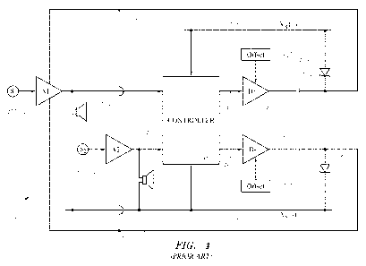
employed and/or greater power be delivered to a load.
[0005] One technique for increasing output voltage is known as bridging,
whereby two
anti-phase amplifiers are used with the load tied between their outputs. This
approach can
double the available output swing and for a given load impedance, which would
quadruple the
output power. Even so, the maximum available power to a 1E2 load, using the
typical power
supply conditions described above, would be limited to approximately 100
Watts, and would still
have the complication of a low impedance load. However, this simplified
analysis hides the fact
that under these conditions, each amplifier is not only having to supply twice
the output current
as compared to the non-bridged condition, but also sees half the effective
load impedance. In
practical applications, the amplifiers may not be able to supply the required
current.
[0006] A more valid comparison might be to calculate the maximum output
that can be
achieved for a given maximum output current capability. In the case of the
bridge amplifier, the
load impedance would therefore be double that used for the single amplifier
example. With
twice the load resistance, the power into the load is only twice that of the
single amplifier. The
effective load impedance seen by each half of the bridge amplifier is now the
same as the single
- 2 -
CA 02904413 2015-09-04
WO 2014/164309 PCT/US2014/021823
amplifier example and given that the load current sourced by the amplifier is
the same, then the
amplifier distortion is the same also.
[0007] For applications in which the amplifier is driving a speaker load
for audio sound
reproduction, the bridge amplifier could be replaced by two single amplifiers,
each driving one
of a pair of voice coils on a dual voice coil loudspeaker. The overall output
level from the
loudspeaker would then be identical for the bridge amplifier and the two
single amplifiers.
[0008] Another technique to increase effective power output is to employ
a switching
power supply to raise the power supply voltage to the amplifier. The amplifier
output voltage
capability is thereby increased, allowing a higher load impedance to be used
for a given output
current capability. This approach can mitigate the need for a low load
impedance. However, a
switching power supply typically operates at high frequency and high power and
needs careful
design to avoid interference.
[0009] Another technique, which has been employed, for example, by
Philips
Semiconductors of Eindhoven, the Netherlands, in its TDA1560/1562 products,
involves an
amplifier system that modulates its own supply voltage in order to provide a
higher output
voltage swing. A bridge amplifier is used in conjunction with a capacitive
booster circuit that
lifts the supply to approximately twice the steady-state level when a larger
output voltage swing
is required. Under quiescent conditions, the output of each amplifier in the
bridge sits at
approximately half the battery voltage. As the output of one half of the
bridge amplifier
approaches the positive supply rail, the booster circuit begins to lift the
supply voltage so that the
amplifier does not clip. However, at the same time, the output of the other
half of the bridge
amplifier approaches ground. The output can go no lower than ground potential,
and so the
amplifier system adds the difference between the actual negative going output
and the desired
- 3 -
CA 02904413 2015-09-04
WO 2014/164309 PCT/US2014/021823
negative going output to the positive going output at the other side of the
bridge amp. This
operation can result in significantly distorted waveforms at each individual
output of the bridge
amplifier, but the output measured differentially across the two outputs is
generally linear (within
the limitations of the correction circuitry). The booster circuit adjusts to
maintain sufficient
headroom above this modified output waveform. Thus the bridge amplifier output
is able to
increase sufficiently to give a peak output voltage close to twice the battery
voltage, at the
expense that this technique can generally only be used in bridge amplifier
mode.
[0010] While the foregoing approaches may increase the effective output
capability of an
amplifier, they still have appreciable limitations. It would therefore be
advantageous to provide
an improved audio amplification apparatus or method which overcomes one or
more of the
foregoing problems or limitations, provides increased power output when
needed, and/or
provides other benefits and advantages.
[0011] Another approach that has been developed for providing temporary
increased
power output when needed is disclosed in U.S. Patent 7,834,702, entitled
"Efficient Power
Amplifier," assigned to the assignee of the present invention. That patent
generally describes a
variety of embodiments of a tracking power supply that temporarily raises the
power rails to an
amplifier when the output voltage approaches the nominal rail value. While
this patent
represents an improvement over the state of the art in a variety of respects,
there may be
situations where even greater voltage levels are required.
[0012] It would therefore be advantageous to provide an improved audio
amplification
apparatus or method which has an ability to provide greater voltage boosts
when needed. It
would further be advantageous to provide an efficient audio amplification
apparatus or method
- 4 -
CA 02904413 2015-09-04
WO 2014/164309 PCT/US2014/021823
which provides increased power output without the need for a bridge amplifier
or a switching
power supply.
- 5 -
CA 02904413 2015-09-04
WO 2014/164309 PCT/US2014/021823
SUMMARY OF THE INVENTION
[0013] Certain embodiments disclosed herein are generally directed, in
one aspect, to a
power boost circuit for an amplification system. The power boost circuit
receives, as an input,
an output signal from an amplifier receiving a power supply input voltage
signal from a power
supply rail. The power boost circuit tracks the output signal from the
amplifier and temporarily
boosts the power supply input voltage signal feeding the amplifier up to some
multiple of the
nominal power rail voltage, by drawing current from one or more cascaded power
boost circuits
each including a stored energy source such as a reservoir capacitor or
battery, when the output
signal from the amplifier approaches the power supply rail voltage within a
predetermined
threshold. The power boost circuit may continuously maintain the power supply
input voltage
signal above the power supply rail voltage by the amount of the predetermined
threshold.
[0014] In another aspect, an amplification system has independent
positive and negative
power supply rail boost capability through a first cascaded power boost
circuit and a second
cascaded power boost circuit which each receive, as an input, an output signal
from an amplifier
to be supplied. The first cascaded power boost circuit and said second
cascaded power boost
circuit are selectively engaged to temporarily boost positive and negative
power supply input
voltage levels to the amplifier as the output signal from said amplifier
approaches or exceeds a
positive power supply rail or a negative power supply rail, respectively.
[0015] In yet another aspect, a dynamic amplification system for
providing power to a
plurality of amplifiers includes a first power boost amplifier system
electrically connected to a
first power supply rail and a second power boost amplifier system electrically
connected to a
second power supply rail. A power boost control circuit monitors output signal
levels from the
- 6 -
CA 02904413 2015-09-04
WO 2014/164309 PCT/US2014/021823
plurality of amplifiers and provides power boost control signals to the power
boost amplifier
systems. As a result, the first power boost amplifier system temporarily
boosts the first power
supply rail above a first nominal voltage level in tandem with the highest
output signal level
from the amplifiers, and the second power boost amplifier system temporarily
lowers the second
power supply rail below a second nominal voltage level in tandem with the
lowest output signal
level from said amplifiers. In certain embodiments, the first power boost
amplifier system may
draw current from a first plurality of stored energy sources (such as
reservoir capacitors or
batteries, or hybrids such as super-capacitors or ultra-capacitors) when
active to boost the first
power supply rail above the first nominal voltage level, and, similarly, the
second power boost
amplifier system may draw current from a second plurality of stored energy
sources (such as
reservoir capacitors or batteries, or hybrids such as super-capacitors or
ultra-capacitors) when
active to lower the second power supply rail below the second nominal voltage
level.
[0016] In yet a further aspect, an tracking power supply for an
amplification system has
an independent positive power supply rail boost capability through a cascaded
first and second
positive power boost circuit, and an independent negative power supply rail
boost capability
through a cascaded first and second negative power boost circuit. Each power
boost circuit
receives, as an input, an output signal from an amplifier to be supplied. The
first positive power
boost circuit and second positive power boost circuit are selectively engaged
to temporarily
boost positive supply input voltage levels to the amplifier as the output
signal from said amplifier
approaches or exceeds a positive power supply rail. The first negative power
boost circuit and
second negative power boost circuit are selectively engaged to temporarily
boost negative supply
input voltage levels to the amplifier as the output signal from said amplifier
approaches or
exceeds a negative power supply rail.
- 7 -
CA 02904413 2015-09-04
WO 2014/164309 PCT/US2014/021823
[0017] Further embodiments, variations and enhancements are also
disclosed herein.
BRIEF DESCRIPTION OF THE DRAWINGS
[0018] FIG. 1 is diagram of a single-channel power amplifier including
power rail boost
circuitry as known in the art.
[0019] FIG. 2 is a diagram of a dual-channel power amplifier including
power rail boost
circuitry as known in the art.
[0020] FIG. 3 is a graph illustrating waveforms relating to an example of
operation of the
power amplifier of FIG. 2.
[0021] FIG. 4 is a more detailed diagram of a particular power amplifier
including power
rail boost circuitry, in accordance with various principles illustrated in or
discussed with respect
to FIG. 2.
[0022] FIG. 5 is a diagram of another example of a single-channel power
amplifier
including power rail boost circuitry as known in the art.
[0023] FIG. 6 is a diagram of an example of a dual-channel power
amplifier including
power rail boost circuitry as known in the art.
[0024] FIG. 7A is a diagram of another example of a single-channel power
amplifier
including power rail boost circuitry as known in the art, and which adjusts
for decay or droop,
and FIG. 7B depicts a variation of the amplifier of FIG. 7A which includes
circuitry for sensing a
difference between the supply voltage and an amplified version of the main
amplifier input in
order to drive the feedback loop.
- 8 -
CA 02904413 2015-09-04
WO 2014/164309 PCT/US2014/021823
[0025] FIG. 8A is a diagram of a dual-channel power amplifier including
power rail
boost circuitry as known in the art, which adjusts for decay or droop, and
FIG. 8B depicts a
variation of the amplifier of FIG. 8A which includes circuitry for sensing a
difference between
the supply voltage and an amplified version of the main amplifier input to
drive the feedback
loop.
[0026] FIG. 9 is a diagram of an embodiment of an N-channel power
amplifier including
power rail boost circuitry as known in the art.
[0027] FIG. 10 is a block diagram of an embodiment of a tracking power
supply with
cascaded power boost circuitry, for use in conjunction with, e.g., a power
amplifier.
[0028] FIG. 11 is a diagram illustrating a tracking power supuply with
cascaded power
boost rail circuitry in accordance with the principles illustrated in FIG. 10,
according to one
embodiment as disclosed herein.
[0029] FIG. 12 illustrates a set of graphs illustrating an example of
certain voltage
waveforms and relationship pertaining to operation of the power boost
circuitry of FIG. 11.
[0030] FIG. 13 is a circuit schematic diagram illustrating one possible
implementation of
the tracking power supply illustrated in FIG. 11.
[0031] FIG. 14A is a diagram showing an example of an N-channel power
amplifier
including cascaded power rail boost circuitry according to one embodiment as
disclosed herein.
[0032] FIG. 14B is a diagram showing an example of an N-channel power
amplifier
including cascaded power rail boost circuitry according to another embodiment
as disclosed
herein, where the output of a first power boost stage is coupled to the
downstream power boost
stage.
- 9 -
CA 02904413 2015-09-04
WO 2014/164309 PCT/US2014/021823
[0033] FIG. 15 is a circuit schematic diagram illustrating a tracking
power supply with
cascaded power boost circuits according to another embodiment as disclosed
herein.
[0034] FIG. 16 is a block diagram of an alternative embodiment of a
tracking power
supply with cascaded power boost circuitry, where the output of each power
boost stage is
coupled to an input of the downstream power boost stage.
[0035] FIG. 17 illustrates a set of graphs illustrating an example of
certain voltage
waveforms and relationship pertaining to operation of the power boost
circuitry of FIG. 15.
DETAILED DESCRIPTION OF PREFERRED EMBODIMENTS
[0036] Certain embodiments disclosed herein are generally directed, in
one or more
aspects, to a power boost system or circuit which tracks an amplifier input or
output signal and
temporarily boosts the power supply voltage signal feeding the amplifier when
required by the
needs of the amplifier output signal. At least some of these embodiments are
designed to enable
a larger peak-to-peak voltage swing of, e.g., over three times the supply or
battery voltage,
without necessarily the use of a bridged amplifier configuration or the need
for a high frequency
switching power supply. Some of these embodiments may also provide for greater
efficiency
than a standard amplifier configuration, especially with audio signal
amplification, thereby
reducing heat-sinking requirements. The high output voltage swing also may, in
at least some
cases, permit a relatively normal load impedance to be used.
[0037] According to various embodiments as disclosed herein, a tracking
power supply
for an amplifier includes one or more cascaded sets of power boost circuits
configured to
temporarily boost positive and/or negative power supply rails. Each power
boost circuit may
- 10 -
CA 02904413 2015-09-04
WO 2014/164309 PCT/US2014/021823
include a gain element and a stored energy source (such as a capacitor or
battery), and the power
boost circuits are linked in a cascade fashion to provide a greater degree of
voltage boost when
needed. An optional control circuit monitors amplifier output signal levels,
or separately
amplified input signal levels, and provides power boost control signals to the
power boost
circuits, which temporarily raise or lower the positive and/or negative supply
voltages above or
below the nominal voltage rails in tandem with the highest and lowest output
signals,
respectively, from the amplifier(s).
[0038] Embodiments as disclosed herein may be employed in a variety of
applications,
and may be particularly well suited for situations in which it is desired to
attain a temporary
boost in output power. In particular, various embodiments as described herein
may be well
suited for audio amplification systems which may operate mostly within the
bounds of the
nominal voltage rails but occasionally require peak voltage swings that exceed
the nominal
voltage rails.
[0039] FIG. 1 is a high-level diagram of a single-channel power
amplification system
100 as known in the art, and as generally described in detail in U.S. Patent
7,834,702, assigned to
the assignee of the present invention, and incorporated by reference as if set
forth fully herein.
In FIG. 1, a main amplifier 104 (denoted "Al") amplifies a source signal 102.
The main
amplifier 104 may be of any conventional design, although it preferably has a
high power supply
rejection ratio (PSRR). The main amplifier 104 in this example is connected to
a loudspeaker
150, optionally through a coupling capacitor 115 ("C3"), in a conventional
manner. The main
amplifier 104 is coupled to the power supply lines 128 (Vs+) and 138 (Vs-)
through diodes 129
("Dl") and 139 ("D2"), respectively. Diodes 129 and 139 may be Schottky type
diodes so as to
provide rapid switching time and also to maximize the potential boost level.
- 11 -
CA 02904413 2015-09-04
WO 2014/164309 PCT/US2014/021823
[0040] Positive power boost amplifier 120 (denoted "B+" in part because
it pertains to
the positive supply voltage) and negative power boost amplifier 130 (denoted
"B-" in part
because it pertains to the negative supply rail) are coupled to power supply
lines 128 (Vs+) and
138 (Vs-), respectively. The positive and negative power boost amplifiers 120
and 130 are
coupled to the power supply inputs 107, 108 (denoted Vboost+ and Vboost- in
FIG. 1) of the
main amplifier 104 via reservoir capacitors 125 ("Cl") and 135 ("C2"). Offset
signal inputs 121,
131 are coupled to power boost amplifiers 120 and 130, respectively. Offset
signal 121 is
provided so that the output signal 122 from positive power boost amplifier 120
is at Vs- (the
negative supply rail) when its boost function is inactive, and offset signal
131 is provided so that
the output signal 132 is at voltage level Vs+ (the positive supply rail) when
its boost function is
inactive. As a result, the first reservoir capacitor 125 is normally fully
charged when the positive
boost function is not required, and has a voltage across it of (Vs+ - Vs- -
VD1), where VD1 is the
voltage drop across Dl. Likewise, the second reservoir capacitor 135 is
normally fully charged
when the negative boost function is not required, and has a voltage across it
of (Vs+ - Vs- -
VD2), where VD2 is the voltage drop across D2. With a 14.4V power supply, the
voltage across
each of the reservoir capacitors 125, 135 would thus typically be about 13.9
Volts.
[0041] In operation, power boost amplifiers 120 and 130 sense the output
of the main
amplifier 104, and produce output signals 122, 132 that drive the power supply
inputs 107, 108
of the main amplifier 104 via reservoir capacitors 125 ("Cl") and 135 ("C2").
Under quiescent
conditions, the DC output voltage of the main amplifier 104 to be supplied
generally lies halfway
between the positive and negative power supply rails Vs+ and Vs-. When the
required output of
the main amplifier 104 is less than the limits imposed by power supply rails
Vs+ and Vs-, the
amplification system 100 operates as a conventional amplifier. In other words,
the main
- 12 -
CA 02904413 2015-09-04
WO 2014/164309 PCT/US2014/021823
amplifier 104 draws power from the positive and negative supply lines 128, 138
via D1, D2
respectively, and the source signal 102 is amplified by main amplifier 104 in
a conventional
manner.
[0042] However, when the source signal 102 reaches amplitudes requiring
that the output
signal 105 approach or exceed the power supply rails 128 (Vs+) and/or 138 (Vs-
), the operation
of the amplification system 100 changes to allow increased power output. The
main amplifier
104 normally derives current from the power supply rails Vs+ and Vs- via
diodes D1 and D2
(129 and 139), and delivers power to the load, i.e., the loudspeaker 150.
Thus, the maximum
peak-to-peak output voltage under ordinary conditions, without the effect of
positive or negative
power boost amplifiers 120, 130, is generally given by the equation: (Vs+ - Vs-
) - (VD1 + VD2);
that is, the maximum peak-to-peak output voltage is the difference between the
positive and
negative supply rails less the voltage drops caused by diodes 129, 139. In the
amplification
system 100, as the output voltage from the main amplifier 104 approaches the
positive or
negative supply rail, power boost amplifier 120 or 130 (depending upon the
polarity of the
signal) will force a temporary increase to power supply input(s) 107 and/or
108 as needed,
allowing the main amplifier 104 to increase the amplitude of its output signal
105 and its overall
power output.
[0043] The power boost operation of amplification system 100 will now be
explained in
greater detail, taking first the example where the source signal 102 is
positive and will require a
boost in the positive power supply input 107. As the output signal 105 from
the main amplifier
104 approaches the positive supply rail Vs+ within a certain,range (typically
1.5 Volts) of Vs+,
the output 122 of power boost amplifier 120 (B+) starts to rise up from its
quiescent state, which
is at Vs- potential. In its quiescent state, power boost amplifier 120 charges
up reservoir
- 13 -
CA 02904413 2015-09-04
WO 2014/164309 PCT/US2014/021823
capacitor 125 (Cl) to a voltage of (Vs+ ¨ VD1), where VD1 is the drop in
voltage across diode
129 (D1). The rise in output signal 122 caused by the rise in main amplifier
output signal 105 is
transferred via the reservoir capacitor 125 (Cl) to the positive power supply
input 107 of the
main amplifier 104, raising its potential (Vboost+). As this occurs, diode 129
(D1) is cut off so
that the positive power supply input 107 of main amplifier 104 becomes
isolated from the
positive power supply rail Vs+ and, instead, its input current is derived from
the output of power
boost amplifier 120 (B+) via reservoir capacitor 125 (Cl). As a result, the
main amplifier output
signal 105 is no longer limited by the positive power supply rail Vs+.
[0044] If power boost amplifier 120 (B+) has, for example, unity gain,
then the voltage
level of positive power supply input 107 to main amplifier 104 tracks the main
amplifier 104's
output voltage, albeit with an offset of some amount, so that the difference
between the voltage
level of the main amplifier output 105 and its supply voltage, Vboost+, is
held relatively constant
at, e.g., approximately 1.5 Volts. Thus the output 105 of the main amplifier
104 is permitted rise
above the positive power supply voltage Vs+ while preventing saturation and/or
clipping.
[0045] This manner of operation may continue until the output 122 of
power boost
amplifier 120 reaches the positive rail voltage Vs+ and clips. The main
amplifier's positive
power supply input 107 (Vboost+) then rises no further, and the output 105 of
the main amplifier
104 can then only rise slightly higher until it too clips at a final potential
of (2Vs+ - VD1).
[0046] When the output signal 105 from main amplifier 104 swings the
other direction,
i.e., negative, then a similar effect occurs with negative power boost
amplifier 130 (B-), reservoir
capacitor 135 (C2), and diode 139 (D2). These components act in a similar
manner to the
positive supply components, but instead move the negative power supply input
108 (Vboost-)
below the potential of the negative supply rail Vs-. This manner of operation
may continue until
- 14 -
CA 02904413 2015-09-04
WO 2014/164309 PCT/US2014/021823
the output 132 of negative power boost amplifier 130 reaches the negative rail
voltage Vs- and
clips. The main amplifier's negative power supply input 108 (Vboost-) then
drops no further,
and the output 105 of the main amplifier 104 can then only drop slightly lower
until it too clips at
a final potential of (2Vs- + VD2).
[0047] It may be thus seen that both the positive and negative power
supply inputs 107
and 108 of main amplifier 104 can be independently boosted, with the positive
power supply
input 107 being boosted above the positive supply rail Vs+ and the negative
power supply input
108 being boosted below the negative supply rail Vs-. This effect provides a
large voltage swing
capability to the main amplifier 104. An amplification system 100 configured
in accordance
with FIG. 1 can be built without a bridged amplifier arrangement and without a
switching power
supply, yet still have a large voltage swing capability.
[0048] The principles of the amplification system 100 illustrated in FIG.
1 may be
extended to systems having more than one channel and/or more than one main
amplifier. An
example of one embodiment of this type as known in the art is illustrated, in
somewhat
simplified form, in FIG. 2. As shown in FIG. 2, a multi-channel amplification
system 200
includes, in this example, two main amplifiers 204, 254 (also denoted "Al" and
"A2") to be
supplied, and, as in FIG. 1, two power boost amplifiers 220, 230. The output
of the first power
boost amplifier 220 is coupled to the positive power supply inputs of both
main amplifiers 204,
254, while the output of the second power boost amplifier 230 is coupled to
the negative power
supply inputs of both main amplifiers 204, 254. In other words, the main
amplifiers 204, 254
have common power supply inputs. The first main amplifier 204 amplifies a
first input source
signal 202, and produces an output signal 205 which is provided to a
loudspeaker 250 as well as
a controller 260. Similarly, the second main amplifier 254 amplifies a second
input source signal
- 15 -
CA 02904413 2015-09-04
WO 2014/164309 PCT/US2014/021823
203, and produces an output signal 255 which is provided to another
loudspeaker 251 as well as
the controller 260.
[0049] In operation, the amplification system 200 works in a very similar
way to the
amplification system 100 of FIG. 1. However, since there are now two main
amplifiers 204,
254, the controller 260 reacts to the main amplifier 204 or 254 which requires
the greatest output,
and causes the power boost amplifiers 220, 230 to provide the required supply
voltage based
thereon. The controller 260 reacts to whichever amplifier output signal 205,
255 is greater in
magnitude, and provides the greater of the two amplifier output signals 205,
255 in a positive
direction over control line 261 to the first power boost amplifier 220, and
the greater of the two
amplifier output signals 205, 255 in a negative direction over control line
262 to the second
power boost amplifier 230. The positive and negative power supply input boost
signals are
therefore independently activated. Both the positive and negative power supply
input boost
signals can be active at the same time.
[0050] Further explanation of the operation of the amplification system
200 of FIG. 2
may be made with reference to FIG. 3, which illustrates various simplified
waveforms according
to one particular example. In FIG. 3, the solid waveform line denoted "Al"
represents the output
signal 205 from the first main amplifier 204, the dotted waveform line denoted
"A2" represents
the output signal 255 from the second main amplifier 254, and the solid and
dotted lines denoted
Vboost+ and Vboost-, respectively, represent the power supply input signals
207, 208 having the
same designations in FIG. 2. As shown in FIG. 3, when the voltage level of one
of the output
signals 205, 255 approaches the positive supply rail voltage, denoted BAT+,
the positive power
supply input signal Vboost+ tracks it and stays above the output signal level
by some offset
amount. In a practical implementation, there may be some droop or decay of the
offset level
- 16 -
CA 02904413 2015-09-04
WO 2014/164309 PCT/US2014/021823
over time. Likewise, when the voltage level of one of the output signals 205,
255 approaches the
negative supply rail voltage, denoted BAT-, the negative power supply input
signal Vboost-
tracks it and stays beyond the output signal level by some offset amount,
possibly subject to
potential decay or droop. As illustrated in FIG. 3, the amplifier output
signal 205, 255 having
the greatest magnitude at a given time determines whether or not a boost
signal will be provided.
Since amplifier output signals 205, 255 can be of different polarities at a
given time, it is possible
that boost signals for both the positive and negative power supply rails will
be generated at the
same time.
[0051] FIG. 4 illustrates another example of an amplification system 400
as known in the
art and in general accordance with the principles of FIG. 2, but showing some
additional details.
However, FIG. 4 also depicts the reservoir capacitors 425, 435, diodes 429,
439, and offset
circuits 421, 431 which are illustrated and explained in FIG. 1, and which
serve the same
purpose as the components shown in FIG. 1.
[0052] With the amplification systems shown in FIGS. 1, 2 and 4, the gain
of power
boost amplifiers B+ and B- may be configured to unity, which generally will
maintain a constant
differential between the output of the main amplifier Al (or main amplifiers,
in a multi-channel
or multi-amplifier system) and its supply terminals once the power boost
amplifiers B+ or B-
come into operation. It is also known that the gain of the power boost
amplifiers B+ and B- can
be set at slightly greater than unity, in which case the voltage differential
will increase with the
main amplifier's output signal level. The gain of the power boost amplifiers,
B+ and B-, may
also be made non-linear to maximize this effect so that the main amplifier(s)
Al and/or A2 can
swing close to the positive and negative supply rails, Vs+ and Vs-, before the
power boost
amplifiers B+ and B- come into operation, thus maximizing the efficiency of
the main
- 17 -
CA 02904413 2015-09-04
WO 2014/164309 PCT/US2014/021823
amplifier(s) Al and/or A2, yet ensuring sufficient differential across the
main amplifier(s) Al
and/or A2 when it is required to deliver high currents.
[0053] In certain circumstances, there may be limitations in performance
of some of the
amplification systems described thus far if prolonged high output is needed,
such that voltage
decay or droop from the reservoir capacitors begins to make a noticeable
impact. When the
power supply rails to the main amplifier(s) are being boosted, the current for
the main
amplifier(s) is being supplied via one of the reservoir capacitors (Cl or C2
in FIG. 1). Supplying
the power boost reduces the charge stored in the reservoir capacitor being
tapped, and the voltage
across the reservoir capacitor decreases. If the power boost is required for a
significant period of
time, the voltage drop becomes a significant fraction of the peak stored
voltage, and the output
capability of the amplifier generally decreases. This in turn reduces the
output voltage swing for
low frequency signals. If the fall in voltage across the reservoir capacitor
is sufficient that the
main amplifier (e.g., Al) clips before the power boost amplifier B+ or B- has
swung fully to the
positive or negative voltage supply rail, Vs+ or Vs- as the case may be, then
the output of the
main amplifier will stop rising, and so too will the output of the power boost
amplifier B+ or B-.
The voltage across the reservoir capacitor will continue to fall so long as
current is still being
drawn from it, and so Vboost+/- will start to fall and with it, as will the
output of the main
amplifier. This fall is communicated to the power boost amplifier, B+ or B-,
and a positive
feedback action may occur, with the output voltage quickly collapsing. This
situation can be
prevented with appropriate protection circuitry that can, for example, limit
the input voltage
under such circumstances.
[0054] Another technique for handling such a situation, and as known in
the art, is
illustrated in FIG. 5. Instead of sensing the output of the main amplifier Al
(denoted 504 in FIG.
- 18 -
CA 02904413 2015-09-04
WO 2014/164309 PCT/US2014/021823
5, and 104 in FIG. 1) in order to derive the appropriate drive signals for
power boost amplifiers
520 and 530 (i.e., B+ and B-), the input source signal 502 to the main
amplifier 504 is sensed
instead, via a gain block 570 preferably having the same gain characteristics
as the main
amplifier 504, and the output 571 from gain block 570 is provided as an input
to the power boost
amplifiers 520, 530. This configuration breaks the potential positive feedback
loop caused by
the decay of voltage across the reservoir capacitors 525, 535, and prevents
the collapse of the
output when the voltage across the reservoir capacitor 525 or 535 drops too
much. The output of
the main amplifier 504 may still clip, but it will then generally follow the
discharge of the
reservoir capacitor 525 or 535 rather than fall quickly to zero.
[0055] FIG. 6 shows a similar scheme as applied to a multi-channel
system. Instead of
sensing the outputs of the main amplifiers Al and A2 in order to derive the
appropriate drive
signals for power boost amplifiers 620 and 630 (i.e., B+ and B-), the input
source signals 602,
603 to the main amplifiers 604, 654 are individually sensed instead, via gain
blocks 670 and 680,
and the outputs 671, 681 from the gain blocks 670, 680 are provided to
controller 660 which in
turn provides the appropriate input signals 661, 662 to the power boost
amplifiers 620, 630.
Similar to the examples of FIGS. 2 and 4, the greater of gain block output
signals 671, 681
derived from input source signals 602, 603 will be passed along to the power
boost amplifiers
661, 662. The main amplifiers 604, 654 may have different gains, provided that
either the gain
blocks 670, 680 or the controller 660 take account of this fact.
[0056] Yet another known technique to avoid the aforementioned overload
problem, but
while avoiding the need to match the gain of power boost amplifiers B+ and B-
to be
approximately the same as the main amplifier Al, is shown in FIG. 7A. The
general premise
behind the approach of the amplification system 700 in FIG. 7A is to sense
directly the
- 19 -
CA 02904413 2015-09-04
WO 2014/164309 PCT/US2014/021823
difference between the output voltage of the main amplifier 704 and its supply
voltage, and to
drive the output of the power boost amplifiers 720, 730 in such a way as to
keep this difference
constant. To this end, the power boost amplifiers 720, 730 are generally
implemented as high
gain type amplifiers and incorporate the output and power supply terminals of
the main amplifier
704 in a negative feedback loop.
[0057] In this example, positive supply voltage sense circuit 723 and
negative supply
voltage sense circuit 733 sense the levels of the positive and negative supply
voltages,
respectively. These values are combined with the normal fixed offset, to
arrive at a variable
offset value, as reflected by variable offset circuits 724, 734 depicted in
FIG. 7A. The negative
feedback loop comes into operation once the output of the main amplifier 704
reaches to within a
predetermined voltage difference from the power supply rail. At low output
levels, power boost
amplifiers 720, 730 are held at the positive and negative supply rails, Vs+
and Vs- respectively,
as in the previous embodiments, and the main amplifier 704 operates from the
power supply rails
Vs+ and Vs- as a normal amplifier. But as soon as the output of the main
amplifier 704 reaches
to within a certain amount (e.g., 1.5 Volts) of the positive supply rail Vs+,
then the feedback loop
starts to drive the output of power boost amplifier 720 positive (a similar
phenomenon occurs
with respect to the other power boost amplifier 730 when the output of the
main amplifier 704
reaches within a certain amount of the negative supply rail Vs-). This action
drives the power
supply input signal 707, or Vboost+, in a positive direction, via reservoir
capacitor 725, which
therefore acts to reduce the difference voltage between the output 705 of the
main amplifier 704
and its positive power supply input 707. This effect, in turn, reduces the
drive signal into the
positive side power boost amplifier 720.
- 20 -
CA 02904413 2015-09-04
WO 2014/164309 PCT/US2014/021823
[0058] The foregoing effects result from the action of the negative
feedback loop, and
provided that the loop is designed to be stable, act to prevent the difference
between the output
705 of the main amplifier 704 and its positive supply voltage falling below
the reference level.
The voltage level of the output signal 705 of the main amplifier 704 is
determined by the signal
applied to its input, as is normal for an amplifier in its linear region of
operation, so the action of
the feedback loop once operational is to allow the power supply voltage to
track at a
predetermined offset (e.g., 1.5 Volts) above the output voltage of the main
amplifier 704. As a
result, the main amplifier 704 does not clip, and continues to drive an
increasing voltage into the
load so long as the power boost amplifiers 720, 730 are not clipping. The
effect therefore is
similar to the previous examples with respect to increased output capability
and ultimate clipping
levels and efficiency of the main amplifier 704.
[0059] To prevent the finite gain of power boost amplifiers 720, 730 from
causing the
voltage difference to decrease at large voltage swings, and instead have the
voltage difference
increase at high output levels, a modification can be made to the
amplification system 700 of
FIG. 7A. As previously explained, the system 700 illustrated in FIG. 7A senses
the difference
between the output of the main amplifier 704 and its supply terminals, and
acts to prevent this
difference falling below a certain reference level. If instead of a constant
reference level, the
reference is made to increase in proportion with the output level, as
implemented in variable
offset circuits 724, 734, then the effect will be to offset the error due to
the finite gain of the
power boost amplifiers 720, 730. If the proportionality constant is
appropriately chosen, the
effect of limited gain can be exactly cancelled so that the difference between
the output 705 of
the main amplifier 704 and its power supply terminals will be maintained at a
constant voltage
once the feedback loop operates. If the proportionality constant is higher
than this amount, the
-21 -
CA 02904413 2015-09-04
WO 2014/164309 PCT/US2014/021823
voltage difference will increase with output level, mimicking the
characteristic obtained with the
original variation of the embodiment of FIG. 1 in which the power boost
amplifiers 120 and 130
(B+ and B-) were given a gain of greater than unity.
[0060] The feedback arrangement described with respect to FIG. 7A also
overcomes
potential drooping of the reservoir capacitor voltage. Because the reservoir
capacitors 725, 735
are enclosed within the feedback loop, the droop will initially have no
effect. The power boost
amplifier 720 or 730 will be automatically driven harder to compensate for the
droop. Once the
power boost amplifier 720 or 730 saturates at its supply rails, this
correction will no longer
occur, and the output of the main amplifier 704 will be driven into clipping,
but there will
generally not be a collapse of output voltage.
[0061] The technique of FIG. 7A may be used in multi-channel
configurations, as
illustrated, for example, in FIG. 8A, again allowing more than one main
amplifier to be powered
from one set of power boost amplifiers B+/B-. Rather than sense the output of
one amplifier and
the supply voltage terminals to derive a difference voltage, as with FIG. 7A,
the difference
between the supply voltage and the largest output of any of the main
amplifiers 804, 854 in FIG.
8A, as determined by controller 860, is used to drive the feedback loop. In
this way, it can be
ensured that the power supply voltage is always large enough to prevent any of
the main
amplifiers 804, 854 from clipping.
[0062] A variation of the approach described with respect to FIGS. 7A and
8A is also
known, whereby rather than sensing the difference between the supply voltage
and the output of
the main amplifier(s), the difference between the supply voltage and a
suitably amplified version
of the input to the main amplifier(s) is instead used to drive the feedback
loop (see FIGS. 7B and
8B, corresponding to modified versions of FIGS. 7A and 8A respectively). Thus,
in FIG. 7B, the
- 22 -
CA 02904413 2015-09-04
WO 2014/164309 PCT/US2014/021823
power amplifier 790 includes a gain stage 770 having gain G for amplifying the
input signal 702,
and the amplified input signal 771 is provided to power boost amplifiers 720,
730 instead of the
main amplifier output 705. Similarly, in FIG. 8B, the power amplifier 890
includes gain stages
870, 880 having gain factors G1 , G2 respectively, for amplifying the input
signals 802 and 803,
and the amplified input signals 871 and 881 are provided to controller 860,
which operates as
previously described.
[0063] FIG. 9 shows an example of a tracking power supply as known in the
art
employing the feedback control approach of FIG. 8B expanded to the general
case of N
amplifiers 904a. .n, still using one set of power boost amplifiers 920, 930.
The amplification
system in FIG. 9 includes a comparator control circuit 960 which determines
the largest positive
magnitude voltage ("best-of-N") from the various amplifier outputs 905a. .n,
and the largest
negative magnitude voltage ("least-of-N") from the various amplifier outputs
905a. .n, and
provides these values (denoted VNHIGH and VNLOW in FIG. 9) to the power boost
amplifiers 920,
930. The difference between the positive or negative supply voltages and the
largest
positive/negative output of any of the main amplifiers 904a. .n in FIG. 9 is
used to drive the
feedback loop. In this way, it can be ensured that the power supply voltage is
always large
enough to prevent any of the main amplifiers 904a. .n from clipping.
[0064] Further details of tracking amplifier systems as known in the art
are described in
U.S. Patent 7,834,702, previously cross-referenced and incorporated herein by
reference.
[0065] FIG. 10 is a block diagram illustrating an embodiment of a
cascaded or multi-
stage power boost tracking amplifier 1000 in accordance with one exemplary
arrangement as
disclosed herein. Although FIG. 10 illustrates only a single-channel power
amplifier, its
principles are applicable to multi-channel amplifiers as well. As shown in
FIG. 10, a main
- 23 -
CA 02904413 2015-09-04
WO 2014/164309 PCT/US2014/021823
amplifier 1004 (denoted "Al") amplifies a source signal 1002. The main
amplifier 1004 may be
of any conventional design, although it preferably has a high power supply
rejection ratio
(PSRR). The main amplifier 1004 in this example is connected to a loudspeaker
1070
(optionally through a coupling capacitor, not shown) in a conventional manner.
The main
amplifier 1004 is coupled to the power supply lines 1028 (Vs+) and 1038 (Vs-)
through diodes
1040 and 1050, respectively. Diodes 1040 and 1050 are preferably (but need not
be) Schottky
type diodes, or have similar characteristics thereto, so as to provide rapid
switching time and to
maximize the potential boost level.
[0066] As further illustrated in FIG. 10, the main amplifier 1004 is
supplied by not only
the power supply lines 1028, 1038 but also by power boost circuitry including
a first set of
cascaded boost circuits or stages 1020, 1021, 1022 (also denoted B1+, B2+,
B3+) associated
with the positive power supply line 1028, and a second set of cascaded boost
circuits or stages
1030, 1031, 1032 (also denoted B1-, B2-, B3-) associated with the negative
power supply line
1038. Although three power boost circuits are illustrated in FIG. 10 for each
power supply line
1028, 1038, the same principles may be applied to a design having fewer (e.g.,
two) or more
(e.g., four or more) power boost circuits. Therefore the concepts explained
with respect to FIG.
as well as the other embodiments disclosed herein may be extrapolated to an
arbitrary number
of power boost circuits configured in a cascaded manner. As explained in more
detail below, the
cascaded sets of power boost circuits 1020, 1021, 1022 and 1030, 1031, 1032
operate so as to
temporarily boost the positive and/or negative power supply inputs to the main
amplifier 1004.
[0067] Each power boost circuit 1020, 1021, 1022 for the positive power
supply line
1028 may provide a gain and a stored energy source 1025, 1026, 1027 (such as a
capacitor or
battery), and the power boost circuits 1020, 1021, 1022 are linked in a
cascaded fashion to
- 24 -
CA 02904413 2015-09-04
WO 2014/164309 PCT/US2014/021823
provide a greater degree of voltage boost to the positive power supply line
1028 when needed.
Likewise, each power boost circuit 1030, 1031, 1032 for the negative power
supply line 1038
may provide a gain and a stored energy source 1035, 1036, 1037 (such as a
capacitor or battery),
and the power boost circuits 1030, 1031, 1032 are linked in a cascaded fashion
to provide a
greater degree of voltage boost to the negative power supply line 1038 when
needed. Diodes
1040, 1041, 1042 allow, among other things, the positive power supply line
1028 to be
temporarily decoupled from the power supply inputs of the main amplifier 1004,
first positive
power boost circuit 1020 and second positive power boost circuit 1021,
respectively, when the
power supply inputs for each of those components is temporarily boosted.
Likewise, diodes
1050, 1051, 1052 allow, among other things, the negative power supply line
1038 to be
temporarily decoupled from the power supply inputs of the main amplifier 1004,
first negative
power boost circuit 1030 and second negative power boost circuit 1031,
respectively, when the
power supply inputs for each of those components is temporarily boosted.
[0068] Each of the power boost circuits 1020, 1021, 1022 and 1030, 1031,
1032
preferably monitors or tracks the output signal 1005 (or alternatively a
representation thereof,
such as an amplified version of the input signal 1002) from the main amplifier
1004 and provides
a power boost, in seriatim, for either the positive power supply input of the
negative power
supply input to the main amplifier 1004 as the output signal 1005 increasingly
rises towards the
relevant supply rail.
[0069] In one example, the first power boost circuit 1020 activates when
the output
signal 1005 surpasses a first threshold (preferably configured to a value
close to the fixed voltage
of the positive supply power line 1028), and provides an additional boost to
the positive power
supply input of the main amplifier 1004. This allows the output signal 1005 to
reach a level
- 25 -
CA 02904413 2015-09-04
WO 2014/164309 PCT/US2014/021823
almost equal to three times the voltage of the positive supply power line
1028¨because the first
power boost circuit 1020 is capable of boosting by an amount equal to the
spread between the
positive and negative voltage rails. The second power boost circuit 1021
activates when the
output signal 1005 surpasses a second threshold (preferably configured to a
value close to three
times the fixed voltage of the positive supply power line 1028), and provides
an additional boost
to the positive power supply input of the first power boost circuit 1020. The
first power boost
circuit 1020 in turn is thereby able to provide a similar additional boost to
the main amplifier
1004, allowing the output signal 1005 to rise above the second threshold to a
level equal to
almost five times the voltage of the positive supply power line 1028. The
third power boost
circuit 1022 activates when the output signal 1005 surpasses a third threshold
(preferably
configured to a value close to five times the fixed voltage of the positive
supply power line
1028), and provides an additional boost to the positive power supply input of
the second power
boost circuit 1021. The second power boost circuit 1021 in turn is thereby
able to provide a
similar additional boost to the first power boost circuit 1020, which in turn
is thereby able to
provide a similar additional boost to the main amplifier 1004. As a result,
the output signal 1005
is permitted to rise above the third threshold to a level equal to almost
seven times the voltage of
the positive power supply line 1028.
[0070] In an analogous fashion, according to the same example, the first
power boost
circuit 1030 associated with the negative power supply line 1038 activates
when the output
signal 1005 surpasses a first negative threshold (preferably configured to a
value close to the
fixed voltage of the negative supply power line 1038), and provides an
additional boost to the
negative power supply input of the main amplifier 1004. This allows the output
signal 1005 to
reach a level, in the negative direction, almost equal to three times the
voltage of the negative
- 26 -
CA 02904413 2015-09-04
WO 2014/164309 PCT/US2014/021823
supply power line 1038. The second power boost circuit 1031 activates when the
output signal
1005 surpasses a second negative threshold (preferably configured to a value
close to three times
the fixed voltage of the negative supply power line 1038), and provides an
additional boost to the
negative power supply input of the first power boost circuit 1030. The first
power boost circuit
1030 in turn is thereby able to provide a similar additional boost to the main
amplifier 1004,
allowing the output signal 1005 to surpass the second negative threshold to a
level equal to
almost five times the voltage of the negative supply power line 1038. The
third power boost
circuit 1032 activates when the output signal 1005 surpasses a third negative
threshold
(preferably configured to a value close to five times the fixed voltage of the
negative supply
power line 1038), and provides an additional boost to the negative power
supply input of the
second power boost circuit 1031. The second power boost circuit 1031 in turn
is thereby able to
provide a similar additional boost to the first power boost circuit 1030,
which in turn is thereby
able to provide a similar additional boost to the main amplifier 1004. As a
result, the output
signal 1005 is permitted to go beyond the third negative threshold to a level
equal to almost
seven times the voltage of the negative power supply line 1038.
[0071] Consequently, in this example, the output signal 1005 is permitted
to reach
temporary peak values nearly seven times the normal fixed voltage level of the
positive and
negative supply lines 1028, 1038, leading to a substantial increase in the
available signal range
for the main amplifier 1004.
[0072] FIG. 16 is a block diagram of an alternative embodiment of a
tracking power
supply with cascaded power boost circuitry, where the output of each power
boost stage is
coupled to an input of the downstream power boost stage. In FIG. 16, elements
numbered as
"16xx" generally correspond to like-numbered elements "10xx" in FIG. 10. As
with FIG. 10, the
-27 -
CA 02904413 2015-09-04
WO 2014/164309 PCT/US2014/021823
tracking power supply 1600 of FIG. 16 has a main amplifier 1604 selectively
supplied by power
supply lines 1628, 1638 and by power boost circuitry including a first set of
cascaded boost
circuits or stages 1620, 1621, 1622 (also denoted B1+, B2+, B3+) associated
with the positive
power supply line 1628, and a second set of cascaded boost circuits or stages
1630, 1631, 1632
(also denoted B1-, B2-, B3-) associated with the negative power supply line
1638. The tracking
power supply 1600 of FIG. 16 operates similarly to that of FIG. 10, except
that instead of the
downstream positive power boost circuits 1621, 1622 (B2+, B3+) and negative
power boost
circuits 1631, 1632 (B2-, B3-) being responsive directly to the main amplifier
output signal
1605, the second stage positive power boost circuit 1621 (B2+) reacts to the
power supply output
signal 1691 from the first stage positive power boost circuit 1620 (B1+), and
the third stage
positive power boost circuit 1622 (B3+) reacts to the power supply output
signal 1693 from the
second stage positive power boost circuit 1621 (B2+). Since the power supply
output signals
1691 and 1693 are raised in conjunction with the main amplifier output signal
1605 but at
different levels, the effect is similar to the downstream positive boost
circuits 1621, 1622
responding to peak demands of the main amplifier output signal 1605.
[0073] Similarly, the second stage negative power boost circuit 1631 (B2-
) reacts to the
power supply output signal 1692 from the first stage negative power boost
circuit 1630 (BI-),
and the third stage negative power boost circuit 1632 (B3-) reacts to the
power supply output
signal 1694 from the second stage negative power boost circuit 1631 (B2-).
[0074] The cascaded power boost techniques illustrated in FIGS. 10 and 16
can be
applied to a multiple amplifier environment similar to the one illustrated in
FIG. 3, 4, 6, 8A, 8B
or 9, for example. An optional control circuit (not shown) may be provided to
monitor amplifier
output signal levels, or individually amplified input signal levels for each
of the amplifiers, and
- 28 -
CA 02904413 2015-09-04
WO 2014/164309 PCT/US2014/021823
to provide power boost control signals to the various power boost circuits,
which temporarily
raise or lower the positive and/or negative supply voltages above or below the
nominal voltage
rails in tandem with the highest and lowest output signals, respectively, from
the amplifier(s).
[0075] FIG. 11 is a high-level diagram of a single-channel cascaded-boost
power
amplification system 1100 in accordance with one or more embodiments as
disclosed herein, in
general accordance with the principles of the cascaded power boost circuitry
illustrated in FIG.
10, but showing additional implementation details in accordance with one
representative
embodiment. Although the design in FIG. 11 illustrates a cascade of only two
power boost
circuits for each of the positive and negative power supply lines, the
principles are also
applicable to, e.g., three or more cascaded power boost circuits (such as
illustrated for example
in FIG. 10). Moreover, although FIG. 11 illustrates only a single-channel
power amplifier, its
principles are applicable to multi-channel amplifiers as well.
[0076] As shown in the example of FIG. 11, a main amplifier 1104 (denoted
"Al")
amplifies a source signal 1102. The main amplifier 1104 may be of any
conventional design,
although it preferably has a high power supply rejection ratio (PSRR). The
main amplifier 1104
in this example is connected to a load (e.g., loudspeaker 1170), optionally
through a coupling
capacitor 1115 ("Cl"), in a generally conventional manner. In an embodiment
where the other
input 1138 of the load is connected to ground, for example, coupling capacitor
1115 may be
dispensed with. The main amplifier 1104 is preferably coupled to the power
supply lines 1128
(Vs+) and 1138 (Vs-) through diodes 1129 ("D2") and 1139 ("D8"), respectively.
Diodes 1129
and 1139 are preferably Schottky type diodes, or have similar characteristics
thereto, so as to
provide rapid switching time and to maximize the potential boost level.
- 29 -
CA 02904413 2015-09-04
WO 2014/164309 PCT/US2014/021823
[0077] A first positive power boost amplifier 1120 (denoted "B1+" in part
because it
pertains to the positive supply voltage) associated with a first positive
power boost circuit is
preferably coupled to positive power supply line 1128 (Vs+) through diodes
1147 ("Dl") and
directly to negative power supply line 1138 (Vs-), from which sources the
first positive power
boost amplifier 1120 draws its power. A first negative power boost amplifier
1130 (denoted
"B1-" in part because it pertains to the negative supply rail) associated with
a first negative
power boost circuit is preferably coupled directly to positive power supply
line 1128 (Vs+) and
to negative power supply line 1138 (Vs-) through diode 1157 ("D8"), from which
sources the
first negative power boost amplifier 1030 draws its power. The first positive
and first negative
power boost amplifiers 1120 and 1130 are respectively coupled to the power
supply inputs 1107,
1108 (denoted Vboostl+ and Vboostl- in FIG. 11) of the main amplifier 1104 via
reservoir
capacitors 1125 ("C2") and 1135 ("C4"). Output signal 1122 from first positive
power boost
amplifier 1120 is at voltage level Vs- (the negative supply rail) when first
positive power boost
function is inactive, and output signal 1132 from first negative power boost
amplifier 1130 is at
voltage level Vs+ (the positive supply rail) when first negative power boost
amplifier boost
function is inactive. As a result, reservoir capacitor 1125 is normally fully
charged when the first
positive power boost function is not required, and has a capacitor voltage
differential of (Vs+ -
Vs- - VD2), where VD2 is the voltage drop across D2. Likewise, the reservoir
capacitor 1135 is
normally fully charged when the first negative power boost function is not
required, and has a
capacitor voltage differential of (Vs+ - Vs- - VD8), where VD8 is the voltage
drop across D8.
With a 14.4V power supply, the voltage across each of the reservoir capacitors
1125, 1135 would
thus typically be about 13.9 Volts. In an alternative embodiment, reservoir
capacitors 1125
- 30 -
CA 02904413 2015-09-04
WO 2014/164309 PCT/US2014/021823
("C2") and 1135 ("C4") may be replaced with other stored energy sources, such
as small
batteries, or may include hybrids such as super-capacitors or ultra-
capacitors.
[0078] A second positive power boost amplifier 1140 (denoted "B2+" in
part because it
pertains to the positive supply voltage) associated with a second positive
power boost circuit and
a second negative power boost amplifier 1150 (denoted "B2-" in part because it
pertains to the
negative supply rail) associated with a second negative power boost circuit
are coupled to power
supply lines 1128 (Vs+) and 1138 (Vs-), respectively. The second positive
power boost
amplifier 1140 is coupled to the power supply input 1141 (denoted Vboost2+ in
FIG. 11) of the
first positive power boost amplifier 1120 via reservoir capacitor 1142 ("C3").
The second
negative power boost amplifier 1150 is coupled to the negative power supply
input 1151
(denoted Vboost2- in FIG. 11) of the first negative power boost amplifier 1130
via reservoir
capacitor 1152 ("C5"). Output signal 1143 from second positive power boost
amplifier 1140 is
at voltage level Vs- (the negative supply rail) when second positive power
boost function is
inactive, and output signal 1153 from second negative power boost amplifier
1150 is at voltage
level Vs+ (the positive supply rail) when second negative power boost
amplifier boost function is
inactive. As a result, reservoir capacitor 1142 is normally fully charged when
the second
positive power boost function is not required, and has a capacitor voltage
differential of (Vs+ -
Vs- - VD1), where VD1 is the voltage drop across diode 1147 ("Dl"). Likewise,
the reservoir
capacitor 1152 is normally fully charged when the second negative power boost
function is not
required, and has a capacitor voltage differential of (Vs+ - Vs- - VD7), where
VD7 is the voltage
drop across diode 1157 ("D7"). With a 14.4V power supply, the voltage across
each of the
reservoir capacitors 1142, 1152 would thus typically be about 13.9 Volts.
-31 -
CA 02904413 2015-09-04
WO 2014/164309 PCT/US2014/021823
[0079] The first positive power boost amplifier 1120 and first negative
power boost
amplifier 1130 sense the output of the main amplifier 1104 through respective
voltage offset
networks comprising, in this example, zener diode 1181 ("D3") and diode 1183
("D5") for the
first positive power boost amplifier 1120, and zener diode 1191 ("D9") and
diode 1193 ("Dl 1")
for the first negative power boost amplifier 1130. The zener diodes 1181 and
1191 preferably
have reverse-bias voltages selected so that the respective first positive
power boost amplifier
1120 and first negative power boost amplifier 1130 will activate as the main
amplifier output
signal 1105 approaches the positive power supply rail voltage or negative
power supply rail
voltage, respectively, within a predefined offset as previously described,
taking into account the
further voltage drop provided by diodes 1183 ("D5") and 1193 ("Dl 1"). Thus,
for example, the
reverse-bias voltage of zener diode 1181 ("D3") may be selected to be around
12 Volts, so that
first positive power boost amplifier 1120 activates at 5.4 Volts (considering
an approximate 0.6V
voltage drop across diode 1183 ("D5"), or about 1.3 Volts beneath the power
supply input signal
1107 (Vboost+) or about 1.8 Volts beneath 7.2V nominal positive power supply
rail (Vs+).
Likewise, the reverse-bias voltage of zener diode 1191 ("D9") may also be
selected to be around
12 Volts, so that first negative power boost amplifier 1130 activates at -5.4
Volts (considering an
approximate 0.6V voltage drop across diode 1193 ("D11"), or about 0.1.3 Volts
less than the
negative power supply input signal 1108 (Vboost-) or 1.8 Volts less than the -
7.2V nominal
negative power supply rail (Vs-).
[0080] Similarly, the second positive power boost amplifier 1140 and
second negative
power boost amplifier 1150 sense the output of the main amplifier 1104 through
respective
voltage offset networks comprising, in this example, zener diode 1182 ("D4")
and diode 1184
("D6") for the second positive power boost amplifier 1140, and zener diode
1192 ("D10") and
- 32 -
CA 02904413 2015-09-04
WO 2014/164309 PCT/US2014/021823
diode 1194 ("D12") for the second negative power boost amplifier 1150. The
zener diodes 1182
and 1192 preferably have reverse-bias voltages selected so that the respective
second positive
power boost amplifier 1140 and second negative power boost amplifier 1150 will
activate as the
main amplifier output signal 1105 approaches three times the positive power
supply rail voltage
level or negative power supply rail voltage level, respectively, within a
predefined offset as
previously described, taking into account the further voltage drop provided by
diodes 1184
("D6") and 1194 ("D12"). Thus, for example, the reverse-bias voltage of zener
diode 1182
("D4") may be selected to be around 24.6 Volts, so that second positive power
boost amplifier
1140 activates at 18.0 Volts (considering the voltage drop across diode 1184
("D6"), or about 1.3
Volts beneath the level at which power boost amplifier 1120 would clip. The
reverse-bias
voltage of zener diode 1192 ("D10") may also be selected to be around 24.6
Volts, so that
second negative power boost amplifier 1150 activates at -18.0 volts
(considering the voltage drop
across diode 1194 ("D12), or about 1.3 Volts beneath the level at which power
boost amplifier
1130 would clip).
[0081] The reverse-bias voltage value selected for the zener diodes 1181,
1182, 1191 and
1192 may depend on a number of factors, including the desired offset value,
the accuracy and
tolerance of the zener diode voltage ratings, the expected duration of peak
signal levels, the
anticipated voltage droop during sustained boosting, and the ready
availability of commercial
zener diodes with specified voltage ratings.
[0082] Instead of being tied to magnitude of the main amplifier output
signal 1105, as
shown in FIG. 11, the voltage offset networks for the second positive and
negative power boost
amplifiers 1140, 1150 may be tied to the positive power supply input signal
1107 and negative
power supply in put signal 1108, respectively, or else to the output signals
1122 and 1132 from
- 33 -
CA 02904413 2015-09-04
WO 2014/164309 PCT/US2014/021823
the first positive and negative power boost amplifiers 1120, 1130¨in general
accordance with
the block diagram of FIG. 16 described previously. In such a case, the value
of zener diodes
1182 and 1192 would be selected so as to activate the second positive and
negative power boost
amplifiers 1140, 1150 as those signals approach within a certain threshold
(e.g., 1.3 Volts) of
where the first positive or negative power boost amplifier 1120, 1130 would
clip. The overall
effect would be largely the same, as the rise in the positive power supply
input signal 1107 or
negative power supply in put signal 1108 reflect a corresponding rise in the
main amplifier
output signal 1105. In this case, the zener diodes 1182 and 1192 may have a
reverse-bias voltage
of 12 Volts, for example, where connected to the output signals 1122, 1132 of
the first positive
or negative power boost amplifier 1120, 1130, or of 25.9 Volts where they are
connected to the
positive and negative power supply inputs 1107, 1108.
[0083] In operation, the first positive power boost amplifier 1122 and
first negative
power boost amplifier 1130 sense the output of the main amplifier 1104, and
produce output
signals 1122, 1132 that drive the power supply input signals 1107, 1108 of the
main amplifier
1104 via reservoir capacitors 1125 ("C2") and 1135 ("C4"). The second positive
power boost
amplifier 1140 senses the output of the main amplifier 1104, and produces
output signal 1143
that drives the power supply input signal 1141 of the first positive power
boost amplifier 1120
via reservoir capacitor 1142 ("C3"), and second negative power boost amplifier
1150 senses the
output of the main amplifier 1104, and produces second negative power boost
amplifier output
signal 1153 that drives the negative power supply input signal 1151 of the
first negative power
boost amplifier 1130 via reservoir capacitor 1152 ("C5").
[0084] Under quiescent conditions, the DC output voltage of the main
amplifier 1104
generally lies halfway between the positive and negative power supply rails
Vs+ and Vs-. When
- 34 -
CA 02904413 2015-09-04
WO 2014/164309 PCT/US2014/021823
the required output of the main amplifier 1104 is less than the limits imposed
by power supply
rails Vs+ and Vs-, the amplification system 1100 operates as a conventional
amplifier. In other
words, the main amplifier 1104 draws power from the positive and negative
supply lines 1128,
1138 via diodes D2 and D8, respectively, and the source signal 1102 is
amplified by main
amplifier 1104 in a conventional manner.
[0085] Also under quiescent conditions, the DC output voltage of the
first positive power
boost amplifier 1120 and second positive power boost amplifier 1140 at outputs
1122 and 1143,
respectively, is substantially equal to Vs- due to the non-conduction of
diodes 1181 ("D3"),
1182 ("D4"), 1183 ("D5"), and 1184 ("D6"), with the inputs to the first
positive power boost
amplifier 1120 and second positive power boost amplifier 1140 being kept at
roughly Vs- via
resistors R2 and R3 respectively. As a result, reservoir capacitor 1125 is
charged at such time
and has a capacitor voltage differential of (Vs+ - Vs- - VD2), where VD2 is
the voltage drop
across diode 1129 ("D2"). Likewise, reservoir capacitor 1142 is charged at
such time and has a
capacitor voltage differential of (Vs+ - Vs- - VD1), where VD1 is the voltage
drop across diode
1147 ("Dl").
[0086] Similarly, under quiescent conditions, the DC output voltage of
the first negative
power boost amplifier 1130 and second negative power boost amplifier 1150 at
outputs 1132 and
1153, respectively, is substantially equal to Vs+ due to the non-conduction of
diodes 1191
("D9"), 1192 ("D10"), 1193 ("Dl 1"), and 1194 ("D12"), with the inputs to the
first negative
power boost amplifier 1130 and second negative power boost amplifier 1150
being kept at
roughly Vs+ via resistors R6 and R7 respectively. As a result, reservoir
capacitor 1135 is
charged and has a capacitor voltage differential of (Vs+ - Vs- - VD8), where
VD8 is the voltage
drop across diode 1139 ("D8"). Likewise, reservoir capacitor 1152 is charged
and has a capacitor
- 35 -
CA 02904413 2015-09-04
WO 2014/164309 PCT/US2014/021823
voltage differential of (Vs+ - Vs- - VD7), where VD7 is the voltage drop
across diode 1157
("D7").
[0087] When the required output of the main amplifier 1104 is less than
the limits
imposed by power supply rails Vs+ and Vs-, the amplification system 1100
operates as a
conventional amplifier. In other words, the main amplifier 1104 draws power
from the positive
and negative supply lines 1128, 1138 via diodes D2 and D8 respectively, and
the source signal
1102 is amplified by main amplifier 1104 in a conventional manner.
[0088] However, when the source signal 1102 reaches amplitudes requiring
that the main
amplifier output signal 1105 approach or exceed the power supply rails 1128
(Vs+) and/or 1138
(Vs-), the operation of the amplification system 1100 changes to allow
increased power output.
The main amplifier 1104 normally derives current from the power supply rails
Vs+ and Vs- via
diodes 1129 and 1139 (D2 and D8), and delivers power to the load, e.g., the
loudspeaker 1170.
Thus, the maximum peak-to-peak output voltage under ordinary conditions,
without the effect of
the power boost circuitry, is generally given by the equation: (Vs+ - Vs-) -
(VD1 + VD2); that is,
the maximum peak-to-peak output voltage is the difference between the positive
and negative
supply rails less the voltage drops caused by diodes 1129, 1139. In the
amplification system
1100, as the output voltage from the main amplifier 1104 approaches the
positive or negative
supply rail, power boost amplifier 1120 or 1130 (depending upon the polarity
of the signal) will
force a temporary increase to power supply input signal(s) 1107 and/or 1108 as
needed, allowing
an increase in the voltage swings of the main amplifier output signal 1105.
[0089] The power boost operation of amplification system 1100 will now be
explained in
greater detail, taking first the example where the source signal 1102 is
positive and will require a
boost in the positive power supply input 1107. As main amplifier output signal
1105 approaches
- 36 -
CA 02904413 2015-09-04
WO 2014/164309 PCT/US2014/021823
the positive supply rail Vs+ within a certain range (such as 1.3 Volts) of
Vs+, or surpasses a first
positive threshold, the voltage offset network comprised of zener diode D3 and
diode D5 starts to
conduct, and the input 1145 to the first positive boost amplifier 1120 starts
to follow the output
of main amplifier 1104. As a result, the output 1122 of first positive power
boost amplifier 1120
(B 1+) starts to rise up from its quiescent state, which is at Vs- potential.
As previously noted, in
its quiescent state the first power boost amplifier 1120 has charged up
reservoir capacitor 1125
(C2) to a voltage of (Vs+ ¨ VD2). The rise in output signal 1122 caused by the
rise in main
amplifier output signal 1105 is transferred via the reservoir capacitor 1125
(C2) to the positive
power supply input 1107 of the main amplifier 1104, raising its potential
(Vboostl+). As this
occurs, diode 1129 (D2) is cut off so that the positive power supply input
1107 of main amplifier
1104 becomes isolated from the positive power supply rail Vs+ and, instead,
main amplifier
1104 input current is derived from the output of first positive power boost
amplifier 1120 (B 1+)
via reservoir capacitor 1125 (C2). The main amplifier output signal 1105 is
thus no longer
limited by the positive power supply rail Vs+.
[0090] If the first positive power boost amplifier 1120 (B 1+) has unity
gain, for example,
then the voltage level of positive power supply input 1107 to main amplifier
1104 tracks the
main amplifier 1104 output voltage, albeit with an offset of some amount, so
that the difference
between the voltage level of the main amplifier output signal 1105 and its
supply voltage,
Vboostl+, is held relatively constant at, e.g., approximately 1.3 Volts. Thus
the main amplifier
output signal 1105 is permitted to rise above the first threshold and the
positive power supply
voltage Vs+ while preventing saturation and/or clipping.
[0091] This manner of operation may continue until the output 1122 of
first positive
power boost amplifier 1120 reaches close to the positive rail voltage Vs+,
corresponding to the
-37 -
CA 02904413 2015-09-04
WO 2014/164309 PCT/US2014/021823
point where the output of the main amplifier approaches three times the level
of the positive rail
voltage Vs+. Thus, as the output signal 1122 from the first positive power
boost amplifier 1120
approaches the positive supply rail Vs+ within a certain range (typically 1.3
Volts) of Vs+, or put
otherwise, as the main amplifier output signal 1105 surpasses a second
positive threshold just
below 3Vs+, the voltage offset network comprised of zener diode D4 and diode
D6 begin to
conduct and the input 1146 to the second positive boost amplifier 1140 starts
to follow the output
of first positive power boost amplifier 1120. As a result, the output 1143 of
second positive
power boost amplifier 1140 (B2+) starts to rise up from its quiescent state,
which is at Vs-
potential. As previously noted, in its quiescent state the second positive
power boost amplifier
1140 has charged up reservoir capacitor 1142 (C3) to a voltage of (Vs+ ¨ VD1).
The rise in
output signal 1143 caused by the rise in main amplifier output signal 1105 is
transferred via the
reservoir capacitor 1142 (C3) to the positive power supply input 1141 of the
first positive power
boost amplifier 1120, raising its potential (Vboost2+). As this occurs, diode
1147 (D1) is cut off
so that the positive power supply input 1141 of first positive power boost
amplifier 1120
becomes isolated from the positive power supply rail Vs+ and, instead, its
input is derived from
the output of second positive power boost amplifier 1140 (B2+) via reservoir
capacitor 1142
(C3). The first positive power boost amplifier output signal 1122 is thus no
longer limited by the
positive power supply rail Vs+.
[0092] In a cascade effect, the rise in output signal 1122 past positive
power supply rail
Vs+ caused by the rise in main amplifier output signal 1105 is transferred via
the reservoir
capacitor 1125 (C2) to the positive power supply input 1107 of the main
amplifier 1104, raising
its potential (Vboostl+). Diode 1129 (D2) remains cut off so that the positive
power supply
input 1107 of main amplifier 1104 continues to be isolated from the positive
power supply rail
- 38 -
CA 02904413 2015-09-04
WO 2014/164309 PCT/US2014/021823
Vs+ and, instead, main amplifier 1104 input current is derived from the output
of first positive
power boost amplifier 1120 (B1+) via reservoir capacitor 1125 (C2). Thus the
main amplifier
output signal 1105 is now permitted to rise above 3Vs+ while preventing
saturation and/or
clipping. By contrast, in prior tracking systems employing a similar concept
such as shown in
FIG. 1, the maximum voltage boost would be roughly 2Vs+ above the supply rail
level.
[0093] The foregoing manner of operation may continue until the output
1143 of second
positive power boost amplifier 1140 reaches the positive rail voltage Vs+ and
clips. The positive
power supply input 1141 (Vboost2+) of the first positive power boost amplifier
1120 then rises
no further, and the output 1122 of the first positive power boost amplifier
1120 can then only rise
slightly higher until it too clips at a final potential of (3Vs+ - VD1). The
main amplifier's
positive power supply input 1107 (Vboostl+) then rises no further, and main
amplifier output
signal 1105 can then only rise slightly higher until it too clips at a final
potential of (5Vs+ -
VD2).
[0094] When main amplifier output signal 1105 swings the other direction,
i.e., negative,
then a similar effect occurs with first negative power boost amplifier 1130
(B1 -), reservoir
capacitor 1135 (C4), and diode 1139 (D8). These components act in a similar
manner to the
positive supply components, but instead move the negative power supply input
1108 (Vboostl-)
below the potential of the negative supply rail Vs-. This manner of operation
may continue until
the output 1132 of first negative power boost amplifier 1130 reaches the
negative rail voltage
Vs-.
[0095] Thus in more detail, as main amplifier output signal 1105
approaches the negative
supply rail Vs- within a certain range (such as 1.3 Volts) of Vs-, or
surpasses a first negative
threshold, the voltage offset network comprised of zener diode D9 and diode D1
1 starts to
- 39 -
CA 02904413 2015-09-04
WO 2014/164309 PCT/US2014/021823
conduct, and the input 1155 to the first negative boost amplifier 1130 starts
to follow the output
of main amplifier 1104. As a result, the output 1132 of first negative power
boost amplifier 1130
(B1-) starts to increase (in a negative direction) from its quiescent state,
which is at Vs+
potential. As previously noted, in its quiescent state the first negative
power boost amplifier
1130 has charged up reservoir capacitor 1135 (C4) to a voltage of (Vs- + VD8).
The rise in
output signal 1132 caused by the rise in main amplifier output signal 1105 is
transferred via the
reservoir capacitor 1135 (C4) to the negative power supply input 1108 of the
main amplifier
1104, raising its potential (Vboostl -). As this occurs, diode 1139 (D8) is
cut off so that the
negative power supply input 1108 of main amplifier 1104 becomes isolated from
the negative
power supply rail Vs- and, instead, main amplifier 1104 input current is
derived from the output
of first negative power boost amplifier 1130 (B1-) via reservoir capacitor
1135 (C4). The main
amplifier output signal 1105 is thus no longer limited by the negative power
supply rail Vs-.
[0096] If the first negative power boost amplifier 1130 (B1-) has unity
gain, for example,
then the voltage level of negative power supply input 1108 to main amplifier
1104 tracks the
voltage level of the main amplifier output signal 1105, albeit with an offset
of some amount, so
that the difference between the voltage level of the main amplifier output
signal 1105 and its
negative supply voltage, Vboostl-, is held relatively constant at, e.g.,
approximately 1.3 Volts.
Thus the main amplifier output signal 1105 is permitted to fall below the
first negative threshold
and the negative power supply voltage Vs- while preventing saturation and/or
clipping.
[0097] As the output signal 1132 from the first negative power boost
amplifier 1130
approaches the negative supply rail Vs- within a certain range (typically 1.5
Volts) of Vs-, which
generally corresponds to the output signal 1105 of the main amplifier 1104
approaching three
times the voltage level of the negative supply rail Vs- or surpassing a second
negative threshold,
- 40 -
CA 02904413 2015-09-04
WO 2014/164309 PCT/US2014/021823
then the voltage offset network comprised of zener diode D10 and diode D12
begins to conduct
and the input 1156 to the second negative boost amplifier 1150 starts to
follow the output of first
negative power boost amplifier 1130. As a result, the output 1153 of second
negative power
boost amplifier 1150 (B2-) starts to increase (in a negative direction) from
its quiescent state,
which is normally at Vs+ potential. As previously noted, in its quiescent
state the second
negative power boost amplifier 1150 has charged up reservoir capacitor 1152
(C5) to a voltage
of (-Vs- + VD7), where VD7 is the drop in voltage across diode 1157 (D7). The
fall in second
negative power boost amplifier output signal 1153 caused by the fall in main
amplifier output
signal 1105 is transferred via the reservoir capacitor 1152 (C5) to the
negative power supply
input 1151 of the first negative power boost amplifier 1130, lowering its
potential below the
negative supply rail (Vs-). As this occurs, diode 1157 (D7) is cut off so that
the negative power
supply input 1151 of first negative power boost amplifier 1130 becomes
isolated from the
negative power supply rail Vs- and, instead, its input is derived from the
output of second
negative power boost amplifier 1150 (B2-) via reservoir capacitor 1152 (C5).
The first negative
power boost amplifier output signal 1132 is thus no longer limited by the
negative power supply
rail Vs-.
[0098] The fall in output signal 1132 past negative power supply rail Vs-
caused by the
fall in main amplifier output signal 1105 is transferred via the reservoir
capacitor 1135 (C4) to
the negative power supply input 1108 of the main amplifier 1104, lowering its
potential
(Vboostl-). Diode 1139 (D8) remains cut off so that the negative power supply
input 1108 of
main amplifier 1104 continues to be isolated from the negative power supply
rail Vs- and,
instead, main amplifier 1104 input current is derived from the output of first
negative power
-41 -
CA 02904413 2015-09-04
WO 2014/164309 PCT/US2014/021823
boost amplifier 1130 (B 1-) via reservoir capacitor 1135 (C4). Thus main
amplifier output signal
1105 is permitted to fall below the level of 3Vs- while preventing saturation
and/or clipping.
[0099] This manner of operation may continue until the output 1153 of
second negative
power boost amplifier 1150 reaches the negative rail voltage Vs- and clips.
The first negative
power boost amplifier 1130 negative power supply input 1151 (Vboost2-) then
falls no further,
and the output 1132 of the first negative power boost amplifier 1130 can then
only fall slightly
lower until it too clips at a final potential of (3Vs- + VD7). The main
amplifier's negative power
supply input 1107 (Vboostl-) then falls no further, and main amplifier output
signal 1105 can
then only fall slightly lower until it too clips at a final potential of (5Vs-
+ VD8).
[0100] It may be thus seen that both the positive and negative power
supply inputs 1107
and 1108 of main amplifier 1104 can be independently boosted, with the
positive power supply
input 1107 being boosted by cascaded first and second positive power boost
amplifiers 1120,
1140 above the positive supply rail Vs+, and the negative power supply input
1108 being
boosted by cascaded first and second negative power boost amplifiers 1130,
1150 below the
negative supply rail Vs-. This effect provides, in this example, a five times
larger voltage swing
capability to the main amplifier 1104 than it would have with no power boost
circuitry.
[0101] Further explanation of the operation of the amplification system
1100 of FIG. 11
may be made with reference to FIG. 12, which shows a related set of graphs
illustrating various
simplified waveforms according to one particular example. In FIG. 12, the
topmost graph 1205
illustrates the output of the main amplifier Al as illustrated by signal
waveform 1210, and also
shows various boost signals during signal peaks 1212, 1213, associated with
the positive power
boost signal 1211 provided to the positive supply input of the main amplifier
Al (with the
negative power boost circuitry working in an analogous manner). Also shown in
FIG. 12 are
- 42 -
CA 02904413 2015-09-04
WO 2014/164309 PCT/US2014/021823
graphs 1215 and 1225 showing the operation of first and second cascaded power
boost circuits
according to this example. The signal waveform 1210 thus represents the
output1105 of the
main amplifier 1104 in FIG. 11, the solid waveform line 1220 (also denoted
"B1+") represents
the output signal 1122 from the first positive power boost amplifier 1120 in
FIG. 11, and the
solid waveform line 1230 (also denoted "B2+") represents the output signal
1143 from the
second positive power boost amplifier 1140 in FIG. 11. Signals 1211 and 1222
(also denoted as
Vboostl+ and Vboost2+) respectively represent the power supply input signals
1107, 1141
having the same designations in FIG. 11.
[0102] As shown in FIG. 12, during the time period TO-Ti representing
quiescent
conditions, the first positive power boost amplifier output 1220 (waveform
B1+) in graph 1215
and second positive power boost amplifier output 1230 (waveform B2+) in graph
1225 are at Vs-
potential, the main amplifier power supply input 1211 (waveform Vboostl+) in
graph 1205 and
first positive power boost amplifier power supply input 1222 (waveform
Vboost2+) in graph
1215 are at Vs+ potential, and main amplifier output signal 1210 (waveform Al)
is at (Vs+ +
Vs-)/2 potential. Where Vs+ and Vs- are equal in magnitude but have opposite
polarities, the
main amplifier output signal 1210 would be at ground potential during the time
period TO-Ti.
[0103] At time period Ti, the main amplifier output signal 1210 begins to
vary. During
the entire time period from TO-T3, main amplifier output signal 1210 (waveform
Al) stays
between positive supply rail voltage, also denoted Vs+, and negative supply
rail voltage, also
denoted Vs-, and waveforms B1+, B2+, Vboostl+, and Vboost2+ continue to remain
at
quiescent voltage levels as no power boost is yet needed.
[0104] In period T3-T4, as main amplifier output signal 1210 (waveform
Al) approaches
the positive supply rail voltage Vs+ and eventually reaches a first peak 1212
less than 3Vs+, the
- 43 -
CA 02904413 2015-09-04
WO 2014/164309 PCT/US2014/021823
voltage offset network diodes D3 and D5 conduct and input 1145 to the first
positive boost
amplifier 1120 starts to follow main amplifier output signal 1210 (waveform
Al). First positive
power boost amplifier output signal 1220 (waveform Bl+) therefore rises and
main amplifier
power supply input signal 1211 (waveform Vboostl+) tracks and stays above
waveform Al by
some offset amount equal or corresponding to, for example, offset Al. Thus,
the main amplifier
output signal 1210 (waveform Al) is prevented from clipping and can continue
to rise.
[0105] For time period T4-T5, as main amplifier output signal 1210
(waveform Al) falls,
the main amplifier power supply input signal 1211 (waveform Vboostl+) follows
until
waveform Vboostl+ is once again at potential equal to the positive power
supply rail Vs+, at
which point waveform Vboostl+ is again clamped by the conduction of diode D2.
As the
voltage level of the main amplifier output signal 1210 (waveform Al) falls
further, the first
positive power boost amplifier output signal 1220 (waveform Bl+) falls towards
Vs- potential,
thereby recharging capacitor C2.
[0106] During time period T6-T8, as the level of the main amplifier
output signal 1210
(waveform Al) exceeds a potential of 3Vs+ and approaches a second peak 1213
beyond that
level, the level of the first positive power boost amplifier output signal
1220 (waveform Bl+)
needs to correspondingly rise above the Vs+ in order to adequately supply the
main amplifier
1204. Accordingly, as the main amplifier output signal 1210 rises during time
period T6-T8, the
voltage offset network diodes D4 and D6 start to conduct and cause the second
positive power
boost amplifier output signal 1230 (waveform B2+) to rise in tandem with the
output from the
first positive power boost amplifier output signal 1220, offset by some
threshold amount equal or
corresponding to, for example, offset 42. This action increases first positive
power boost
amplifier power supply input 1222 (waveform Vboost2+), which prevents the
first positive
- 44 -
CA 02904413 2015-09-04
WO 2014/164309 PCT/US2014/021823
power boost amplifier output signal 1220 (waveform B1+) from clipping and
allows the main
amplifier power supply input 1211 (waveform Vboostl+) to continue increasing,
thereby
preventing main amplifier output signal 1210 (waveform Al) from clipping as
well. This action
continues until the level of the second positive power boost amplifier output
signal 1230
(waveform B2+) clips at a potential of Vs+, at which point there is no greater
output available
from first positive power boost amplifier output signal 1220 (waveform Bl+) or
main amplifier
output signal 1210 (waveform Al), and the waveform Al finally clips at a
positive output
voltage of 5Vs+.
[0107] In a practical implementation, as noted, there may be some droop
or decay of the
offset level over time, and previously described embodiments described herein
are addressed to
techniques for mitigating the effect of any droop or decay.
[0108] The power boost for the cascaded negative power boost circuits
1130, 1150
operates in an analogous manner. Thus, when the voltage level of main
amplifier output signal
1210 (waveform Al) approaches the negative supply rail voltage, denoted Vs-,
the negative
power supply input signal 1108 (Vboostl-) tracks it and stays beyond the
output signal level by
some offset amount, such as offset Al, possibly subject to potential decay or
droop as previously
described herein. When the voltage level of main amplifier output signal 1210
(waveform Al)
approaches three times the negative supply rail voltage (3Vs-), the negative
power supply input
signal 1108 (Vboostl-) continues to track it and stays beyond the output
signal level by some
offset amount, such as offset Al, while the second power boost amplifier 1150
tracks the
negative power supply input signal 1108 and raises the negative power supply
input signal 1151
(Vboost2-) to the first power boost amplifier 1130 such that it stays above
the negative power
supply input signal 1108 by some amount, such as offset 42. This action
continues until the
- 45 -
CA 02904413 2015-09-04
WO 2014/164309 PCT/US2014/021823
second negative power boost amplifier output signal 1153 clips at a potential
of Vs-, at which
point main amplifier output signal 1210 clips at a negative output voltage of
5Vs-. In a practical
implementation, as noted, there may be some droop or decay of the offset level
over time, and
previously described embodiments described herein are addressed to techniques
for mitigating
the effect of any droop or decay.
[0109] It will be understood and appreciated by those skilled in the art
that a variety of
variations and alternative circuit arrangements may be made utilizing the same
principles as
reflected in FIG. 11, in order to achieve a similar result, and such
variations and alternatives are
embraced within the inventive concepts disclosed herein. For example, although
the
amplification system 1100 of FIG 11 is shown with the input signal 1146 to the
second positive
power boost amplifier 1140 being driven from the main amplifier output signal
1105, it could
instead be driven from first positive power boost amplifier output signal
1122, with the voltage
offset network of zener diode D4 and diode D6 having an offset potential of
Vs+. A similar
arrangement could also be utilized for the input signal 1156 to the second
negative power boost
amplifier 1150.
[0110] Also, concepts utilized in connection with previously described
embodiments
herein addressed to feedback network arrangements for detecting and preventing
the onset of
clipping in amplifiers can also be used with the amplification system 1100 of
FIG. 11, with
suitable modification if necessary to accommodate for the cascaded power boost
circuitry
arrangement.
[0111] As previously indicated, consistent with the explanation of FIG.
10 herein,
additional power boost circuits can be cascaded in a like manner, thereby
increasing the power
boost range of the overall system. In some cases, depending upon the
circumstances and the
- 46 -
CA 02904413 2015-09-04
WO 2014/164309 PCT/US2014/021823
needs of the system, power boost circuitry may be provided only for the
positive supply rail but
not the negative supply rail, or vice versa.
[0112] Additional circuit details of a particular implementation
consistent with the
principles of FIG. 11 are illustrated in FIG. 13, which depicts a single-
channel cascaded-boost
power amplification system 1300 in accordance with one representative
embodiment. Although
FIG. 13 illustrates only a single-channel power amplifier, its principles are
applicable to multi-
channel amplifiers as well.
[0113] In general, elements labeled as "13xx" in FIG. 13 correspond to
like elements
labeled "11 xx" in FIG. 11. Thus, as shown in the example of FIG. 13, a main
amplifier 1304
(denoted "Al") amplifies a source signal 1302. The main amplifier 1304 may be
of any
conventional design, although, as previously noted, it preferably has a high
power supply
rejection ratio (PSRR). The main amplifier 1304 has an output signal 1399
which may be
connected, for example, to a loudspeaker (not shown), optionally through a
coupling capacitor
1315 ("Cl"). As with FIG. 11, the main amplifier 1304 is preferably coupled to
the power
supply lines 1328 (Vs+) and 1338 (Vs-) through diodes D2 and D8, respectively.
The power
supply inputs of the first positive power boost amplifier 1320 (B 1+)
associated with the first
positive power boost circuit are preferably coupled to positive power supply
line 1328 (Vs+)
through diode D1 and directly to negative power supply line 1338 (Vs-), from
which the first
positive power boost amplifier 1320 draws its power. The power supply inputs
of the first
negative power boost amplifier 1330 (B1-) associated with the first negative
power boost circuit
are preferably coupled directly to positive power supply line 1328 (Vs+) and
to negative power
supply line 1338 (Vs-) through diode D8, from which the first negative power
boost amplifier
1030 draws its power. The first positive and first negative power boost
amplifiers 1320 and
-47 -
CA 02904413 2015-09-04
WO 2014/164309 PCT/US2014/021823
1330 are respectively coupled to the power supply inputs 1307, 1308 (denoted
Vboostl+ and
Vboostl- in FIG. 13) of the main amplifier 1304 via reservoir capacitors C2
and C4 respectively.
[0114] The power supply inputs of the second positive power boost
amplifier 1340 (B2+)
associated with the second positive power boost circuit and the second
negative power boost
amplifier 1350 (B2-) associated with the second negative power boost circuit
are coupled to
power supply lines 1328 (Vs+) and 1338 (Vs-), respectively. The second
positive power boost
amplifier 1340 is coupled to the power supply input 1341 (Vboost2+) of the
first positive power
boost amplifier 1320 via reservoir capacitor C3. The second negative power
boost amplifier
1350 is coupled to the negative power supply input 1351 (Vboost2-) of the
first negative power
boost amplifier 1330 via reservoir capacitor C5.
[0115] In operation, the circuit of FIG. 13 operates in generally the
same way as
previously described with respect to the circuit of FIG. 11, thus providing up
to five times the
voltage swing normally available to the main amplifier 1304.
[0116] While the embodiments shown in FIGS. 11 and 13 use zener diodes to
provide
voltage offset networks, in alternative embodiments, other voltage reference
circuits may be
utilized, without departing from the scope and spirit of the invention.
[0117] The concepts described above with respect to FIGS. 10, 11, 12 and
13 may be
applied to multi-channel amplifiers using the same techniques as described
earlier. As one
example, FIG. 14A shows an embodiment of a power boost circuit for an
amplifier employing
the feedback control approach of FIGS. 8B and 9 expanded to the general case
of N amplifiers
1404a. .n, and using a set of cascaded power boost amplifiers for both the
positive and negative
supply rails for the main amplifiers 1404a. .n. Similar to FIG. 9, the
amplification system 1400 in
FIG. 14A includes a comparator control circuit 1460 which determines the
largest positive
- 48 -
CA 02904413 2015-09-04
WO 2014/164309 PCT/US2014/021823
magnitude voltage ("best-of-N") from the various amplifier outputs 1405a..n,
and the largest
negative magnitude voltage ("least-of-N") from the various amplifier outputs
1405a..n, and
provides these values (denoted VNHIGH and Vow in FIG. 14A) to the cascaded
positive power
boost amplifiers 1420, 1440 and cascaded negative power boost amplifiers 1430,
1450. In this
example, the signal output levels of the main amplifiers 1404a..n are derived
by multiplying the
corresponding input signals 1402a..n by a suitable gain value Gi..Gn via
respective gain blocks
1470a. .n matched to the gain of each of the main amplifiers 1402a..n, similar
to examples
described previously. The difference between the positive or negative supply
voltages and the
largest positive/negative output of any of the main amplifiers 1404a..n in
FIG. 14A is used to
drive the feedback loop. In this way, it can be ensured that the power supply
voltage is always
large enough to prevent any of the main amplifiers 1404a..n from clipping.
[0118] One general premise behind the approach of the amplification
system 1400 in
FIG. 14A is to sense directly the difference between the largest output
voltage of the main
amplifiers 1404a..n and the operative supply voltage, and to drive the output
of the power boost
amplifiers 1420, 1430, 1440, 1450 in such a way as to keep this difference
constant (in the
simplest implementation, at least) when providing a power boost function. To
this end, the
power boost amplifiers 1420, 1430, 1440, 1450 are preferably implemented as
high gain type
amplifiers and incorporate the output and power supply terminals of the main
amplifier 1404 in a
negative feedback loop.
[0119] In this embodiment, positive supply voltage sense circuits 1423,
1483 and
negative supply voltage sense circuits 1433, 1493 sense the levels of the
positive and negative
supply voltages, respectively. These values are combined with the normal fixed
offset, to arrive
at a variable offset value, as reflected by positive variable offset circuits
1424, 1484 and negative
- 49 -
CA 02904413 2015-09-04
WO 2014/164309 PCT/US2014/021823
variable offset circuits 1434, 1494 depicted in FIG. 14A. The negative
feedback loop comes into
operation once the largest output of the main amplifiers 1404a..n reaches to
within a
predetermined voltage difference from the power supply rail. At low output
levels, power boost
amplifiers 1420, 1430, 1440, 1450 are held at the positive and negative supply
rails, Vs+ and Vs-
respectively, and the main amplifiers 1404a..n operate from the power supply
rails Vs+ and Vs-
as normal. But as soon as the largest output of the main amplifiers 1404a..n
reaches to within a
certain amount (e.g., 1.3 Volts) of the positive supply rail Vs+, then the
feedback loop starts to
drive the output of the first positive power boost amplifier 1420 positive (a
similar phenomenon
occurs with respect to the first negative power boost amplifier 1430 when the
largest negative
output of the main amplifiers 1404a..n reaches within a certain amount of the
negative supply
rail Vs-). This action drives the power supply input signal 1407, or Vboost+,
in a positive
direction, via reservoir capacitor 1425, which therefore acts to reduce the
difference voltage
between the largest output 1461 of the main amplifiers 1404a..n and the
operative level of the
positive power supply input 1407. This effect, in turn, reduces the drive
signal into the first
positive power boost amplifier 1420.
[0120] The foregoing effects result from the action of the negative
feedback loop, and
provided that the loop is designed to be stable, act to prevent the difference
between the largest
output 1461 of the main amplifiers 1404a..n and the operative positive supply
voltage falling
below the reference level. The voltage levels of the output signals of the
main amplifiers
1404a..n are determined by the signals 1402a..n applied to their respective
inputs, as occurs
normally for amplifiers operating in a linear region of operation, so the
action of the feedback
loop once operational is to allow the power supply voltage to track at a
predetermined offset
(e.g., 1.3 Volts) above the largest output voltage signal 1461 of the main
amplifier 1404a..n. As
- 50 -
CA 02904413 2015-09-04
WO 2014/164309 PCT/US2014/021823
a result, the main amplifiers 1404a..n do not clip, and the main amplifiers
1404a..n may continue
to drive an increasing voltage into their loads so long as the power boost
amplifiers 1420, 1430
do not clip. This effect is similar to that described with respect to the
system 1100 shown in
FIG. 11 regarding increased output capability, ultimate clipping levels and
efficiency of the main
amplifiers 1404a..n. There is no need to match the gain of the power boost
amplifiers 1420,
1430 to that of any of the main amplifiers 1404a..n.
[0121] Ideally, the gain of first positive and negative power boost
amplifiers 1420, 1430
would be infinite if the difference voltage is to be maintained at a constant
level. This, however,
is impractical, and with a finite gain the voltage difference will decrease at
large voltage swings.
Such a situation is typically the opposite of what is desired. Rather, it is
often preferable to have
the voltage difference increase at high output levels. Such an effect can be
achieved by using
reference level that varies with an increase in main amplifier signal output
level. As previously
described, the system 1400 in FIG. 14A senses the difference between the
largest output of the
main amplifiers 1404a..n and its supply terminals, and acts to prevent this
difference falling
below a certain reference level. This reference level is preferably made to
increase in proportion
with the main amplifier signal output level, using variable offset circuits
1424, 1434, which act
to offset the error due to the finite gain of the power boost amplifiers 1420,
1430. If the
proportionality constant is appropriately chosen, the effect of limited gain
can be exactly
cancelled so that the difference between the largest output signal 1461 or
1462 of the main
amplifiers 1404a..n and the respective positive or negative power supply
terminal will be
maintained at a constant voltage once the feedback loop operates. If the
proportionality constant
is higher than this amount, the voltage difference will increase with output
level, mimicking the
-51 -
CA 02904413 2015-09-04
WO 2014/164309 PCT/US2014/021823
effect that would be obtained when the power boost amplifiers 1420 and 1430
(B1+ and B1-)
have a gain of greater than unity.
[0122] The feedback arrangement described with respect to FIG. 14A also
overcomes
potential problems encountered with drooping of the reservoir capacitor
voltage. Because the
reservoir capacitors 1425, 1435 are enclosed within the feedback loop, the
droop will initially
have no effect. The power boost amplifier 1420 or 1430 will be automatically
driven harder to
compensate for the droop. Once the power boost amplifier 1420 or 1430
saturates at its supply
rails, this correction will no longer occur, and the output of the largest of
the main amplifiers
1404a..n will be driven into clipping (absent further boost as provided by the
cascaded power
boost circuitry as detailed herein), but there will generally not be a
catastrophic collapse of
output voltage.
[0123] A similar operation occurs with respect to the second positive and
negative power
boost circuits. Thus, when the largest output of the main amplifiers 1404a..n
reaches to within a
certain amount (e.g., 1.5 Volts) of three times the positive supply rail
(i.e., 3Vs+), then a second
positive-boost feedback loop starts to drive the output of the second positive
power boost
amplifier 1440 positive (a similar phenomenon occurs with respect to the
second negative power
boost amplifier 1450 when the largest negative output of the main amplifiers
1404a..n reaches
within a certain amount of three times the negative supply rail, or 3Vs-).
This action drives the
power supply input signal 1441 for the first positive power boost amplifier
1420 in a positive
direction, via reservoir capacitor 1442, which in turn prevents the first
positive power boost
amplifier 1420 from clipping and allows it to continue to raise the power
supply input 1407
(Vboost+) for the main amplifiers 1404a..n in a positive direction. This acts
to reduce the
difference in voltage between the largest output 1461 of the main amplifiers
1404a..n and the
- 52 -
CA 02904413 2015-09-04
WO 2014/164309 PCT/US2014/021823
operative level of the positive power supply input 1441 for the first positive
power boost
amplifier 1420. This effect, in turn, reduces the drive signal into the second
positive power boost
amplifier 1440.
[0124] The foregoing effects result from the action of the negative
feedback loop (i.e, the
second positive-boost feedback loop), and provided that the loop is designed
to be stable, act to
prevent the difference between the largest output 1461 of the main amplifiers
1404a..n and the
operative positive supply voltage 1441 for the first positive power boost
amplifier 1420 from
falling below the reference level. The same is true for the second negative
power boost amplifier
1450, which, in an analogous fashion, is fed by a variable offset circuit 1494
as part of a second
negative-boost feedback loop to maintain the difference in voltage between the
most negative
output 1462 of the main amplifiers 1404a..n and the operative level of the
negative power supply
input 1451 for the first negative power boost amplifier 1430. As a result, the
main amplifiers
1404a..n do not clip, and the main amplifiers 1404a..n may continue to drive
an increasing
voltage into their loads, either in a positive or negative direction, so long
as the power boost
amplifiers 1420, 1430 do not clip. This effect is also similar to that
described with respect to the
system 1100 shown in FIG. 11 regarding increased output capability, ultimate
clipping levels and
efficiency of the main amplifiers 1404a..n. There is no need to match the gain
of the second
positive or negative power boost amplifiers 1440, 1450 to that of any of the
main amplifiers
1404a..n.
[0125] Ideally, the gain of second positive and negative power boost
amplifiers 1440,
1450 would be infinite if the difference voltage is to be maintained at a
constant level. As
explained with respect to the first positive and negative power boost
amplifiers 1420, 1430, it is
possible to have the voltage difference increase at high output levels by
using a reference level
- 53 -
CA 02904413 2015-09-04
WO 2014/164309 PCT/US2014/021823
that varies with an increase in main amplifier signal output level. The second
positive and
negative power boost circuits in FIG. 14A sense the difference between the
largest output
(positive or negative, respectively) of the main amplifiers 1404a..n and its
supply terminals, and
act to prevent this difference falling below a certain reference level. This
reference level is
preferably made to increase in proportion with the main amplifier signal
output level, using
variable offset circuits 1484, 1494, which as before, act to offset the error
due to the finite gain
of the power boost amplifiers 1440, 1450. If the proportionality constant is
appropriately
chosen, the effect of limited gain can be exactly cancelled so that the
difference between the
largest output signal 1461 or 1462 of the main amplifiers 1404a..n and the
respective positive
power-boost power supply input signal 1441 or negative power-boost power
supply input signal
1451 will be maintained at a constant voltage once the second positive-
boost/negative-boost
feedback loop operates. If the proportionality constant is higher than this
amount, the voltage
difference will increase with output level, mimicking the effect that would be
obtained when the
power boost amplifiers 1440 and 1440 (B2+ and B2-) have a gain of greater than
unity.
[0126] The feedback arrangement described with respect to FIG. 14A also
overcomes
potential problems encountered with drooping of the reservoir capacitor
voltage. Because the
reservoir capacitors 1442, 1452 are enclosed respectively within the second
positive-
boost/negative-boost feedback loops, the droop will initially have no effect.
The power boost
amplifier 1440 or 1450 will be automatically driven harder to compensate for
the droop. Once
the power boost amplifier 1440 or 1450 saturates at its supply rails, this
correction will no longer
occur, and the output of the largest of the main amplifiers 1404a..n will be
driven into clipping,
but there will generally not be a catastrophic collapse of output voltage.
- 54 -
CA 02904413 2015-09-04
WO 2014/164309 PCT/US2014/021823
[0127] FIG. 14B is a diagram showing another example of an N-channel
power amplifier
1400' including cascaded power boost circuitry, according to another
embodiment. In FIG. 14B,
elements labeled "14xx" generally correspond to like elements in FIG. 14A
labeled "14xx". The
primary difference is that in FIG. 14B, instead of voltage offset networks of
the second stage
positive power boost amplifier 1440' and second stage negative power boost
amplifier 1450'
being coupled to the highest and lowest amplifier signals 1461', 1462'
respectively, the second
stage positive power boost amplifier 1440' is coupled to the positive power
supply signal 1407'
for the main amplifiers 1404a'..n', and the second stage negative power boost
amplifier 1450' is
coupled to the negative power supply signal 1408' for the main amplifiers
1404a'..n', which are
controlled by the first stage positive and negative power boost amplifiers
1420', 1430'
respectively. Therefore, the general effect is the same, with the second stage
positive and
negative power boost amplifiers 1440', 1450' reacting indirectly to peak
swings of the highest
and lowest main amplifier output signals 1461', 1462'.
[0128] A variation of the feedback approach described with respect to
FIGS. 14A and
14B can also be adopted whereby rather than sensing the difference between the
power supply
voltage and the amplified inputs of the main amplifiers 1404a. .n (or
1404a'..n'), the difference
between the power supply voltage and the direct outputs from the main
amplifiers 1404a. .n (or
1404a'..n') are instead used to drive the feedback loop. In such a case, gain
stages 1470a..n (or
1470a'. .n') would be unnecessary.
[0129] As with some of the other multi-channel embodiments described
herein, the main
amplifiers 1404a..n (or 1404a'..n') with lower output voltage will typically
end up with more than
the necessary supply voltage and so their efficiency can suffer somewhat, but
this will often be
an acceptable trade-off
- 55 -
CA 02904413 2015-09-04
WO 2014/164309 PCT/US2014/021823
[0130] The same principles of the systems in FIGS. 14A and 14B are also
applicable to
cascaded power boost systems with more than two cascaded power boost circuits.
[0131] In alternative embodiments, instead of comparator control 1460 or
1460' in FIGS.
14A and 14B outputting the highest or lowest main amplifier output signal, the
comparator
control may be replaced by a slightly more sophisticated controller that also
compares the
highest or lowest main amplifier output signal against appropriate threshold
levels that would
cause activation of the first and second positive and/or negative power boost
circuits. In such a
case, the voltage offset networks would not be used, but would be replaced by
comparison
circuitry within the controller. In FIG. 14A, signals 1461 and 1462 would be
replaced by two
activation signals each, one for the first stage positive or negative power
boost amplifier and one
for the second stage positive or negative power boost amplifier, while in FIG.
14B, signals 1461
and 1462 would be replaced by a single activation signal for the first
positive of negative power
boost amplifier, since the second stage power boost amplifiers 1440', 1450'
are responsive
directly to the output of the first stage power boost amplifiers 1420', 1430'.
[0132] While a number of embodiments illustrated or discussed herein have
generally
been described with respect to positive and negative power supply rails, it
should be understood
and appreciated that the negative power supply rail could equivalently be set
to ground, and/or
that the power boost circuitry may operate with one power supply rail or power
source. FIG. 15
is a circuit schematic diagram illustrating such an example of a tracking
power supply 1500 with
cascaded power boost circuits according to an embodiment as disclosed herein,
and FIG. 17
illustrates a set of graphs illustrating an example of certain voltage
waveforms and relationship
pertaining to operation of the power boost circuitry of FIG. 15. In the
embodiment of FIG. 15,
elements labeled "15xx" generally correspond to like-numbered elements "13xx"
in FIG. 13.
- 56 -
CA 02904413 2015-09-04
WO 2014/164309 PCT/US2014/021823
Thus, like FIG. 13, the embodiment in FIG. 15 includes a main amplifier 1504
(denoted "Al")
amplifies a source signal 1502. The main amplifier 1504 has an output signal
1599 which may
be connected, for example, to a loudspeaker (not shown), optionally through a
coupling capacitor
1515 ("Cl"). Similar to with FIG. 13, the main amplifier 1504 is preferably
coupled to the
power rail 1528 (V1) through diode D2, but instead of being connected to a
negative power
supply line it is connected to ground 1538 through diode D8. The power supply
inputs of the
first positive power boost amplifier 1520 (B1+) associated with the first
positive power boost
circuit are preferably coupled to the power rail 1528 (V1) through diode D1
and directly to
ground 1538. The power supply inputs of the first negative power boost
amplifier 1530 (B1-)
associated with the first negative power boost circuit are preferably coupled
directly to the power
rail 1528 (V1) and also to ground 1538 through diode D8. The first positive
and first negative
power boost amplifiers 1520 and 1530 are respectively coupled to the power
supply inputs 1507,
1508 (also referred to as Vboostl+ and Vboostl-) of the main amplifier 1504
via reservoir
capacitors C2 and C4 (or other stored energy sources) respectively.
[0133] The power supply inputs of the second positive power boost
amplifier 1540 (B2+)
associated with the second positive power boost circuit and the second
negative power boost
amplifier 1550 (B2-) associated with the second negative power boost circuit
are coupled to
power rail 1528 (V1) and ground 1338, respectively. The second positive power
boost amplifier
1540 is coupled to the power supply input 1541 (Vboost2+) of the first
positive power boost
amplifier 1520 via reservoir capacitor C3. The second negative power boost
amplifier 1550 is
coupled to the negative power supply input 1551 (Vboost2-) of the first
negative power boost
amplifier 1530 via reservoir capacitor C5.
- 57 -
CA 02904413 2015-09-04
WO 2014/164309 PCT/US2014/021823
[0134] In operation, the circuit of FIG. 15 operates in generally the
same way as
previously described with respect to the circuits of FIGS. 11 and 13, thus
providing a large
increase in the voltage swing normally available to the main amplifier 1504.
FIG. 17 shows a
related set of graphs illustrating various simplified waveforms according to
one particular
example, very similar to the example in FIG. 12 for waveforms relating to the
FIG. 11 power
supply embodiment. In FIG. 17, similar to FIG. 12, the topmost graph 1705
illustrates the output
of the main amplifier Al as illustrated by signal waveform 1710, and also
shows a power boost
signal 1711 provided to the positive supply input of the main amplifier Al.
Also shown in FIG.
17 are graphs 1715 and 1725 showing the operation of first and second stages
of the cascaded
power boost circuitry according to this example. The signal waveform 1710 thus
represents the
output 1505 of the main amplifier 1504 in FIG. 15, the solid waveform line
1720 (also denoted
"B1+") represents the output signal 1522 from the first positive power boost
amplifier 1520 in
FIG. 15, and the solid waveform line 1730 (also denoted "B2+") represents the
output signal
1543 from the second positive power boost amplifier 1540 in FIG. 15. Signals
1711 and 1722
(also denoted as Vboostl+ and Vboost2+) respectively represent the power
supply input signals
1507, 1541 having the same designations in FIG. 15.
[0135] As illustrated in FIG. 17, during the time period T0-T1
representing quiescent
conditions, the first positive power boost amplifier output 1720 (waveform
B1+) in graph 1715
and second positive power boost amplifier output 1730 (waveform B2+) in graph
1725 are at
ground potential, the main amplifier power supply input 1711 (waveform
Vboostl+) in graph
1705 and first positive power boost amplifier power supply input 1722
(waveform Vboost2+) in
graph 1715 are at V1 potential, and main amplifier output signal 1710
(waveform Al) is at
0.5.V1 potential.
- 58 -
CA 02904413 2015-09-04
WO 2014/164309 PCT/US2014/021823
[0136] At time period Ti, the main amplifier output signal 1710 begins to
vary. During
the entire time period from TO-T3, main amplifier output signal 1710 (waveform
Al) stays
beneath the power supply rail voltage V1 and ground, and thus waveforms B1+,
B2+, Vboostl+,
and Vboost2+ continue to remain at quiescent voltage levels as no power boost
is yet needed.
[0137] In period T3-T4, as main amplifier output signal 1710 (waveform
Al) approaches
the power supply rail voltage V1 and eventually reaches a first peak 1712 less
than twice V1 in
voltage level, the voltage offset network diodes D3 and D5 then conduct and
input 1545 (in FIG.
15) to the first positive boost amplifier 1520 starts to follow main amplifier
output signal 1710
(waveform Al). First positive power boost amplifier output signal 1720
(waveform Bl+)
therefore rises and main amplifier power supply input signal 1711 (waveform
Vboostl+) tracks
and stays above waveform Al by some offset amount equal or corresponding to,
for example,
offset Al discussed earlier in connection with FIG. 12. Thus, the main
amplifier output signal
1710 (waveform Al) is prevented from clipping and can continue to rise.
[0138] For time period T4-T5, as main amplifier output signal 1710
(waveform Al) falls,
the main amplifier power supply input signal 1711 (waveform Vboostl+) follows
until
waveform Vboostl+ is once again at potential equal to the power supply rail
V1, at which point
waveform Vboostl+ is again clamped by the conduction of diode D2. As the
voltage level of the
main amplifier output signal 1710 (waveform Al) falls further, the first
positive power boost
amplifier output signal 1720 (waveform Bl+) falls towards ground potential,
thereby recharging
capacitor C2.
[0139] During time period T6-T8, as the level of the main amplifier
output signal 1710
(waveform Al) exceeds a potential of twice V1 and approaches a second peak
1713 beyond that
level of nearly three times V1, the level of the first positive power boost
amplifier output signal
- 59 -
CA 02904413 2015-09-04
WO 2014/164309 PCT/US2014/021823
1720 (waveform Bl+) needs to correspondingly rise above V1 in order to
adequately supply the
main amplifier 1704. Accordingly, as the main amplifier output signal 1710
rises during time
period T6-T8, the voltage offset network diodes D4 and D6 start to conduct and
cause the second
positive power boost amplifier output signal 1730 (waveform B2+) to rise in
tandem with the
output from the first positive power boost amplifier output signal 1720,
offset by some threshold
amount equal or corresponding to, for example, offset 42 as discussed
previously in connection
with FIG. 12. This action increases first positive power boost amplifier power
supply input 1722
(waveform Vboost2+), which prevents the first positive power boost amplifier
output signal
1720 (waveform Bl+) from clipping and allows the main amplifier power supply
input 1711
(waveform Vboostl+) to continue increasing, thereby preventing main amplifier
output signal
1710 (waveform Al) from clipping as well. This action continues until the
level of the second
positive power boost amplifier output signal 1730 (waveform B2+) clips at a
potential of V1, at
which point there is no greater output available from first positive power
boost amplifier output
signal 1720 (waveform B1+) or main amplifier output signal 1710 (waveform Al),
and the
waveform Al finally clips at a positive output voltage of three times Vi.
[0140] In a practical implementation, as noted elsewhere, there may be
some droop or
decay of the offset level over time, and previously described embodiments
described herein are
addressed to techniques for mitigating the effect of any droop or decay.
[0141] The power boost for cascaded negative power boost circuitry would
operate in a
similar, but inverse, manner.
[0142] An amplification system configured in accordance with any of FIGS.
10 through
16 can be built without a bridged amplifier arrangement and without a
switching power supply,
yet still have a large voltage swing capability. The increased voltage swing,
on the order of 69
- 60 -
CA 02904413 2015-09-04
WO 2014/164309 PCT/US2014/021823
Volts peak-to-peak from a 14.4 Volt power supply for a cascade of two power
boost circuits
(more for larger cascades), means that approximately 74 Watts can be delivered
into an 8E2 load,
as compared to the typical 3 Watts for a conventional amplifier, or roughly 12
Watts for a
bridged amplifier. For a 14.5E2 load, which draws less current than an 8E2
load (thus being
limited to about 2.4 Amps for the output signal), 41 Watts can be delivered
using a cascade of
two power boost circuits (82 Watts if used in bridge mode) utilizing some of
the embodiments
discussed herein. For purposes of comparison, taking maximum current
capability as the
limiting factor (roughly in the range of 2.4 Amps for an amplification system
in a typical
setting), only about 8.5 Watts would be available into 3 Ohms for a
conventional amplifier, and
about 17 Watts into 6 Ohms from a bridged amplifier, but at increased
distortion due to the
lowered load impedance presented to the amplifiers.
[0143] In a practical system, there may be limitations on the ability of
the cascaded
power boost circuits in FIGS. 10 through 16 to swing fully to their maximum
rail voltages, or for
the main amplifier(s) to swing fully to the maximum boosted rail voltages.
However, with
careful design, particularly according to techniques described later herein,
such limitations may
be minimized.
[0144] Another advantage that may be provided by the power boost systems
of FIGS. 10
through 16 is reduced power dissipation. The main amplifier (or amplifiers)
generally dissipates
much less power than a conventional amplifier of the same output power
capability, as there is
less voltage loss across its output power transistors. Thus, the power
transistors of the main
amplifier(s) can have lower voltage and/or power ratings than a conventional
amplifier, although
they should still be capable of passing the full output current. The power
transistors used for the
power boost amplifiers may also have low voltage/power ratings as they are
generally not subject
-61 -
CA 02904413 2015-09-04
WO 2014/164309 PCT/US2014/021823
to a greater voltage than the difference between the supply rails (that is,
Vs+ ¨ Vs-). Although
the peak power dissipation in the various amplifiers of the systems of FIGS.
10 through 16 may
at times be relatively high, the overall power dissipation may remain low
particularly in settings
where the input source signal(s) only occasionally require high output power.
For example, in
audio reproduction systems, the boost mode provided by the cascaded power
boost circuits
would, in typical expected situations, only be utilized occasionally because
the average signal
level in audio reproduction is considerably less than the peak level. For most
of the time, the
cascaded power boost circuits dissipate essentially no power, and so their
average power
dissipation is low. In addition to being power efficient, they also have the
advantage of needing
a smaller heatsink, since their average power dissipation is low.
[0145] As previously noted, to the extent not already expressly
described, the principles
of the amplification systems illustrated in FIGS. 10 through 16 may be
extended to systems
having more than one channel and/or more than one main amplifier. In multi-
channel or multi-
amplifier systems, it would be possible to provide positive and/or negative
cascaded power boost
circuits for each channel and/or main amplifier. Alternatively, it is possible
to have cascaded
positive and/or negative power boost circuits shared, in whole or part, among
multiple channels
and/or amplifiers.
[0146] While various power boost circuits as described herein may find
useful
application in audio amplification systems, they are by no means limited to
such applications.
Rather they may be employed in a variety of different contexts or
environments, and may be
used, for example, wherever a temporary power boost is needed.
[0147] While preferred embodiments of the invention have been described
herein, many
variations are possible which remain within the concept and scope of the
invention. Such
- 62 -
CA 02904413 2015-09-04
WO 2014/164309 PCT/US2014/021823
variations would become clear to one of ordinary skill in the art after
inspection of the
specification and the drawings. The invention therefore is not to be
restricted except within the
spirit and scope of any appended claims.
- 63 -