Note: Descriptions are shown in the official language in which they were submitted.
CA 2909605 2017-02-28
1
TITLE OF THE INVENTION
Delamination Resistant Coated Substrates and Methods of Preparing the Same
FIELD OF THE INVENTION
100021 The present invention relates to dclamination resistant coated
substrates and methods of
preparing the same, and in some embodiments, optical devices having a
polymeric substrate having
a multi-layer dielectric coating and methods of preparing the same.
BRIEF SUMMARY OF THE INVENTION
100031 In one embodiment there is an optical device comprising: a
substrate having a surface, a
peripheral edge, an area of vision, and a boundary portion on a portion of the
surface between the
peripheral edge and the area of vision, at least a portion of the boundary
portion being textured; and
a coating applied to the surface of the substrate over the area of vision and
the textured boundary
portion. In one embodiment, the substrate comprises a polymer. In one
embodiment, the substrate
is comprised of a polymer and the coating includes a dielectric coating. In
one embodiment, the
coating is comprised of two or more layers. In one embodiment, the two or more
layers include
metal and/or dielectric. In one embodiment, the textured boundary portion is
optically opaque. In
one embodiment, opposing surfaces of the substrate within the area of vision
are smooth. In one
embodiment, the textured boundary portion is on one or both side surfaces of
the substrate.
100041 In one embodiment, the textured boundary portion is an entire
portion of the surface
extending between the peripheral edge and the area of vision. In one
embodiment, the textured
boundary portion is spaced from the peripheral edge. In one embodiment, the
textured boundary
portion extends entirely around the area of vision. In one embodiment, the
optical device further
comprises an additional substrate coupled to the coated surface.
100051 In one embodiment, there is a method comprising: providing a
substrate having a surface,
a peripheral edge, an area of vision, and a boundary portion on a portion of
the surface between the
peripheral edge and the area of vision; texturing at least a portion of the
boundary portion; and
CA 02904605 2015-09-08
WO 2014/159421 PCT/US2014/023572
2
applying a coating to the surface of the substrate. In one embodiment, the
texturing is performed by
an abrasive blasting process. In one embodiment, the abrasive blasting process
uses a soft abrasive
material. In one embodiment, the soft abrasive material comprises particles of
sodium bicarbonate.
In one embodiment, the substrate comprises a polymer. In one embodiment, the
coating includes a
dielectric coating.
[0006] In one embodiment, applying the coating includes vacuum depositing
one or more layers
of material. In one embodiment, the method further comprises trimming the
coated substrate around
the area of vision to a new peripheral edge such that a remaining portion of
the textured boundary
extends between the new peripheral edge and the area of vision. In one
embodiment, the method
further comprises coupling an additional substrate to the coated surface. In
on embodiment, the
texturing is a result of surface texturing of a mold area specific to the
desired textured area such that
the substrate receives its textured area as a result of a mold process. In one
embodiment, the
texturing is performed by a chemical etch.
BRIEF DESCRIPTION OF THE SEVERAL VIEWS OF THE DRAWINGS
[0007] The following detailed description of embodiments of the
delamination resistant coated
substrates and methods of preparing the same, will be better understood when
read in conjunction
with the appended drawings of exemplary embodiments. It should be understood,
however, that the
invention is not limited to the precise arrangements and instrumentalities
shown.
[0008] In the drawings:
[0009] Fig. 1 is a bottom view of a coated lens as known in the art;
[0010] Fig. 2 is a cross sectional side view of the coated lens shown in
Fig. 1 taken along line 2-
2;
100111 Fig. 3 is a bottom view of a coated substrate in accordance with
an exemplary
embodiment of the present invention;
[0012] Fig. 4 is a cross sectional side view of the coated substrate shown
in Fig. 3 taken along
line 4-4;
[0013] Fig. 5 is an enlarged partial cross sectional side view of the
coated substrate of Fig. 4
shown within circle 5;
[0014] Fig. 6 is a cross sectional side view of a coated substrate in
accordance with an
exemplary embodiment of the present invention;
[0015] Fig. 7 is a bottom view of a coated substrate in accordance with
an exemplary
embodiment of the present invention; and
CA 02904605 2015-09-08
WO 2014/159421 PCT/US2014/023572
3
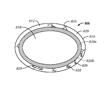
[0016] Fig. 8 is a bottom view of a coated substrate in accordance with
an exemplary
embodiment of the present invention.
DETAILED DESCRIPTION OF THE INVENTION
[0017] One or both surfaces of an optically transparent substrate such as
a lens, a goggle, or a
visor may be coated for a variety of reasons, including to prevent substrate
damage, to reduce glare
and to provide optical filtering. However, most coatings applied to optically
transparent substrates
degrade over time. A variety of mechanisms may account for the degradation
process, including
degradation initiated by delamination of the coating from the substrate.
Polymeric materials have a
low melting point as compared to inorganic materials such as glass or silica.
Depositing coatings
onto polymeric substrates is generally performed at temperatures lower than
the melting points of
the substrates. This may cause the deposited coating to adhere poorly to the
surface of the
substrates. Consequently, the deposited coating may easily delaminate from the
substrate surface
when subjected to a sufficient physical and/or thermal stress.
[0018] Also, optically transparent polymer substrates tend to have
coefficients of thermal
expansion that are sometimes significantly different (e.g., an order of
magnitude higher) than the
coefficients of thermal expansion of the coating materials. Consequently,
optically transparent
polymer substrates tend to expand and contract in response to changes in
temperature at different
rates than the deposited coating materials. The difference between thermal
expansions and
contractions of the coating materials and the substrates means that the
coating materials are
subjected to high physical stress both at lower and higher temperatures than
those used during the
coating deposition. Repeated thermal cycling between high and low temperatures
only exacerbates
the physical stress to which the coating materials are subjected. As a result,
the coating may
delaminate from the substrate forming cracks in the coating and over time
these cracks extend into
the coating materials causing the coating to flake from the surfaces of the
substrate (see Fig. 1).
Delamination may interfere with a user's view through the coated article and
substantial
delamination of a coating from a coated lens substrate may result in total
failure of a coated article,
rendering it useless for its intended purpose.
[0019] Referring to Figs. 1 and 2, there is shown a typical coated
optical device 100 comprising
a substrate 110 having a bottom surface coated with a coating 112. Coating 112
may degrade over
time by delaminating from substrate 110 and developing cracks 104 that
eventually extend into and
obstruct a viewing area 118 (e.g., within boundary line 106) that a user of
the coated article 100
looks through to view objects on the other side of coated optical device 100.
Shaded regions 108
CA 02904605 2015-09-08
WO 2014/159421 PCT/US2014/023572
4
represent portions of coating 112 that have completely delaminated and lifted
off from substrate
110. As shown, a crack 104 in the coating 112 starting at the periphery of
coating 112 can spread
into multiple cracks that progressively advance until eventually extending
past boundary line 106
and into the viewing area 118.
[0020] Referring to Figs. 3-8, the present invention, in exemplary
embodiments, relates to an
optical device, generally designated 300, 600, 700 and 800, and methods of
processing optical
devices that enhance the adhesion between the substrate and the coating and
increases the durability
of the coating (e.g., minimizes or eliminates delamination of the coating from
the substrate).
100211 The optical device of the present invention includes a coated
substrate. The substrate
includes a textured surface portion that increases adhesion of the coating to
the substrate. The
textured surface may increase the surface area in contact with the coating and
achieve a "Velcro-
like" effect between the coating and the substrate. In some embodiments,
treating only an outer
edge area of substrate increases the adhesion between the substrate and the
coating while not
impacting the optical clarity of the area of vision of the optical device.
[0022] Referring to Figs. 3 and 4, a first exemplary embodiment of the
present invention is
shown. Optical device 300 includes a substrate 310 with a coating 312.
Substrate 310 includes a
first surface 314, a peripheral edge 316, an area of vision 318 and a boundary
portion 320 on a
portion of surface 314 extending between peripheral edge 316 and the area of
vision 318. At least a
portion of boundary portion 320 is textured and the coating 312 is applied to
surface 314 over the
area of vision 318 and the textured boundary portion 320.
[0023] Substrate 310 may have any desirable shape, size and thickness.
Substrate 310 may be
shaped for use in or as spectacles, shields, lenses, goggles, visors, windows,
and/or optical sensor
covers. Substrate 310 may have one or more convex and/or concave side
surfaces. In other
embodiments, substrate 310 has one or more flat side surfaces. Substrate 310
may have an optical
power. In other embodiments, substrate 310 has zero optical power. Peripheral
edge 316 may be
generally circular in shape. In other embodiments, peripheral edge 316 is
generally square, oval or a
specific shape such as for a lens or a visor.
[0024] In some embodiments, substrate 310 is comprised of a polymer. In
one embodiment,
substrate 310 is comprised of a thermoset material. In one embodiment, the
thermoset material is
selected from the group consisting of diethylene glycol bis (ally' carbonate)
and diallyl diglycol
carbonate and a combination thereof. In one embodiment, the thermoset material
is selected from
the group consisting of polymers of 1,3 butylene glycol dimethacrilate,
acrylonitrile, allyl
methacrylate, ethoxymethyl methacrylate, ethylene glycol dimethacrylate,
polyethylene glycol
CA 02904605 2015-09-08
WO 2014/159421 PCT/US2014/023572
dimethacrylate, ally! esters, co-polymers of allyl esters with styrene or
vinyl type monomers and
combinations thereof. In some embodiments, substrate 310 comprises a
thermoplastic material. In
one embodiment, the thermoplastic material is selected from the group
consisting of polysulfones,
polyethersulfones, polyamides, polystyrenes, mixtures of polycarbonate and
polyurethanes,
5 polystyrenes, polysulfones, polyesters, acrylics and combinations
thereof. In some embodiments,
substrate 310 comprises a refractive index material. In one embodiment, the
high refractive index
material is selected from the group consisting of high refractive index
copolymers of isocyanates,
urethanes, sulfur-containing aromatic vinyl compounds, and bromine-containing
aromatic acrylic
compounds and combinations thereof.
100251 In one embodiment, coating 312 is a dielectric coating. Dielectric
coatings are
comprised of transparent dielectric materials and may be used for laser
mirrors and/or anti-
reflection. Dielectric coatings, also called thin-film coatings or
interference coatings, may include
thin (e.g., sub-micron) layers of transparent dielectric materials, which are
deposited on substrate
310. Coating 312 may essentially modify the reflective properties of substrate
310 by exploiting the
interference of reflections from multiple optical interfaces. Coating 312 may
be used for highly
reflecting laser mirrors (e.g., to protect a user from damage to their eyes
from lasers) or partially
transmissive output couplers, for dichroic mirrors (treating different
wavelengths differently), for
anti-reflection coatings, for various kinds of optical filters (e.g., for
attenuation of certain
wavelength regions), and thin-film polarizers. Coating 312 may include two or
more (e.g., over a
hundred) of thin-film layers. Coating 312 may include discrete layers (e.g.,
first layer 312a and
second layer 312b shown in Fig. 5) with different refractive indices than one
another. In other
embodiments, coating 312 may include a gradient-index coating, such as a
rugate filter, where the
refractive index is varied continuously through a layer. In one embodiment,
coating 312 includes at
least one metal layer.
[0026] In one embodiment, the melting point of coating 312 is different
from the melting point
of the substrate 310. In one embodiment, coating 312 has a coefficient of
thermal expansion that is
different from the coefficient of thermal expansion of substrate 310. In one
embodiment, coating
312 is comprised of glass. In other embodiments, coating 312 is comprised of
metal, semi-
conductor and/or polymeric material. In one embodiment, coating 312 includes
one or more layers
of Ti02, Si02, A1203, Ta205, MgF2, LaF3 and/or A1F3. In one embodiment,
coating 312 has one or
more layers having a refractive index of approximately 1.3 to approximately
3Ø Coating 312 may
be comprised of any preferred material or combination of materials.
CA 02904605 2015-09-08
WO 2014/159421 PCT/US2014/023572
6
[0027] One or both side surfaces 314, 322 of substrate 310 may include a
coating 312. In one
embodiment, only a portion of a side surface 314, 322 is coated by coating
312. In one
embodiment, coating 312 is on surface 314 intended to face a user's eye or
sensor. In other
embodiments, coating 312 is alternatively, or in addition to, on surface 322
intended to face away
from the user's eye or sensor. In some embodiments, coating 312 includes a
plurality of layers. In
one embodiment, at least one layer of the plurality of coating 312 layers has
the same composition
as at least one other coating layer. In some embodiments, at least one layer
of the coating 312 has a
different composition than at least one other layer of coating 312. In some
embodiments, coating
312 has a thickness in a range of about 1 [im to about 100 pm.
100281 Referring to Figs. 3-5, at least a portion of boundary portion 320,
on surface 314 between
substrate 310 and coating 312 is textured or roughened. Textured boundary
portion 320 is around or
outside the area of vision 318 (e.g., the portion of optical device 300 that
the user looks through). In
one embodiment, textured boundary portion 320 circumscribes or surrounds the
area of vision 318.
In one embodiment, textured boundary portion 320 extends entirely around the
periphery of the area
of vision 318. In one embodiment, textured boundary portion 320 extends from
peripheral edge 316
to the area of vision 318. In one embodiment, the entire boundary portion 320
is textured. In other
embodiments, only a portion of boundary portion 320 is textured. In one
embodiment, a width w,
the distance from the outer edge of textured boundary portion 320 to the inner
edge of textured
boundary portion 320 varies around the area of vision 318. In one embodiment,
width w of
boundary portion 320 is generally constant around the area of vision 318. In
one embodiment,
width w of boundary portion 320 is wider in certain areas (e.g., outside the
view of a user such as
where a strap attaches to a lens) and narrower in other areas (e.g., inside
the view of a user such as a
bottom unsupported edge of a lens or visor). In one embodiment, width w of
boundary portion 320
is approximately 1 mm or greater. In one embodiment, textured boundary portion
320 only partially
extends around the area of vision 318. For example, a top edge along area of
vision 318 may be
void of texturing or texturing may be spotted or spaced around area of vision
318. In one
embodiment, textured boundary portion 320 defines the periphery of area of
vision 318. In other
embodiments, textured boundary portion 320 is spaced from the area of vision
318.
[0029] Referring to Fig. 5, in one embodiment, textured boundary portion
320 forms
microstructures. In one embodiment, textured boundary portion 320 has a
greater surface area than
boundary portion 320 before it was textured. In one embodiment, depth or
thickness t of textured
boundary portion is approximately 1 [im to approximately 100 [im. In one
embodiment, thickness t
of textured boundary portion 320 is approximately 3 [im to approximately 5
[im. In one
CA 02904605 2015-09-08
WO 2014/159421 PCT/US2014/023572
7
embodiment, thickness t of textured boundary portion 320 is variable to form
jagged peaks and
valleys.
[0030] In one embodiment, textured boundary portion 320 is generally
optically opaque. In one
embodiment, opposing surfaces of the substrate 314, 322 within the area of
vision 318 are smooth or
not textured. In other embodiments, surfaces 314, 322 within the area of
vision 318 are textured to a
lesser extent than textured boundary portion 320 such that the area of vision
318 remains optically
transparent. In one embodiment, textured boundary portion 320 is "frosted" as
compared to the area
of vision 318. In one embodiment, textured boundary portion 320 is textured
such that the intensity
of a laser beam going through textured boundary portion 320 is less than 5%
its original intensity.
In one embodiment, textured boundary portion 320 is textured such that the
intensity of a laser beam
going through textured boundary portion 320 is less than 4% its original
intensity. In one
embodiment, textured boundary portion 320 is textured such that the intensity
of a laser beam going
through textured boundary portion 320 is less than 3% its original intensity.
In one embodiment,
textured boundary portion 320 is textured such that the intensity of a laser
beam going through
textured boundary portion 320 is less than 2% its original intensity. In one
embodiment, textured
boundary portion 320 is textured such that the intensity of a laser beam going
through textured
boundary portion 320 is less than 1% its original intensity.
100311 Referring to Fig. 6, there is shown a second exemplary embodiment
of optical device
600. Optical device 600 may include a substrate 610 having a first coating
612b on a first side
surface 614 and a second coating 612a on a second side surface 622. Substrate
may include a
textured boundary portion 620a, 620b on both side surfaces 614, 622 to improve
adhesion of
coatings 612a, 612b. Textured boundary portions 620a, 620b may be the same
size or different
sizes. In one embodiment, coatings 612a, 612b may have the same or different
optical properties
than one another. In one embodiment, an additional substrate 624 may be
included to sandwich
coating 612b between substrates 610, 624. Including an additional substrate
624 may provide
protection to a user's eyes should optical device 600 be damages causing
coating 612b to detach
and/or to provide an optical function such as filtering. Additional layers of
substrates and coatings
may be provided.
[0032] Referring to Fig. 7, in a third exemplary embodiment, optical
device 700 includes an
initial peripheral edge of 716a that is trimmed (e.g., cut or ground) to a
reduced final peripheral edge
716b. In one embodiment, boundary portion 720 is textured to the initial
peripheral edge and the
final width of the textured boundary portion 720 is determined by the trimming
of initial peripheral
edge 716a down to the final peripheral edge 716b. Trimming the textured
boundary portion 720
CA 02904605 2015-09-08
WO 2014/159421 PCT/US2014/023572
8
may assist in processing (e.g., holding a rounded shape during texturing and
coating) particularly if
the final peripheral edge 716b has a non-circular shape and/or the width of
the remaining textured
boundary portion 720 is small.
[0033] Referring to Fig. 8, there is shown a fourth exemplary embodiment
of optical device 800.
Optical device 800 may include a boundary portion 820 that is only partially
textured (shaded area).
Textured boundary portion 820a extends from the area of vision 818 to a
textured boundary 820b
spaced inwardly from peripheral edge 816. The textured boundary 820b may be a
sharply defined
line as shown. In other embodiments, the textured boundary 820b is faded such
that the amount of
texturing decreases toward the peripheral edge 816. In one embodiment, any
delamination such as
cracks 826 or chips 828 formed between coating 812 and the substrate are
stopped at textured
boundary 820b and are prevented from extending to the area of vision 820.
[0034] Referring to Figs. 3-5, the texturing of boundary portion 320 may
be any preferred
method. In one embodiment, area of vision 318 is covered or otherwise
protected before texturing
boundary portion 320. In one embodiment, texturing of boundary portion 320 is
a mechanical
process. In one embodiment, the texturing step is performed by abrasive
blasting the boundary
portion 320. The abrasive blasting is conducted by forcibly propelling a
stream of abrasive material
against surface 314 under high pressure to roughen boundary portion 320. The
abrasive blasting
may include the use of a soft abrasive material. In one embodiment, the soft
abrasive material
comprises particles of sodium bicarbonate. In one embodiment, the particles of
sodium bicarbonate
have an average size of about 50 micron. In one embodiment, the soft abrasive
material comprises
particles of dry ice. In one embodiment, the soft abrasive material comprises
particles of
magnesium sulfate. Other mechanical processes may be used for texturing such
as scrapping or
ultrasonic roughening.
[0035] In one embodiment, texturing of boundary portion 320 is a chemical
texturing process.
Chemical texturing may refer to using an acid solution, alkaline solution,
oxidizing agent, reducing
agent or any other solution to etch microstructures into substrate 310.
[0036] In one embodiment, texturing of boundary portion 320 is an optical
texturing process. In
one embodiment, texturing of boundary portion 320 is performed with a laser
light beam having a
wavelength of about 1.064 [tm. Any laser may be utilized having any desired
wavelength.
[0037] In one embodiment, texturing of boundary portion 320 is achieved by
the configuration
of the substrate mold. For examples, a surface of the mold used to form
substrate 310 may be
textured such that surface 314 contacting the roughened mold feature results
in the textured
boundary portion 320.
CA 02904605 2015-09-08
WO 2014/159421 PCT/US2014/023572
9
[0038] In other embodiments, texturing of boundary portion 320 is a
combination of any of the
processes described above.
[0039] Once surface 314 of substrate 310 has been sufficiently textured,
coating 312 is applied
to surface 314. Coating 312 may be deposited to substrate 310 in any preferred
manner. In one
embodiment, coating 312 is applied to substrate 310 by a vacuum vapor
deposition process. In one
embodiment, coating 312 is deposited on a spinning substrate 310 to spread
coating 312 over
surface 314. In one embodiment, coating 312 is sprayed onto substrate 310. In
one embodiment,
coating 312 is electron beam deposited onto substrate 310. In one embodiment,
coating 312 is ion-
assisted deposited (TAD) onto substrate 310. In one embodiment, coating 312 is
ion beam sputtered
(IBS) onto substrate 310. In one embodiment, coating is advanced plasma
reactive sputtered
(APRS) onto substrate 310.
[0040] In one embodiment, a thermally curable coating composition 312
is applied to substrate
310. In one embodiment, a radiation curable coating composition 312 is applied
substrate 310. In
one embodiment, ultra violet (UV) curable coating composition 312 is applied
to substrate 310 and
then irradiated with UV radiation to form coating 312.
[0041] In some embodiments, coating 312 becomes integral with substrate
310. In one
embodiment, substrate 310 is considered to be "grown" or thickened with the
additional material of
coating 312. In one embodiment, coating 312 flows into and bonds with the
microstructures of the
textured boundary portion 320.
[0042] In some embodiments, after depositing coating 312 onto substrate 310
an additional
substrate layer 624 (see Fig. 6) may be attached to coating 312. In some
embodiments, after
depositing coating 312 onto substrate 310 the optical device 300 is trimmed
down to reduce the
width w of boundary portion 320 (see Fig. 7).
[0043] In one embodiment, the method making optical device 300 results in
an adhesion
between substrate 310 and coating 312 that is substantially improved compared
with coated
substrates whose surfaces have not been roughened. In one embodiment, enhanced
adhesion
between substrate 310 and coating 312 prevents coating 312 from delaminating
or prevent any
delamination from propagating into the area of vision 318.
[0044] It will be appreciated by those skilled in the art that changes
could be made to the
exemplary embodiments shown and described above without departing from the
broad inventive
concept thereof. It is understood, therefore, that this invention is not
limited to the exemplary
embodiments shown and described, but it is intended to cover modifications
within the spirit and
scope of the present invention as defined by the claims. For example, specific
features of the
CA 02904605 2015-09-08
WO 2014/159421 PCT/US2014/023572
exemplary embodiments may or may not be part of the claimed invention and
features of the
disclosed embodiments may be combined. The words "top" and "bottom" designate
directions in
the drawings to which reference is made. Unless specifically set forth herein,
the terms "a", "an"
and "the" are not limited to one element but instead should be read as meaning
"at least one".
5 [0045] It is to be understood that at least some of the figures and
descriptions of the invention
have been simplified to focus on elements that are relevant for a clear
understanding of the
invention, while eliminating, for purposes of clarity, other elements that
those of ordinary skill in the
art will appreciate may also comprise a portion of the invention. However,
because such elements
are well known in the art, and because they do not necessarily facilitate a
better understanding of the
10 invention, a description of such elements is not provided herein.
[0046] Further, to the extent that the method does not rely on the
particular order of steps set
forth herein, the particular order of the steps should not be construed as
limitation on the claims.
The claims directed to the method of the present invention should not be
limited to the performance
of their steps in the order written, and one skilled in the art can readily
appreciate that the steps may
be varied and still remain within the spirit and scope of the present
invention.