Note: Descriptions are shown in the official language in which they were submitted.
81791467
- 1 -
COMPLEMENTARY METAL OXIDE SEMICONDUCTOR (CMOS) ULTRASONIC
TRANSDUCERS AND METHODS FOR FORMING THE SAME
[0001]
BACKGROUND
Field
[0002] The technology described herein relates to complementary metal
oxide
semiconductor (CMOS) transducers and methods for forming the same.
Related Art
[0003] Capacitive Micromachined Ultrasonic Transducers (CMUTs) are known
devices that include a membrane above a micromachined cavity. The membrane may
be used
to transduce an acoustic signal into an electric signal, or vice versa. Thus,
CMUTs can
operate as ultrasonic transducers.
[0004] Two types of processes can be used to fabricate CMUTs.
Sacrificial layer
processes form the membrane of the CMUT on a first substrate above a
sacrificial layer.
Removal of the sacrificial layer leaves behind the membrane above a cavity.
Wafer bonding
processes bond two wafers together to form a cavity with a membrane.
SUMMARY
[0005] According to an aspect of the technology, an apparatus is
provided comprising
an ultrasonic transducer and an integrated circuit coupled to the ultrasonic
transducer, the
integrated circuit formed in a CMOS wafer. In at least some embodiments, such
a
configuration allows for a compact, fully integrated ultrasound device to be
made. The
CA 2905040 2020-03-19
CA 02905040 2015-09-09
WO 2014/151525 PCT/1JS2014/025924
-2-
ultrasonic transducer comprises a cavity formed in the CMOS wafer, a membrane
formed of a
material other than monocrystalline silicon overlying the cavity, and an
electrical contact
providing electrical connectivity between the membrane and the integrated
circuit. In at least
some embodiments, the use of a material other than monocrystalline silicon as
the membrane
facilitates fabrication of the device by not involving a monocrystalline
material. In at least
some embodiments, the use of monocrystalline materials requires more
fabrication effort and
time to be expended compared to use of materials which are not
monocrystalline.
[0006] According to an aspect of the technology, a method of forming an
ultrasonic
transducer is provided, comprising forming a cavity in a CMOS wafer, and
bonding a transfer
wafer to the CMOS wafer, the transfer wafer having a front face formed of a
material not
including monocrystalline silicon. The front face may be the face of the
transfer wafer
arranged to contact the CMOS wafer. In some embodiments, the transfer wafer
may include
one or more handle layers, and the front face may be opposite the handle
layer(s). Bonding
the transfer wafer to the CMOS wafer is, in some embodiments, performed below
450 C,
which facilitates fabrication of the ultrasonic transducer without damaging
integrated circuitry
and/or metal layers having been formed on the CMOS wafer prior to bonding. As
described
previously, using a material other than monocrystalline silicon for the
transfer wafer may
facilitate fabrication by requiring less effort and time to be expended
compared to if a
monocrystalline material was used.
[0007] According to an aspect of the technology, an apparatus is provided,
comprising
a complementary metal oxide semiconductor (CMOS) wafer having an integrated
circuit (IC)
formed therein, a membrane disposed above a cavity in the CMOS wafer, the
membrane being
integrated with the CMOS wafer and having a first side proximate the cavity
and a second
side distal the cavity, and a conductive electrical path contacting the first
side of the
membrane proximate the cavity and electrically connecting the membrane to the
IC. In some
embodiments, such a configuration is the basis of, or represents, a device
including an
integrated ultrasonic transducer and integrated circuit. Thus, a compact
ultrasound device
may be made by allowing formation of the device components on a single CMOS
wafer.
[0008] In at least some embodiments, the provision for a conductive
electrical path
contacting the first side of the membrane proximate the cavity and
electrically connecting the
CA 02905040 2015-09-09
WO 2014/151525 PCT/1JS2014/025924
-3-
membrane to the IC facilitates integration of an ultrasonic transducer and the
IC by obviating
the need to have an electrical contact on a side of the membrane facing away
from the cavity.
[0009] In some embodiments, the cavity is defined at least in part by a
conductive
sidewall formed of a conductive material and the conductive electrical path
comprises at least
a portion of the conductive sidewall. In some such embodiments, formation of
the conductive
electrical path is facilitated by utilizing the sidewall which defines a
boundary of the cavity.
In some embodiments, the conductive sidewall comprises a metal and the first
side of the
membrane comprises a layer of the metal, which configuration facilitates
integration of the
membrane with the conductive sidewall in at least some embodiments, for
example by
bonding. In some embodiments, titanium nitride (TiN) is used for the
conductive sidewall
and/or the layer on the first side of the membrane. In some embodiments, the
cavity is defined
at least in part by a non-conductive sidewall and the conductive electrical
path comprises an
embedded via in the non-conductive sidewall. Such a configuration provides
beneficial
electrical insulating properties by not leaving the conductive electrical path
exposed as a
boundary of the cavity.
[0010] In some embodiments, the membrane comprises polysilicon, and in
some
embodiments amorphous silicon. The use of such materials may relax fabrication
by avoiding
the use of monocrystalline materials. As previously described, the use of such
materials
requires less effort and time than fabrication with monocrystalline materials,
in at least some
embodiments. In some embodiments, the membrane comprises degeneratively doped
silicon,
which in some embodiments contributes to the membrane being electrically
conductive.
[0011] In some embodiments, the membrane has a non-uniform thickness
including a
center portion having a first thickness and an outer portion having a second
thickness. In
some embodiments, the second thickness is less than the first thickness, such
that the
membrane may be configured as a piston. In some embodiments, the first
thickness is less
than the second thickness. In some embodiments, the second thickness is
between
approximately one micron and approximately five microns, and in some
embodiments is
between approximately 0.1 microns and approximately two microns. In some
embodiments,
the first thickness is between approximately one micron and approximately 50
microns.
CA 02905040 2015-09-09
WO 2014/151525 PCT/1JS2014/025924
-4-
[0012] The provision for membranes with non-uniform thicknesses
facilitates
achieving desired operation of the membrane, such as desired frequency and/or
power
characteristics.
[0013] In some embodiments, the CMOS wafer includes a plurality of
cavities and a
plurality of membranes above respective cavities of the plurality of cavities
defining a
plurality of ultrasonic transducers. In some embodiments, the membranes are
arranged to seal
the respective cavities. In some embodiments, the plurality of ultrasonic
transducers are
configured as at least part of an ultrasound imaging device, which may
function to collect
ultrasound data suitable for forming ultrasound images. In some embodiments,
the plurality
of ultrasonic transducers are configured as at least part of a high intensity
focused ultrasound
(HIFU) device, which may function to apply HIFU energy to a target subject. In
some
embodiments, the plurality of ultrasonic transducers are configured to form a
device operable
as an ultrasound imaging device and/or a high intensity focused ultrasound
(HIFU) device,
and in some embodiments are configured to form a device operable as an imaging
device and
a HIFU device to perform image-guided HIFU, for example in which ultrasound
data
collected by at least some of the ultrasonic transducers is used to form an
ultrasound image
which may be considered in applying HIFU to a subject.
[0014] In some embodiments, the apparatus further comprises an electrode
in the
CMOS wafer beneath the cavity, for example being positioned proximate an end
of the cavity
opposite an end at which the membrane(s) is located. In some embodiments, the
cavity has a
first width and the electrode has a second width. In some embodiments, the
first width is
greater than the second width, which may allow for an ultrasonic transducer
comprising the
cavity to exhibit beneficial capacitive characteristics. In some embodiments,
the first width is
approximately equal to the second width, and in some embodiments the first
width is less than
the second width, which in some embodiments minimizes undesirable capacitive
behavior by
increasing a distance between the electrode and sidewalls of the cavity. In
some
embodiments, the electrode comprises TiN.
[0015] According to an aspect of the technology, an ultrasonic transducer
is provided,
comprising a substrate having a cavity formed therein, and a membrane
integrated with the
substrate and overlying the cavity. In some embodiments, the membrane is
configured to seal
the cavity. In some embodiments, the membrane has a thickness between
approximately 0.05
CA 02905040 2015-09-09
WO 2014/151525 PCT/1JS2014/025924
-5-
microns and approximately 1 micron, which facilitates beneficial operation of
the ultrasonic
transducer, for example with respect to a desired frequency or range of
frequencies.
[0016] In some embodiments, the substrate is a complementary metal oxide
semiconductor (CMOS) wafer having an integrated circuit (IC) formed therein
and the
membrane is monolithically integrated with the substrate. In at least some
embodiments, such
a configuration allows for a compact ultrasonic transducing device to be made
by allowing the
components to be integrated with the same substrate.
[0017] In some embodiments, the membrane has a thickness between
approximately
0.1 microns and approximately 0.5 microns. In some embodiments, the membrane
comprises
polysilicon, and in some embodiments the membrane comprises amorphous silicon.
The use
of such materials requires less effort and time than fabrication with
monocrystalline materials,
in at least some embodiments.
[0018] In some embodiments, the membrane has a non-uniform thickness,
including a
center portion having a first thickness and an outer portion having a second
thickness. In
some embodiments. the first thickness is less than the second thickness. In
some
embodiments, the second thickness is less than the first thickness, such that
the membrane
may be configured as a piston. In some embodiments, the second thickness is
between
approximately one micron and approximately five microns, and in some
embodiments is
between approximately 0.1 microns and approximately two microns. In some
embodiments,
the first thickness is between approximately one micron and approximately 50
microns. In
some embodiments, the center portion is configured as a mass for the membrane,
for example
having a greater thickness than a thickness of the periphery of the membrane.
The provision
for membranes with non-uniform thicknesses facilitates achieving desired
operation of the
membrane, such as desired frequency and/or power characteristics.
[0019] According to an aspect of the technology, a method is provided
comprising
forming an ultrasonic transducer by forming a conductive electrical path
connecting an
integrated circuit (IC) in a complementary metal oxide semiconductor (CMOS)
wafer to a first
side of a membrane covering a cavity in the CMOS wafer, the first side of the
membrane
being proximate the cavity and the membrane further having a second side
distal the cavity.
The provision for a conductive electrical path as described may facilitate
integration of an
CA 02905040 2015-09-09
WO 2014/151525 PCT/1JS2014/025924
-6-
ultrasonic transducer and the IC by obviating the need to have an electrical
contact on a side
of the membrane facing away from the cavity.
[0020] In some embodiments, forming the conductive electrical path
connecting the IC
in the CMOS wafer to the first side of the membrane comprises forming the
conductive
electrical path in the CMOS wafer and subsequently monolithically integrating
the membrane
with the CMOS wafer. Thus, in some embodiments the electrical connection to
the membrane
may be completed when the membrane is integrated with the CMOS wafer.
[0021] In some embodiments, monolithically integrating the membrane with
the
CMOS wafer comprises performing a wafer bonding process to bond a transfer
wafer with the
CMOS wafer. The wafer bonding process is performed below 450 C, which may
provide the
benefit previously described in term of not damaging integrated circuitry
and/or metal layers.
In some embodiments, the method further comprises forming the membrane from
the transfer
wafer subsequent to bonding the transfer wafer with the CMOS wafer. In at
least some
embodiments, forming the membrane from a transfer wafer after bonding allows
for use of a
thicker transfer wafer which facilitates wafer bonding.
[0022] In some embodiments, the membrane has a non-uniform thickness
including a
center portion having a first thickness and an outer portion having a second
thickness less than
the first thickness and monolithically integrating the membrane with the CMOS
wafer
comprises forming a seal between the outer portion of the membrane and a
topside of a
sidewall of the cavity. The topside of the sidewall of the cavity may be an
exposed side of the
sidewall and in some embodiments may define at least in part a depth of the
cavity. In some
embodiments, the topside may represent a bonding surface.
[0023] In some embodiments, the method further comprises forming the
cavity in the
CMOS wafer at least in part by forming a conductive sidewall of the cavity. In
some
embodiments, the conductive electrical path comprises at least a portion of
the conductive
sidewall. In some such embodiments, formation of the conductive electrical
path is facilitated
by utilizing the sidewall which defines a boundary of the cavity. In some
embodiments, the
conductive sidewall comprises a metal, and the first side of the membrane
comprises a layer
of the metal, which configuration facilitates integration of the membrane with
the conductive
sidewall in at least some embodiments, for example by bonding. In some
embodiments, the
conductive sidewall and/or layer of the membrane comprises titanium nitride
(TiN).
CA 02905040 2015-09-09
WO 2014/151525 PCT/1JS2014/025924
-7-
[0024] In some embodiments, the method further comprises forming the
cavity in the
CMOS wafer at least in part by forming a non-conductive sidewall of the
cavity. In some
embodiments, forming the conductive electrical path comprises forming an
embedded via in
the non-conductive sidewall of the cavity. In some embodiments, such a
configuration
provides beneficial electrical insulating properties by not leaving the
conductive electrical
path exposed as a boundary of the cavity. In some embodiments, the method
further
comprises forming the membrane of polysilicon, and in some embodiments further
comprises
forming the membrane of amorphous silicon, which in at least some embodiments
involves
less fabrication effort and time than does using monocrystalline materials.
[0025] In some embodiments, the membrane has a non-uniform thickness
including a
center portion having a first thickness and an outer portion having a second
thickness less than
the first thickness. In some embodiments, the second thickness is between
approximately one
micron and approximately five microns, and in some embodiments the second
thickness is
between approximately 0.1 microns and approximately two microns. In some
embodiments,
the first thickness is between approximately one micron and approximately 50
microns. In
some embodiments, the membrane is configured as a piston. The provision for
membranes
with non-uniform thicknesses facilitates achieving desired operation of the
membrane, such as
desired frequency and/or power characteristics.
[0026] According to an aspect of the technology, a method of making an
ultrasonic
transducer is provided, comprising forming a covered cavity in a complementary
metal oxide
semiconductor (CMOS) wafer by sealing the cavity with a polysilicon or
amorphous silicon
membrane. In at least some embodiments, such a configuration allows for
fabrication of an
ultrasonic transducer with less fabrication effort and time than would be
involved in using a
monocrystalline material.
[0027] In some embodiments, forming the sealed cavity comprises forming
the cavity
in the CMOS wafer, bonding the CMOS wafer with a transfer wafer comprising a
layer of
polysilicon or amorphous silicon, and forming the membrane from the layer of
polysilicon or
amorphous silicon of the transfer wafer. In some embodiments, bonding the CMOS
wafer
with the transfer wafer comprises performing the bonding below 450 C, which
may provide
the benefit previously described in terms of not damaging integrated circuitry
and/or metal
layers. In some embodiments, forming the membrane from the layer of
polysilicon or
CA 02905040 2015-09-09
WO 2014/151525 PCT/1JS2014/025924
-8-
amorphous silicon of the transfer wafer comprises thinning the layer of
polysilicon or
amorphous silicon, which technique in some embodiments allows for use of
thicker transfer
wafers for wafer bonding. In some embodiments, the transfer wafer is a multi-
layer wafer
including a base silicon layer, an insulating layer, and the layer of
polysilicon or amorphous
silicon. In some embodiments, the layer of polysilicon or amorphous silicon is
a layer of
polysilicon, and in some embodiments is a layer of amorphous silicon, which
embodiments
may facilitate fabrication by involving less fabrication effort and time than
would be involved
in using monocrystalline materials. In some embodiments, forming the membrane
from the
layer of polysilicon or amorphous silicon of the transfer wafer comprises
removing the base
silicon layer and the insulating layer.
[0028] In some embodiments, forming the sealed cavity in the CMOS wafer
comprises
sealing the cavity with a polysilicon membrane, and in some embodiments
comprises sealing
the cavity with an amorphous silicon membrane. In at least some embodiments,
such a
technique allows for fabrication of an ultrasonic transducer with less
fabrication effort and
time than would be involved in using a monocrystalline material.
[0029] In some embodiments, the membrane has a non-uniform thickness
including a
center portion having a first thickness and an outer portion having a second
thickness less than
the first thickness. In some embodiments, an outer portion of the membrane has
a first
thickness and the method further comprises forming a center portion of the
membrane having
a second thickness greater than the first thickness subsequent to sealing the
cavity with the
polysilicon or amorphous silicon membrane. In some embodiments, forming the
center
portion of the membrane having the second thickness comprises depositing and
patterning a
first material on the membrane. In some embodiments, depositing and patterning
the first
material is performed below 450 C, which may provide the benefit previously
described in
terms of not damaging integrated circuitry and/or metal layers. In some
embodiments, the
first material is not polysilicon or amorphous silicon. In some embodiments,
the polysilicon
or amorphous silicon membrane is degeneratively doped, which in at least some
embodiments
facilitates making electrical contact to the membrane.
[0030] In all such embodiments in which a membrane is disposed above a
cavity, the
membrane may optionally be configured to seal the cavity.
CA 02905040 2015-09-09
WO 2014/151525 PCT/1JS2014/025924
-9-
BRIEF DESCRIPTION OF THE DRAWINGS
[0031] Various aspects and embodiments of the application will be
described with
reference to the following figures. It should be appreciated that the figures
are not necessarily
drawn to scale. Items appearing in multiple figures are indicated by the same
reference
number in all the figures in which they appear.
[0032] FIGs. IA-1K illustrate a process sequence for fabricating a CMOS
ultrasonic
transducer (CUT) having a membrane formed above a cavity in a CMOS wafer,
according to a
non-limiting embodiment of the present application.
[0033] FIGs. 2A-2C illustrate a process sequence for fabricating a CUT
having a
piston membrane in which the piston membrane is transferred from a transfer
wafer,
according to a non-limiting embodiment of the present application.
[0034] FIGs. 3A-3B illustrate a process sequence for forming an
alternative CUT
having a piston membrane, in which the piston membrane is formed after wafer
bonding,
according to a non-limiting embodiment of the present application.
[0035] FIGs. 4A-4C illustrate an alternative process sequence for forming
a CUT
having a piston membrane, in which the piston membrane is transferred from a
transfer wafer,
according to a non-limiting embodiment of the present application.
[0036] FIG. 5 illustrates a CUT having a membrane stop disposed on a
bottom surface
of a cavity of the CUT, according to a non-limiting embodiment of the present
application.
[0037] FIG. 6 illustrates a CUT having a piston membrane and a membrane
stop
disposed on a bottom portion of the cavity of the CUT, according to a non-
limiting
embodiment of the present application.
[0038] FIGs. 7A-7H illustrate a process sequence for forming a CUT having
a via
embedded in a CMOS wafer to make electrical contact to a bottom side of a
membrane of the
CUT, according to a non-limiting embodiment of the present application.
[0039] FIGs. 8A-8B illustrate a process sequence for forming a piston
membrane from
the device resulting from the process of FIGs. 7A-7H, according to a non-
limiting
embodiment of the present application.
CA 02905040 2015-09-09
WO 2014/151525 PCT/1JS2014/025924
-10-
[0040] FIGs. 9A-9B illustrate a process sequence for forming a CUT having
a piston
membrane transferred from a transfer wafer and having an embedded via in a
CMOS wafer to
make electrical contact to the bottom side of the membrane, according to a non-
limiting
embodiment of the present application.
[0041] FIGs. 10A-10H illustrate a process sequence for forming a CUT
having a
piston membrane and an embedded via through the membrane to make electrical
contact to a
CMOS wafer, according to a non-limiting embodiment of the present application.
[0042] FIG. 11 illustrates an alternative CUT to that resulting from the
process of
FIGs. 10A-10H that includes a piston membrane having a thicker center portion
than that of
the CUT in FIG. 10H.
[0043] FIG. 12 illustrates a CUT having a lined via to make electrical
contact between
a CMOS wafer and a top side of a membrane of the CUT, according to a non-
limiting
embodiment of the present application.
[0044] FIGs. 13A-13I illustrate a process sequence for forming a CUT
having
electrical contacts on a top side of a membrane of the CUT, according to a non-
limiting
embodiment of the present application.
[0045] FIG. 14 illustrates an alternative CUT to that resulting from the
process of
FIGs. 13A-13I that includes an electrode beneath a cavity of the CUT that is
narrower than a
width of the cavity, according to a non-limiting embodiment of the present
application.
[0046] FIG. 15 illustrates an alternative CUT to that of FIG. 14 in which
the CUT
includes a piston membrane, according to a non-limiting embodiment of the
present
application.
[0047] FIGs. 16A-16B illustrate a process sequence for forming an
alternative CUT
having a piston membrane and top side electrical contacts to the membrane,
according to a
non-limiting embodiment of the present application.
[0048] FIGs. 17A-17C illustrate a process sequence for forming a CUT
having a
piston membrane and top side electrical contacts to the membrane, according to
a non-limiting
embodiment of the present application.
CA 02905040 2015-09-09
WO 2014/151525 PCT/1JS2014/025924
-11-
[0049] FIGs. 18A-18E illustrate an alternative process sequence for
forming a CUT
having a piston membrane and top side electrical contacts to the membrane,
according to a
non-limiting embodiment of the present application.
[0050] FIGs. 19A-19B illustrate a further alternative process sequence for
forming a
CUT having a piston membrane and top side electrical contacts to the membrane,
according to
a non-limiting embodiment of the present application.
[0051] FIGs. 20A-20I illustrate a process sequence for forming a CUT
having
electrical contacts on a top side of a membrane of the CUT and having a
membrane stop on a
bottom surface of a cavity of the CUT, according to a non-limiting embodiment
of the present
application.
[0052] FIGs. 21A-21F illustrate a process sequence for forming a CUT
having
electrical contacts on a top side of a membrane of the CUT and having a
membrane stop on a
bottom side of the membrane, according to a non-limiting embodiment of the
present
application.
[0053] FIGs. 22A-22D illustrate various shapes for cavities of CUTS,
according to
non-limiting embodiments of the present application.
[0054] FIGs. 23A-23D illustrate a process sequence for fabricating a
transfer wafer
having a piston formed therein, according to a non-limiting embodiment of the
present
application.
[0055] FIGs. 24A-24B illustrate a process sequence for fabricating a
transfer wafer
having a membrane stop, according to a non-limiting embodiment of the present
application.
[0056] FIGS. 25A-25B illustrate an alternative process sequence for
fabricating a
transfer wafer having a piston formed therein, according to a non-limiting
embodiment of the
present application.
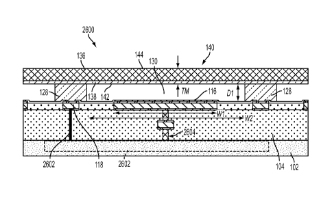
[0057] FIG. 26 illustrates the ultrasonic transducer of FIG. 1K connected
to an
integrated circuit in the CMOS wafer, with the integrated circuit disposed
beneath the
ultrasonic transducer.
CA 02905040 2015-09-09
WO 2014/151525 PCT/1JS2014/025924
-12-
DETAILED DESCRIPTION
[0058] Existing methods for forming CMUTs are impractical for forming
ultrasonic
transducers integrated with CMOS wafers and, therefore, CMOS integrated
circuits (ICs) on
such wafers. Thus, such integrated ultrasonic transducers and ICs are
nonexistent today. For
example, existing methods for forming CMUTs do not provide a practical manner
for making
electrical connection between the CMUT and integrated circuits on a CMOS
wafer. Also,
existing methods do not adequately allow for scaling of CMUTs to sizes
appropriate for
compatibility with low voltage CMOS integrated circuits. Furthermore, CMUT
manufacturing processes are too complex to be performed in a cost-effective
manner suitable
for large scale production of commercial devices, for example because they
involve
processing with complex materials and too many processing steps.
[0059] Accordingly, aspects of the present application provide scalable,
relatively low
cost methods of fabricating ultrasonic transducers integrated with CMOS wafers
and, in some
embodiments, CMOS ICs formed on the CMOS wafers. Such methods enable the
formation
of a new class of devices including monolithically integrated ultrasonic
transducers and
CMOS ICs, referred to herein as CMOS Ultrasonic Transducers (CUTs). The CUTs
may be
used to form ultrasound devices for ultrasound imaging and/or high intensity
focused
ultrasound (HIFU) applications and/or other ultrasound applications.
[0060] To facilitate integration of ultrasonic transducer technology with
CMOS
processing techniques in a manner suitable for scalable, large scale
production of CUTs, it
may be desirable for a manufacturing process to exhibit one or more of various
characteristics.
For example, the process may be suitable for forming ultrasonic transducers
without damaging
the CMOS wafer and any circuitry (e.g., an IC) formed thereon. Thus, the
process may avoid
processing steps which require temperatures sufficiently high to cause damage
to a CMOS
wafer and CMOS ICs. Rather, low temperature processes may be employed. The
process
may utilize materials common to CMOS process lines, and which do not require
extensive
effort or time to fabricate and/or deposit, such as polycrystalline and/or
amorphous forms of
materials rather than single crystal (monocrystalline) forms. The process may
provide for
suitable manners of making direct or indirect electrical connection to
individual ultrasonic
transducer cells. The process may also be suitable for making ultrasonic
transducers of
suitable sizes to enable low voltage operation (e.g., below 70 V, below 50 V,
below 30 V, or
other suitably low voltages for transducer operation), thus making them more
compatible with
CA 02905040 2015-09-09
WO 2014/151525 PCT/1JS2014/025924
-13-
low voltage CMOS ICs. For example, the processes may be suitable for making
membranes
of sufficient sizes (e.g., sufficiently small thicknesses) and shapes for
operation as low voltage
devices while still delivering desired transducer behavior (e.g., desired
frequencies of
operation, bandwidths, power, or other characteristics). Other characteristics
of a
manufacturing process may also be desirable in some embodiments to facilitate
integration of
ultrasonic transducers with CMOS wafers.
[0061] Accordingly, aspects of the present application implement low
temperature
(e.g., below 450 C) wafer bonding to form ultrasonic transducer membranes on
CMOS
wafers. Low temperature in this context may, in some embodiments, be below 450
C, below
400 C, below 350 C, between 200 C and 450 C, any temperature within that
range, or any
suitable temperature for preserving structures on a CMOS wafer). Thus, the
bonding
processes as well as other fabrication steps for forming CUTs according to
some embodiments
may avoid any anneals above 450 C. In some embodiments, the membranes may be
formed
of relatively simple and inexpensive materials, such as polycrystalline
silicon, amorphous
silicon, silicon dioxide, silicon nitride (SiN), and titanium nitride (TiN).
The membranes may
also be thin, and in at least some embodiments thinner than those previously
achievable in
CMUTs. Use of such thin membranes may facilitate the formation of ultrasonic
transducers
operable at voltages sufficiently low to comply with CMOS technology, and thus
may
facilitate formation of CUTs.
[0062] Aspects of the present application provide various designs and
processes for
making electrical connection to the membrane of an ultrasonic transducer in a
manner that
facilitates integration of the ultrasonic transducer with a CMOS integrated
circuit. In some
embodiments, connection may be made from a cavity-side (e.g., a bottom side)
of the
membrane. Such connection may be made by way of an embedded via, a conductive
standoff
or cavity wall, or in any other suitable manner. Such electrical
interconnections may provide
local connection to the membrane rather than global connection, whereby the
connection to
individual membranes may be made close to related circuitry and on an
individual basis rather
than at great distances from related circuitry and on a multi-membrane basis.
Such capability
for local connection to membranes may enable a broader range of operating
schemes than
those afforded by global interconnection, for example because of the
capability for
individualized control of membranes.
CA 02905040 2015-09-09
WO 2014/151525 PCT/1JS2014/025924
-14-
[0063] Aspects of the present application provide CUTs having a piston
configuration,
in which a membrane includes one or more relatively thick center portions and
a relatively
thin surrounding (or outer) portion. Such a structure may be referred to
herein as a piston
membrane. In some embodiments, the piston membrane may be fully formed on a
transfer
wafer prior to wafer bonding. The transfer wafer may then be bonded to a CMOS
wafer with
low temperature processing methods and the piston membrane removed from the
remainder of
the transfer wafer. In this manner. piston membranes formed of a single
material defining a
unitary body may be formed, and such piston membranes may be formed of
materials that are
processed at temperatures sufficiently high to damage CMOS ICs if such
processing had
occurred after the wafer bonding.
[0064] The aspects and embodiments described above, as well as additional
aspects
and embodiments, are described further below. These aspects and/or embodiments
may be
used individually, all together, or in any combination of two or more, as the
application is not
limited in this respect.
[0065] A first process for forming an ultrasonic transducer having a
membrane above
a cavity in a CMOS wafer is now described. Referring to FIG. 1A, the process
may begin
with a CMOS wafer 100 including a substrate 102, a dielectric or insulating
layer 104, a first
metallization layer 106 and a second metallization layer 108, which in some
embodiments
may be a top metallization layer of the CMOS wafer 100.
[0066] The substrate 102 may be silicon or any other suitable CMOS
substrate. In
some embodiments. the CMOS wafer 100 may include CMOS integrated circuitry
(IC), and
thus the substrate 102 may be a suitable substrate for supporting such
circuitry.
[0067] The insulating layer 104 may be formed of SiO2 or any other
suitable dielectric
insulating material. In some embodiments, the insulating layer 104 may be
formed via
tetraethyl orthosilicate (TEOS), though alternative processes may be used.
[0068] While the CMOS wafer 100 is shown as including two metallization
layers 106
and 108, it should be appreciated that CMOS wafers according to the various
aspects of the
present application are not limited to having two metallization layers, but
rather may have any
suitable number of metallization layers, including more than two in some
embodiments. Such
CA 02905040 2015-09-09
WO 2014/151525 PCT/1JS2014/025924
-15-
metallization layers may be used for wiring (e.g., as wiring layers) in some
embodiments,
though not all embodiments are limited in this respect.
[0069] The first and second metallization layers 106 and 108 may have any
suitable
construction. In the embodiment illustrated, at least the second metallization
layer 108 may
have a multi-layer construction, including a middle conductive layer 112
(e.g., formed of
aluminum or other suitable conductive material) and upper and lower liner
layers 110 and 114,
respectively. The liner layers 110 and 114 may be formed of titanium nitride
(TiN) or other
suitable conductive material (e.g., metals other than TiN, such as tantalum,
or other suitable
metals for acting as a liner). In some embodiments, the upper liner layer 110
may be used as
an etch stop, for example during one or more etch steps used in as part of a
process for
forming a cavity for an ultrasonic transducer. Thus, the liner layer 110 may
be formed of a
material suitable to act as an etch stop in some embodiments. Moreover, while
not shown, the
first and second metallization layers 106 and 108, as well as any other
metallization layers
described herein, may optionally include silicon oxynitride (SiON) as an upper
layer (e.g., on
top of liner layer 110) to serve as an anti-reflective coating during
lithography stages.
[0070] In some embodiments, it may be desirable to form an electrode from
the
second metallization layer 108 serving as an electrode of an ultrasonic
transducer. Also, the
second metallization layer 108 may be used to make electrical contact to a
membrane of a
CUT to be formed on the CMOS wafer. Accordingly, as shown in FIG. 1B, the
second
metallization layer 108 may be suitably patterned to form an electrode 116 and
one or more
contacts 118.
[0071] While FIG. 1B illustrates a configuration in which an electrode and
electrical
contacts are formed on a CMOS wafer from a metallization layer, it should be
appreciated that
other manners of forming an electrode (e.g., electrode 116) and/or electrical
contacts (e.g.,
electrical contacts 118) may be implemented. For example, conductive materials
other than
metals but suitable to act as electrodes and/or electrical contacts may be
suitably processed on
the CMOS wafer to form the illustrated electrode and/or electrical contacts.
[0072] An insulating layer 120 may then be deposited as shown in FIG. 1C.
The
insulating layer 120 may be SiO2 or any other suitable insulator, and may be
formed in any
suitable manner. In some embodiments, the insulating layer 120 may be formed
by high
density plasma (HDP) deposition. The insulating layer 120 may then be
planarized (not
CA 02905040 2015-09-09
WO 2014/151525 PCT/1JS2014/025924
-16-
shown), for example using chemical mechanical polishing (CMP) or other
suitable
planarization technique.
[0073] In FIG. 1D, the insulating layer 120 may be etched as shown to
expose the
upper surface of the electrode 116 and electrical contacts 118. In some
embodiments, the
upper liner layer 110 may be used as an etch stop for a selective etch used to
etch the
insulating layer 120. As an example, the liner layer 110 may be formed of TIN
and may be
used as an etch stop, though not all embodiments are limited in this respect.
[0074] A further insulating layer 122 may be deposited as shown in FIG. 1E
to cover
the upper surfaces of the electrode 116 and electrical contacts 118 and may
then be patterned
as shown in FIG. IF to open contact holes 124 for the electrical contacts 118.
The insulating
layer 122 may be SiO2 or any other suitable insulator.
[0075] As shown in FIG. 1G, a conductive layer 126 may be deposited. The
conductive layer may be used to form electrical contacts to a membrane of an
ultrasonic
transducer, as will be shown in connection with FIG. IT. Also, the conductive
layer 126 may
be patterned to form a cavity therein for a CUT, with a remaining portion of
the conductive
layer 126 defining one or more sidewalls of the cavity. In some embodiments,
then, the
conductive layer 126 may also represent a spacer in that a membrane may be
separated from
the suiface of the CMOS wafer 100 by the height of the conductive layer 126.
Thus, the
conductive layer 126 may serve one or more of multiple possible functions.
[0076] The conductive layer 126 may be formed of any suitable conductive
material.
In some embodiments, the conductive layer 126 may be formed of a metal. For
example, the
conductive layer 126 may be TiN in some embodiments.
[0077] The conductive layer 126 may be planarized (not shown) using CMP or
other
suitable planarization technique, and then may be patterned as shown in FIG.
1H to form
contacts 128. It can be seen that at this stage a cavity 130 has been formed
in the CMOS
wafer with the contacts 128 serving to at least partially define the cavity.
Namely, the
contacts 128 (which in some embodiments may represent a single contact forming
a closed
contour) function as sidewalls of the cavity 130 in the embodiment illustrated
and, as will be
further appreciated from consideration of FIG. 1K, create a standoff between
the electrode 116
and a membrane overlying the cavity 130.
CA 02905040 2015-09-09
WO 2014/151525 PCT/1JS2014/025924
-17-
[0078] As shown in FIGs. 1I-1J, a second wafer 131 may be bonded to the
CMOS
wafer. In general, the second wafer may be any suitable type of wafer, such as
a bulk silicon
wafer, a silicon-on-insulator (SOI) wafer, or an engineered substrate
including a polysilicon or
amorphous silicon layer with an insulating layer between a single crystal
silicon layer and the
polysilicon or amorphous silicon layer. In the embodiment illustrated, the
second wafer 131
may include four layers including a base layer or handle layer 132, insulating
layer 134, layer
136, and layer 138. The second wafer 131 may be used to transfer layers 136
and 138 to the
CMOS wafer for forming a membrane over cavity 130, and thus may be referred to
herein as a
transfer wafer.
[0079] As a non-limiting example of suitable materials making up the
second wafer
131, the base layer 132 may be a silicon layer (e.g., single crystal silicon),
the insulating layer
134 may be SiO2 and may represent a buried oxide (BOX) layer, and layer 136
may be silicon.
In some embodiments, the layer 136 may be degeneratively doped silicon
phosphide (SiP+).
In some embodiments, the layer 136 may be polysilicon or amorphous silicon,
though other
embodiments may utilize single crystal silicon. The layer 138 may be formed of
a material
suitable for bonding to the contacts 128 on the CMOS wafer. For example, the
contacts 128
and layer 138 may be formed of the same material. In some embodiments, the
contacts 128
and layer 138 may be formed of TiN.
[0080] The process used for bonding the second wafer 131 to the CMOS wafer
100
may be a low temperature bonding process, for example not exceeding 450 C. In
some
embodiments, the temperature of the bonding process may be between
approximately 200 C
and 450 C, between approximately 300 C and approximately 400 C, any
temperature(s)
within those ranges, any other temperature described herein for low
temperature bonding, or
any other suitable temperature. Thus, damage to the metallization layers on
the CMOS wafer,
and any ICs on the CMOS wafer, may be avoided.
[0081] The wafer bonding process may be one of various types. In some
embodiments, the wafer bonding may be direct bonding (i.e., fusion bonding).
Thus, the wafer
bonding may involve energizing respective surfaces of the CMOS and second
wafers and then
pressing the wafers together with suitable pressure to create the bond. A low
temperature
anneal may be performed. While fusion bonding represents one example of a
suitable
bonding technique, other bonding techniques may alternatively be used,
including for example
CA 02905040 2015-09-09
WO 2014/151525 PCT/1JS2014/025924
-18-
bonding two wafers through the use of one or more intermediate layers (e.g.,
adhesive(s)). In
some embodiments, anodic or plasma assisted bonding may be used.
[0082] The bonding illustrated in FIGs. 1I-1J may result in the second
wafer 131 being
monolithically integrated with the CMOS wafer 100. Thus, the two may form a
unitary body
in some situations.
[0083] A membrane may then be formed from the second wafer 131. The second
wafer 131 may be thinned from the backside. Such thinning may be performed in
stages. For
example, mechanical grinding providing coarse thickness control (e.g., 10
micron control)
may initially be implemented to remove a relatively large amount of the bulk
wafer. In some
embodiments, the thickness control of the mechanical grinding may vary from
coarse to fine
as the thinning process progresses. Then, CMP may be performed on the
backside, for
example to get to a point close to the layer 136. Next, a selective etch, such
as a selective
chemical etch, may be performed to stop on the layer 136. Other manners of
thinning are also
possible.
[0084] Thus, as shown in FIG. 1K, the base layer or handle layer 132 and
insulating
layer 134 may be removed. A membrane 140 formed of the layer 136 and layer 138
may
remain. The membrane may be any suitable thickness TM, non-limiting examples
of which
are described below. In some embodiments, the layer 136 may be etched or
otherwise thinned
to provide a desired membrane thickness.
[0085] Various features of the structure illustrated in FIG. 1K are noted.
First, the
structure includes a sealed cavity 130 which is sealed by the membrane 140.
Also, the
sidewalls of the cavity are conductive, i.e., the contacts 128 are conductive
and form the
sidewalls of the sealed cavity. In this respect, the contacts 128 represent a
conductive standoff
for the membrane 140 from the surface of the CMOS wafer. The contacts 128 may
be
relatively large area electrical contacts and make contact with a relatively
large area of the
membrane, thus providing a low resistivity electrical path to/from the
membrane. For
example, the contacts may provide electrical control between the membrane and
an IC on the
CMOS wafer (e.g., disposed beneath the cavity) which may interact with the
membrane to
provide/receive electrical signals and thus in some embodiments control
operation of the
membrane.
CA 02905040 2015-09-09
WO 2014/151525 PCT/1JS2014/025924
-19-
[0086] Moreover, it is noted that the membrane 140 has a first side 142
proximate the
cavity 130 and a second side 144 distal the cavity, and that direct electrical
contact is made to
the first side 142 via the contacts 128. The first side 142 may be referred to
as a bottom side
of the membrane and the second side 144 may be referred to as a top side of
the membrane.
Local connection to the membrane 140 may be made in this manner, and the
membrane 140
may be connected to integrated circuitry in the CMOS wafer via this connection
(e.g., via
contact 118). In some embodiments. an IC may be positioned beneath the cavity
130 and the
conductive path configuration illustrated may facilitate making connection
between the
integrated circuitry beneath the cavity and the membrane 140. The
configuration of FIG. 1K
provides a non-limiting example of an embedded contact to the membrane, in
that electrical
contact is provided by way of a conductive path in the CMOS wafer (e.g., to
contact 118)
rather than a contact made on the second side 144. Such a configuration may be
preferable to
making electrical contact on the second side 144 since any contact on the
second side 144 may
(negatively) impact vibration of the membrane 140.
[0087] Also, it is noted that in the embodiment of FIG. 1K the electrode
116 is
narrower than the cavity 130. Namely, the electrode 116 has a width W/ less
than a width W2
of the cavity 130. Such a configuration may be desirable at least in those
embodiments in
which the cavity has conductive sidewalls (e.g., the contacts 128) to provide
electrical
isolation between the sidevvalls and the electrode.
[0088] Moreover, it is noted that the structure of FIG. 1K may be altered
by not
including the layer 138 in an embodiment. Thus, in an embodiment a direct bond
may be
formed between contacts 128 (e.g., formed of TiN) and layer 136 (e.g.,
silicon).
[0089] The structure illustrated in FIG. 1K may have any suitable
dimensions. Non-
limiting examples of dimensions for the membrane 140 and cavity 130 are
described further
below.
[0090] As non-limiting examples, the width W2 of the cavity 130 may be
between
approximately 5 microns and approximately 500 microns, between approximately
20 microns
and approximately 100 microns, may be approximately 30 microns, approximately
40
microns, approximately 50 microns, any width or range of widths in between, or
any other
suitable width. In some embodiments, the width may be selected to maximize the
void
fraction, i.e., the amount of area consumed by the cavity compared to the
amount of area
CA 02905040 2015-09-09
WO 2014/151525 PCT/1JS2014/025924
-20-
consumed by surrounding structures. The width dimension may also be used to
identify the
aperture size of the cavity, and thus the cavities may have apertures of any
of the values
described above or any other suitable values.
[0091] The depth DI may be between approximately 0.05 microns and
approximately
microns, between approximately 0.1 microns and approximately 5 microns,
between
approximately 0.5 microns and approximately 1.5 microns, any depth or range of
depths in
between, or any other suitable depth. If the contacts 128 are formed of TiN,
it may be
preferable in such embodiments for DI to be less than 5 microns, since TiN is
commonly
formed as a thin film. In some embodiments, the cavity dimensions and/or the
membrane
thickness of any membrane overlying the cavity may impact the frequency
behavior of the
membrane, and thus may be selected to provide a desired frequency behavior
(e.g., a desired
resonance frequency of the membrane). For example, it may be desired in some
embodiments
to have an ultrasonic transducer with a center resonance frequency of between
approximately
kHz and approximately 200 MHz, between approximately 1 MHz and approximately
10
MHz, between approximately 2 MHz and approximately 5 MHz, between
approximately 50
kHz and approximately 200 kHz, of approximately 2.5 MHz, approximately 4 MHz,
any
frequency or range of frequencies in between, or any other suitable frequency.
For example, it
may be desired to use the devices in air, gas, water, or other environments,
for example for
medical imaging, materials analysis, or for other reasons for which various
frequencies of
operation may be desired. The dimensions of the cavity and/or membrane may be
selected
accordingly.
[0092] The membrane thickness TM (e.g., as measured in the direction
generally
parallel to the depth DI) may be less than 100 microns, less than 50 microns,
less than 40
microns, less than 30 microns, less than 20 microns, less than 10 microns,
less than 5 microns,
less than 1 micron, less than 0.1 microns, any range of thicknesses in
between, or any other
suitable thickness. The thickness may be selected in some embodiments based on
a desired
acoustic behavior of the membrane, such as a desired resonance frequency of
the membrane.
[0093] Also, it should be appreciated that the cavity 130, and more
generally the
cavities of any embodiments described herein, may have various shapes, and
that when
multiple cavities are formed not all cavities need have the same shape or
size. For example,
FIGs. 22A-22D illustrate various potential shapes for cavity 130 and the other
cavities
CA 02905040 2015-09-09
WO 2014/151525 PCT/1JS2014/025924
-21-
described herein. Specifically, FIGs. 22A-22D illustrate top views of a
portion 2200 of a
CMOS wafer having cavities 130 formed therein of various shapes. FIG. 22A
illustrates that
the cavities 130 may have a square aperture. FIG. 22B illustrates the cavities
130 may have a
circular aperture. FIG. 22C illustrates the cavities may have a hexagonal
aperture. FIG. 22D
illustrates the cavities 130 may have an octagonal aperture. Other shapes are
also possible.
[0094] While the portion 2200 is shown as including four cavities, it
should be
appreciated that aspects of the present application provide for one or more
such cavities to be
formed in a CMOS wafer. In some embodiments a single substrate (e.g., a single
CMOS
wafer) may have tens, hundreds, thousands, tens of thousands, hundreds of
thousands, or
millions of CUTs (and corresponding cavities) formed therein.
[0095] FIG. 1K illustrates an ultrasonic transducer which has a membrane
140
overlying the cavity 130, wherein the membrane has a substantially uniform
thickness. In
some embodiments, it may be desirable for the membrane to have a non-uniform
thickness.
For example, it may be desirable for the membrane to be configured as a
piston, with a center
portion having a greater thickness than an outer portion of the membrane, non-
limiting
examples of which are described below.
[0096] Ultrasonic transducers such as that illustrated in FIG. 1K may be
used to send
and/or receive acoustic signals. The operation of the transducer in terms of
power generated,
frequencies of operation (e.g., bandwidth), and voltages needed to control
vibration of the
membrane may depend on the shape and size of the membrane. A membrane shaped
as a
piston with a center mass-like portion that is connected to a CMOS wafer by a
thinner
peripheral portion may provide various beneficial operating characteristics.
[0097] Accordingly, an aspect of the present application provides
ultrasonic
transducers having piston membranes. Such transducers may be formed by wafer
bonding
processes according to some embodiments of the present application. In
general, the thicker
center portion of such membranes may be formed on the top side or bottom side
of the
membrane, and may be formed prior to or after wafer bonding. Non-limiting
examples of
suitable fabrication processes are now described.
[0098] According to an embodiment of the present application, a method of
making a
piston membrane having a thicker center portion on a topside of the membrane
and formed
CA 02905040 2015-09-09
WO 2014/151525 PCT/1JS2014/025924
-22-
from a transfer wafer is provided. The method may involve the same processing
steps
previously described in connection with FIGs. 1A-1H to arrive at the structure
of FIG. 1H.
From that point, as shown in FIGs. 2A-2B, a transfer wafer 201 may be bonded
with the
CMOS wafer, for example using a low temperature (below 450 C) direct bonding
technique
as previously described.
[0099] The transfer wafer 201 of FIGs. 2A-2B includes the base layer 132,
insulating
layer 134, and layer 138. The transfer wafer also includes piston 202, and
layer 204, which in
some embodiments may be an insulating layer such as SiO2 (e.g., formed via
tetraethylorthosilicate (TEOS) or other suitable process), but which is not
limited to being
formed of any particular type of material. The piston 202 may be formed of
silicon in some
embodiments, and in some embodiments is formed of polysilicon or amorphous
silicon,
although other embodiments may use single crystal silicon. The use of
polysilicon or
amorphous silicon may simplify the manufacturing process and/or reduce cost in
some cases,
among other possible benefits. In some embodiments, the piston 202 may be
degeneratively
doped. In some embodiments, the piston 202 is formed of SiP+.
[00100] As shown in FIG. 2B, the transfer wafer 201 may be monolithically
integrated
with the CMOS wafer as a result of the bonding process. Subsequently, as shown
in FIG. 2C,
the base layer 132, insulating layer 134 and layer 204 may be removed by wafer
grinding,
then etching, and then removal of the buried oxide, or in any other suitable
manner. The
result may thus include the piston 202 overlying the cavity 130. The piston
202 and layer 138
may form a membrane as shown, and thus may be considered a piston membrane.
The piston
membrane may have a peripheral (or outer) portion with thickness Ti and a
center portion
with thickness T2. In some embodiments, Ti may be made as thin as possible,
and may, for
example, be between approximately 1 micron and approximately 10 microns. The
piston 202
may have a width WP. In some embodiments, the width WP may be substantially
the same as
the width W/ of the electrode 116. However, not all embodiments are limited in
this respect,
as WP may be greater than VV/ in some embodiments or less than VV/ in some
embodiments.
[00101] As non-limiting examples of dimensions, the cavity 130 illustrated
in FIG. 2C
may have any of the cavity dimensions previously described herein or any other
suitable
dimensions. For example, D/ and W2 may have any of the various previously
described for
those dimensions.
CA 02905040 2015-09-09
WO 2014/151525 PCT/1JS2014/025924
-23-
[00102] The thickness Ti may be any of the values previously described for
Ti or any
of the values described for TM. Likewise, the thickness T2 may have any of the
values
previously described in connection with TM or any other suitable values. In
some
embodiments, the thickness Ti may be made as small as possible and the
thickness T2 may
assume any of the values previously described in connection with TM. For
example, the
thickness T2 may be between 1 micron and approximately 100 microns, between
approximately 10 microns and approximately 50 microns, any value within such
ranges, or
any other suitable values.
[00103] A non-limiting alternative process for forming a piston membrane
overlying a
cavity is illustrated in FIGs. 3A-3B, in which the thicker center portion of
the piston is on a
topside of the membrane. The process may begin with the structure of FIG. 1K,
and from
there add a passivation layer 302 as shown in FIG. 3A. The passivation layer
may be silicon
nitride (Si3N4) or other suitable passivation material which may be formed at
temperatures
sufficiently low to prevent damage to the CMOS wafer.
[00104] The passivation layer 302 may then be suitably etched as shown in
FIG. 3B to
create a center portion 304 for the piston membrane. It should be noted that
in this
embodiment the center portion 304 is formed of a different material than that
of the layer 136.
[00105] The piston membrane of FIG. 3B may have an outer portion with
thickness T3
and the center portion may have a thickness T4. The thickness T3 may be any of
those values
previously described in connection with Ti, while T4 may be any of those
values previously
described in connection with T2.
[00106] A further alternative process for forming a piston membrane is
illustrated in
FIGs. 4A-4C. The process may begin with a structure similar to, substantially
the same as, or
identical to that of FIG. 1H. However, the contacts 128 may have a smaller
height in the
embodiment of FIGs. 4A-4C. For example, whereas the contacts 128 in FIG. 1H
may be the
same height as the depth D1 of the cavity 130 in the embodiment represented by
FIG. 1H, and
therefore may have any of the values previously described herein for DI (e.g.,
between 1 and
microns, less than 5 microns, etc.), the height of the contact 128 in FIG. 4A
may be smaller
(e.g., half the height of previously described D1, one-quarter the height of
D1, etc.). A
transfer wafer having the base layer 132, insulating layer 134. layer 402
(e.g., monocrystalline
silicon, polysilicon, amorphous silicon, or SiP+ in some embodiments) and a
patterned layer
CA 02905040 2015-09-09
WO 2014/151525 PCT/1JS2014/025924
-24-
404 may be bonded to the CMOS wafer using low temperature bonding. The
patterned layer
404 may have a thickness between approximately 1 micron and approximately 10
microns,
between approximately 3 microns and approximately 7 microns, any value within
those
ranges, less than 5 microns, less than 3 microns, or any other suitable value.
[00107] The patterned layer 404 may be formed of a material suitable for
bonding to
contacts 128, and in some embodiments may be formed of the same material as
contacts 128.
In an embodiment the patterned layer 404 may be formed of TiN.
[00108] As shown in FIG. 4C, the base layer 132 and insulating layer 134
may be
removed subsequent to bonding of the transfer wafer with the CMOS wafer. Such
removal
may be performed using grinding, etching, and/or buried oxide removal, or
other suitable
techniques. In some embodiments, the layer 402 may be thinned to a desired
membrane
thickness. As shown, the resulting structure may include a piston with a
thicker center portion
formed on an underside of the membrane. In this configuration, electrical
connectivity may
be provided from the patterned layer 404 through the layer 402 to the cavity
sidewalls since
the materials making up those components may be electrically conductive.
[00109] It should be appreciated from the discussion of FIGs. 4A-4C that
the illustrated
CUT may be formed with only two wafers and a single wafer bonding process. The
layer 402
may function as an etch stop in some embodiments, which may allow for
formation of the
piston membrane (the combination of 402 and 404) to be formed from a single
transfer wafer.
Thus, the process may be relatively simple and involve a relatively small
number of
processing steps compared to if three or more wafers and multiple wafer
bonding steps were
used to form the piston membrane.
[00110] Another structure which may be formed as part of an ultrasonic
transducer
according to an aspect of the present application is a membrane stop, which in
some
embodiments may function as an isolation post and which may provide various
benefits.
Membrane stops may effectively alter the depth of a cavity such that a
membrane may contact
the bottom of the cavity (referred to as collapse) more easily, and may alter
the frequency
behavior of an ultrasonic transducer. Namely, when the membrane is pulled down
far enough,
it makes contact with the bottom of the cavity. Such operation may be
advantageous since
having the membrane hit or contact the bottom of the cavity can dampen certain
resonant
modes, thereby broadening the frequency response of the transducer. However,
there is a
CA 02905040 2015-09-09
WO 2014/151525 PCT/1JS2014/025924
-25-
"charge trapping" effect, in which charge may end up deposited on the
electrodes of the
transducer, thereby altering the operating characteristics of the transducer
(e.g., increasing the
necessary bias voltage), and causing hysteresis. Membrane stops may provide
the benefit of
"bottoming out" the membrane, while substantially reducing the charge trapping
effect and
problems with hysteresis. Ultrasonic transducers with membrane stops may be
more reliable
after collapse than ultrasonic devices lacking such membrane stops. Moreover,
because the
membrane stop may prevent the membrane from contacting the bottom-most part of
the
cavity, insulation need not be formed on the bottom surface of the cavity in
all embodiments,
which can therefore reduce processing steps and time in fabricating an
ultrasonic transducer.
However, the insulator on the bottom surface of the cavity may be used in case
of
unanticipated contact between the membrane and the bottom of the cavity
(despite any
membrane stop) and/or to prevent electrical discharge across the cavity.
[00111] Membrane stops may be formed in different locations of an
ultrasonic
transducer. For example, membrane stops may be formed on the bottom of a
cavity of an
ultrasonic transducer. In some embodiments, membrane stops may be formed on
the bottom
of a membrane of the ultrasonic transducer (e.g., on the bottom side of a
membrane
transferred from a transfer wafer). In other embodiments, membrane stops may
be formed on
both the bottom of a cavity and the bottom of a membrane of an ultrasonic
transducer. Non-
limiting examples are now described.
[00112] FIG. 5 illustrates an alternative ultrasonic transducer to that of
FIG. 1K. As
shown, the ultrasonic transducer includes the structure of FIG. 1K with the
addition of a
membrane stop 502 formed on the bottom of the cavity 130.
[00113] The membrane stop 502 may be formed between the stages of FIGs. 1D
of 1E.
Namely, subsequent to step 1D the membrane stop may be deposited and patterned
on
electrode 116. The processing steps of FIGs. 1E-1K may then be performed to
arrive at the
structure of FIG. 5.
[00114] According to an aspect of the present application, an ultrasonic
transducer may
have a piston membrane and one or more membrane stops. A non-limiting example
is
illustrated in connection with FIG. 6, which combines features of previously
described FIGs.
4C and 5.
81791467
- 26 -
[00115] FIGs. 1A-1K illustrate one non-limiting example of an embedded
electrical contact
making connection to a bottom side of a membrane of an ultrasonic transducer.
In that non-limiting
example, the conductive contact also is a sidewall of the cavity of the
ultrasonic transducer, meaning
that the ultrasonic transducer had conductive sidewalls. An alternative
configuration for making direct
electrical contact from a CMOS wafer to an underside of membrane of an
ultrasonic transducer is to
use an embedded via. FIGs. 7A-7H illustrate a non-limiting example.
[00116] The processing stages of FIGs. 1A-1C may be performed. Then, as
shown in FIG.
7A, an insulating layer 702 may be deposited, for example using high density
plasma deposition. The
insulating layer 702 may be SiO2 or any other suitable insulator. The
insulating layer may be
planarized, for example by CMP.
[00117] As shown in FIG. 7B one or more vias 704 may be etched, for
example to land on
second metallization layer 108, which may function as an etch stop.
Optionally, a relatively thin layer
of liner material (e.g., TiN) 706 may be deposited conformally, thus covering
the vias 704 and the top
surface of the CMOS wafer.
[001 I 8] As shown in FIG. 7C, the vias may then be filled with conductive
plugs 708, for
example by depositing a layer of conductive material such as Tungsten (W). As
shown in FIG. 7D, the
conductive layer may be etched back.
[00119] In FIG. 7E, the cavity 130 may then be etched from the insulating
layer 702, leaving
sidewalls 710 having conductive plugs (i.e., conductive plugs 708) embedded
therein.
[00120] In FIG. 7F, the upper surface of the CMOS wafer may be covered
with an insulating
layer 712, which may subsequently be removed from the tops of the sidewalls
710 in preparation for
wafer bonding.
[00121] In FIG. 7G, a transfer wafer 711, which may be similar to or the
same as the transfer
wafer of FIG. 11 but lacking the layer 138, may be wafer bonded with the CMOS
wafer. As shown in
FIG. 7H, the base layer 132 and insulating layer 134 may then be removed by
suitable techniques, thus
leaving the membrane 714.
[00122] It should be appreciated that the bonding illustrated in FIG. 7G
causes the plugs 708 to
be in direct contact with the layer 136 on the top of the plugs, i.e., no
liner may
CA 2905040 2020-03-19
CA 02905040 2015-09-09
WO 2014/151525 PCT/1JS2014/025924
-27-
be formed between the plug 708 and the layer 136 at the point of intersection.
In some
embodiments, the layer 136 may be silicon (e.g., monocrystalline,
polycrystalline, or
amorphous). While conventional processing techniques attempt to avoid such a
direct
connection between a plug formed of, for example, Tungsten, Applicants have
appreciated
that such direct connection may be acceptable in scenarios in which the direct
connection is
between the plug and a layer (e.g., layer 136) not being used to support high
quality integrated
circuits. Rather, because the layer 136 is being used to form a membrane,
diffusion of the
material from plug 708 into the layer 136 may be acceptable in some
embodiments.
[00123] FIGs. 8A-8B illustrate a method for forming a piston from the
structure of FIG.
7H. Namely, a passivation layer 802 of Si3N4 or any other suitable passivation
material, may
be deposited on the membrane 714. Then, as shown in FIG. 8B, the passivation
layer 802
may be suitably patterned.
[00124] FIGs. 9A-9B illustrate an alternative manner of forming a piston
membrane
over a cavity in a CMOS wafer where the cavity is bounded by non-conductive
sidewalls
having an embedded via therein. As shown in FIG. 9A, the structure of FIG. 7F
may be
bonded with a transfer wafer 1803 similar to the type previously described in
connection with
FIG. 2B minus the layer 138. The base layer 132, insulating layer 134 and
layer 204 may be
removed as previously described in connection with FIG. 2C.
[00125] Some embodiments of the present application provide practical
methods for
fabricating membranes above cavities in a CMOS wafer and having an embedded
via which
makes contact to a top side of the membrane. FIGs. 10A-10H illustrate an
example.
[00126] Beginning with the structure of FIG. 7A, the insulating layer 702
may be
patterned as shown in FIG. 10A to form sidewalls 1002 at least partially
defining the cavity
130. In FIG. 10B, an insulator (e.g., SiO2) 1004 may be deposited and then CMP
performed
to prepare the topside of the sidewalls 1002 for bonding with another wafer.
[00127] As shown in FIG. 10C, wafer bonding may then be performed with the
CMOS
wafer and a second wafer (e.g., a transfer wafer). The transfer wafer may be
the same type as
that previously described in connection with FIG. 7G, though other types of
transfer wafers
are also possible. The bonding process may be a low temperature (e.g., below
450 C) direct
bonding process, which may preserve any silicon circuitry (e.g., ICs) on the
CMOS wafer.
CA 02905040 2015-09-09
WO 2014/151525 PCT/1JS2014/025924
-28-
[00128] As shown in FIG. 10D, the base layer 132 and insulating layer 134
may be
removed, for example using any of the techniques previously described for such
removal.
Thus, a membrane 1006 may be monolithically integrated with the CMOS wafer and
overlying the cavity 130.
[00129] As shown in FIG. 10E, vias 1008 may be formed through the membrane
1006
and sidewalls 1002, stopping on the contacts 118. The etch may be a selective
etch, and may
be directional, such as a deep reactive ion etch (DRIE), or any other suitable
etch. A liner
1010 may then be formed in the vias and on the top side of the membrane 1006.
The liner
may be conductive, may be a metal, and in some embodiments is TIN, though
other materials
may alternatively be used.
[00130] As shown in FIG. 10F, plugs 1012 may then be formed in the vias
1008 by
suitable deposition and etch back. For example, the plugs 1012 may be formed
of tungsten,
and may be formed by depositing tungsten to fill the vias 1008 and then
etching the tungsten
back using the liner 1010 (e.g., TiN) as an etch stop.
[00131] Subsequently, in FIG. 10G, layers 1014 and 1016 may be deposited on
the top
side of the membrane 1006. The layers may include a passivation layer. For
example, layer
1014 may be SiO2 or any other suitable passivation layer. Layer 1016 may also
be a
passivation layer, and in some embodiments be Si31\14.
[00132] Thus, FIG. 10G illustrates a configuration of an ultrasonic
transducer providing
electrical contact through a membrane (and therefore on a top side of the
membrane)
monolithically integrated with a CMOS wafer, where the contact includes a
conductive path
formed at least in part by a via embedded in a sidewall of a cavity of the
CMOS wafer.
Optionally, as shown in FIG. 10H, the layers 1014 and 1016 may be patterned to
define a
piston membrane 1018.
[00133] The piston membrane 1018 of FIG. 10H is a non-limiting example of a
piston
membrane that may be formed using the processing steps of FIGs. 10A-10G. The
piston
membrane may have an outer portion (proximate where the membrane contacts the
sidewalls
1002) with a thickness assuming any of the values previously described herein
for Ti and a
center portion having a thickness assuming any of the values previously
described herein for
12. As an example, the center portion may have a thickness less than 50
microns. As an
CA 02905040 2015-09-09
WO 2014/151525 PCT/1JS2014/025924
-29-
alternative, it may be desirable in some embodiments for the piston to be
thicker than that
shown in FIG. 10H. FIG. 11 illustrates a non-limiting example.
[00134] As shown, the piston membrane 1102 of FIG. 11 may be thicker than
the piston
membrane 1018 of FIG. 10H (e.g., 1.5 times as thick, twice as thick, three
times as thick, or
any other suitable thickness), though the rest of the ultrasonic transducer
may be substantially
the same as that illustrated in FIG. 10H. Such a configuration may be achieved
by forming
the layer 1016 with a greater thickness in the embodiment of FIG. 11 than in
the embodiment
of FIG. 10G.
[00135] As a further alternative configuration for making electrical
contact from a
metallization layer of CMOS wafer to the top side of a membrane, FIG. 12
illustrates an
embodiment corresponding substantially to the structure of FIG. 10E. However,
in the
embodiment of FIG. 12 the liner 1010 may be thicker than that of the
embodiment of FIG.
10E. For example, the liner 1010 may be less than 1 micron in the embodiment
of FIG. 10E
but may be between approximately 2 and 3 microns in the embodiments of FIG.
12. The liner
1010 in FIG. 12 may then serve as the primary electrical contact, without any
conductive plug
being formed in the vias. Such a configuration may simplify processing of an
ultrasonic
transducer by avoiding further processing steps associated with forming plugs
in the vias.
[00136] In some embodiments, CUTs having top side electrical contacts but
no
embedded electrical contacts are provided. Aspects of the present application
provide
practical, cost-effective manners of fabricating several different designs of
such CUTs. Some
non-limiting examples are now described.
[00137] FIGs. 13A-13I illustrate a first non-limiting embodiment of a
process for
fabricating a CUT having a top side electrical contact. Starting from the
structure of FIG. 1A,
the second metallization layer 108 may be patterned as shown in FIG. 13A to
form an
electrode 1302.
[00138] As shown in FIG. 13B, an insulating layer 1304 may then be
deposited. The
insulating layer may be SiO2 in some embodiments, for example formed by TEOS
or other
suitable deposition technique.
[00139] As shown in FIG. 13C, the insulating layer 1304 may be etched to
form a
cavity 1308 having sidewalls or spacers 1306 at least partially defining the
cavity. Any
CA 02905040 2015-09-09
WO 2014/151525 PCT/1JS2014/025924
-30-
suitable etch of the insulating layer may be performed. In some embodiments,
the etch may
be a selective etch and the second metallization layer 108 may function as an
etch stop. For
example, the second metallization layer 108 may include TiN (e.g., a TiN liner
on an upper
surface) which may function as an etch stop.
[00140] As shown in FIG. 13D, an insulating layer 1309 (e.g., SiO2) may
then be
deposited. The CMOS wafer may be planarized (e.g.. using CMP) and prepared for
wafer
bonding by performing surface treatment. Thus the insulating layer 1309 may be
removed
from the top of the sidevvalls 1306.
[00141] Wafer bonding may then be performed in FIG. 13E using a transfer
wafer of
the type previously described in FIG. IOC, or any other suitable wafer. The
base layer 132
and insulating layer 134 of the transfer wafer may then be removed in the
previously
described manners as shown in FIG. 13F, leaving a membrane 1310 sealing the
cavity 1308.
It should be appreciated that in this embodiment the electrode 1302 is wider
than the cavity
1308. For example, the cavity may have a width assuming any of those values
previously
described herein for W2, and the electrode 1302 may be 2 microns greater than
that width,
five microns greater than that width, 10 microns greater than that width,
between 1 and 15
microns greater than that width, or any other suitable value.
[00142] As shown in FIG. 13G, contacts 1312 may be formed on the top side
of the
membrane 1310. The contacts may have any suitable structure. In some
embodiments, the
contacts may be formed by forming a metallization layer on the top side of the
membrane and
then patterning the metallization layer to arrive at the illustrated
structure. The metallization
layer may include a multi-layer structure, for example having the three layer
structure
previously described in connection with second metallization layer 108 or any
other suitable
structure. Thus, as a non-limiting example, the contacts 1312 may include a
layer of
aluminum sandwiched between upper and lower TiN layers, though other
configurations are
possible.
[00143] As shown in FIG. 13H, a passivation step may then be performed, for
example
by depositing layers 1314 and 1316. Layer 1314 may be an insulating layer, for
example
being formed of SiO2. Layer 1316 may be formed of Si3N4 or any other suitable
material.
CA 02905040 2015-09-09
WO 2014/151525 PCT/1JS2014/025924
-31-
[00144] As shown in FIG. 131, the layers 1314 and 1316 may then be
patterned to form
passivated contacts 1318 on the top side of the membrane 1310.
[00145] FIG. 14 illustrates an alternative CUT to that of FIG. 131. While
similar to the
CUT of FIG. 131, the CUT of FIG. 14 has a bottom electrode 1402 that is not as
wide as the
cavity 1308, which may reduce capacitance with the cavity sidewalls. For
example, the cavity
1308 may have a width assuming any of the values previously described herein
for W2 and
the electrode 1402 may have a width three-fourths as large, one-half as large,
one-third as
large, or any other suitable value. The processing steps used to fabricate the
CUT of FIG. 14
may be substantially the same as those used to fabricate the CUT of FIG. 131,
although the
insulating layer deposited in FIG. 13D may be thicker in the context of
fabricating the CUT of
FIG. 14 to account for possible over-etch during FIG. 13C because of the
narrower electrode.
For example, the insulating layer deposited in FIG. l3D may be twice as thick
as that used to
fabricate the CUT of FIG. 131, three times as thick, or any other suitable
thickness.
[00146] As described previously, in some embodiments a CUT may include a
piston,
and processes for fabricating such pistons are described herein. As a further
non-limiting
example, the CUT of FIG. 15 may be fabricated to include piston 1502. The
illustrated CUT
is similar to that shown in FIG. 14. However, in patterning layers 1314 and
1316, a portion of
those layers may be left in place over the center of the membrane 1310 to form
the piston
structure.
[00147] Pistons of various thicknesses may be desirable to provide various
ultrasonic
transducer behavior, in terms of frequency response, power handling
capabilities, and
robustness, among other possible considerations. An alternative CUT
construction to that of
FIG. 15, and having a thicker piston, is described in connection with FIGs.
16A and 16B.
[00148] The structure of FIG. 16A is similar to that of previously
described FIG. 13H.
However, the layers 1314 and 1316 may be formed to greater thicknesses in the
embodiments
of FIG. 16A in anticipation of forming a thicker piston than that provided in
FIG. 15. For
example, the layers 1314 and 1316 may each be between approximately two and
twenty
microns, between approximately three and ten microns, any value within those
ranges, or any
other suitable value.
CA 02905040 2015-09-09
WO 2014/151525 PCT/1JS2014/025924
-32-
[00149] In FIG. 16B, the layers 1314 and 1316 may be patterned using a
suitable
etching technique to form passivated contacts 1602 and piston 1604.
[00150] It is noted that the CUT of FIG. 16B has the electrode 1402 which,
as
previously described, has a width smaller than the width of the cavity.
However, the piston
configuration of FIG. 16B may alternatively be formed as part of a CUT having
an electrode
that has the same width as or a larger width than the cavity of the CUT.
[00151] FIGs. 17A-17C illustrate a non-limiting manner of fabricating an
alternative
CUT design to that of FIGs. 15 and 16B, including a piston membrane having a
width
matched to the width of the electrode underlying the cavity.
[00152] As shown in FIG. 17A, the process may begin with a structure having
a sealed
cavity 1702 sealed with a membrane 1704 monolithically integrated with a CMOS
wafer (e.g.,
using any suitable processing steps described herein). An electrode 1706 may
be disposed
underneath the cavity. The contacts 1312 may be formed in the manner
previously described.
Insulating layer 1708 may be deposited on the upper top side of the membrane
1704 and the
contacts 1312. The insulating layer 1708 may be SiO2 or other suitable
insulating material.
[00153] As shown in FIG. 17B, the insulating layer 1708 may be patterned
and then
layer 1710 may be deposited on the top side of the membrane 1704. Layer 1710
may function
as a passivation layer in some embodiments, and may be formed of Si3N4 or
other suitable
passivating material.
[00154] As shown in FIG. 17C, layer 1710 may then be suitably patterned to
form
passivated contacts 1712 and piston 1714. It can be seen that the layer 1710
may be patterned
such that it fully covers the insulating layer 1708 of the passivated contact
1712, i.e., the layer
1710 extends down to the upper surface of the membrane 1704. In this manner,
the layer
1710 may prevent humidity from passing through the insulating layer 1708 and
harming (e.g.,
corroding) the contacts 1312.
[00155] As previously described, in some embodiments processes are provided
for
fabricating CUTS having a piston membrane in which the piston membrane is
initially formed
on a transfer wafer and monolithically integrated with a CMOS wafer by low
temperature
wafer bonding. A non-limiting example of a CUT formed in this manner and
having top side
electrical contacts to the membrane is described in connection with FIGs. 18A-
18E.
CA 02905040 2015-09-09
WO 2014/151525 PCT/1JS2014/025924
-33-
[00156] As shown in FIG. 18A, the process for fabricating such a CUT may
begin by
wafer bonding a CMOS wafer 1801 with a transfer wafer 1803 having several of
the same
layers as previously described for the transfer wafer 201 of FIG. 2A (i.e..
having layers 132,
134, 202, and 204, but lacking 138). The CMOS wafer may include an electrode
1805 and
sidewalls 1807, the latter of which may be formed by insulating layers 1809
and 1811 in the
non-limiting embodiment illustrated. The wafer bonding may be a low
temperature bonding
process suitable to preserve structures such as silicon circuitry on the CMOS
wafer, and may
create a sealed cavity 1813. As shown, in this embodiment the width W5 of the
electrode
1805 may be less than the width W2 of the cavity 1813.
[00157] The base layer 132, insulating layer 134, and layer 204 may be
removed from
the transfer wafer 1803 in any of the manners previously described for such
removal. Then,
as shown in FIG. 18B, a metal layer 1802, for example having the structure
previously
described in connection with second metallization layer 108, may be deposited.
[00158] As shown in FIG. 18C, the metal layer 1802 may be patterned to form
contacts
1804 and an insulating layer (e.g., 5i02) 1806 may be deposited.
[00159] As shown in FIG. 18D, the insulating layer 1806 may be patterned
and then a
layer 1808 may be deposited as a passivation layer. In some embodiments, the
layer 1808
may be Si3N4, though other materials may be used. As shown in FIG. 18E, the
layer 1808
may be patterned in a manner such that it touches the piston 202 and thereby
fully covers the
remaining portion of layer 1806. In this manner, layer 1808 may prevent
humidity from
passing through the insulating layer 1806 and harming (e.g., corroding) the
contacts 1804.
[00160] FIGs. 19A-19B illustrate a process for fabricating a CUT having a
piston
membrane with a piston width matching the width of an electrode beneath the
cavity of the
CUT. As shown in FIG. 19A, the process may begin with a structure similar to
that
previously described in connection with FIG. 16A except that the electrode
1902 beneath the
cavity may be narrower.
[00161] As shown in FIG. 19B, the layers 1314 and 1316 may be patterned to
form a
piston 1904 having a width W3 the same as or substantially the same as the
width W4 of the
electrode 1902.
CA 02905040 2015-09-09
WO 2014/151525 PCT/1JS2014/025924
-34-
[00162] As described previously, in some embodiments a CUT may include a
membrane stop. The membrane stop may be positioned at the bottom of a cavity
of the CUT
in some embodiments. A non-limiting example of such a CUT with electrical
contacts on a
top side of the membrane of the CUT is shown in connection with FIGs. 20A-20I.
[00163] As shown in FIG. 20A, the process may begin with a CMOS wafer
including
an electrode 2002 covered by an insulating layer 2004. An etch may then be
performed as
shown in FIG. 20B to form a cavity 2006 having sidewalls or spacers 2008.
[00164] Subsequently, in FIG. 20C, an insulating layer 2010 may be
deposited. The
insulating layer 2010 may be SiO2 or any other suitable insulating material.
The insulating
layer 2010 may be patterned as shown in FIG. 20D to form a membrane stop 2012
in the
cavity 2006.
[00165] As shown in FIG. 20E, an insulating layer (e.g., SiO2) 2014 may be
deposited.
The insulating layer 2014 may act to prevent an electrical short circuit if
the membrane of the
CUT (shown in FIG. 201) bottoms out. However, because the membrane stop 2012
itself may
be formed of an insulating material, the insulating layer 2014 may be omitted
in some
embodiments.
[00166] After deposition of the insulating layer 2014, the CMOS wafer may
be
planarized (e.g., using CMP) and the surface prepared for wafer bonding. Thus,
the insulating
layer 2014 may be removed from the top of the sidewalls 2008.
[00167] As shown in FIG. 20F, wafer bonding may then be performed to bond
the
CMOS wafer with a transfer wafer 711 of the type previously described in
connection with
FIG. 7G (e.g., a multi-layer wafer having a base silicon substrate, a buried
oxide layer, and a
silicon membrane layer, formed of single crystal silicon, polysilicon or
amorphous silicon in
some embodiments). The wafer bonding process may be a low temperature process
(e.g.,
below 450 C) to preserve CMOS structures (e.g., ICs) on the CMOS wafer. The
wafer
bonding process may result in a sealed cavity 2026.
[00168] As shown in FIG. 20G, the base layer 132 and insulating layer 134
may be
removed (using any of the techniques described previously herein for removing
such layers)
and a metallization layer 2016 may be deposited. The metallization layer 2016
may have the
CA 02905040 2015-09-09
WO 2014/151525 PCT/1JS2014/025924
-35-
same construction as second metallization layer 108 in some embodiments,
though alternative
configurations are possible.
[00169] As shown in FIG. 20H, the metallization layer 2016 may be patterned
to form
contacts 2018, and layers 2020 and 2022 may be deposited. In some embodiments,
layers
2020 and 2022 may serve as passivation layers, and may be formed of SiO2 and
Si31\14,
respectively.
[00170] As shown in FIG. 201, the layers 2020 and 2022 may be patterned to
produce
passivated contacts 2024 on the top side of the membrane of the CUT. The
passivated
contacts 2024 may be used to apply electrical signals to and/or receive
electrical signals from
the membrane. In operation, the membrane may contact the membrane stop 2012
when
vibrating. The membrane stop 2012 may alter the frequency behavior of the CUT
in the
manner previously described for membrane stops.
[00171] FIGs. 21A-21F illustrate an alternative process for fabricating a
CUT having a
membrane stop and top side electrical contacts to the membrane of the CUT. In
this
embodiment, the membrane stop may be on the underside of the membrane of the
CUT rather
than at the bottom of the cavity of the CUT.
[00172] The process may begin as shown in FIG. 21A with a CMOS wafer
prepared for
wafer bonding. The CMOS wafer may have a cavity 2102 formed in an insulating
layer 2104
patterned to define sidewalls or spacers 2106. A second insulating layer 2108
may cover the
electrode 2110.
[00173] As shown in FIG. 21B, the CMOS wafer may be bonded to a transfer
wafer
having a patterned insulating layer forming a membrane stop 2112. The bonding
may result
in a sealed cavity 2122, as shown in FIG. 21C.
[00174] As shown in FIG. 21C, the base layer 132 and insulating layer 134
may be
removed, leaving a membrane 2114.
[00175] Electrical contacts 2116 may then be formed on the top side of the
membrane
2114, for example by depositing and patterning a metallization layer, as shown
in FIG. 21D.
Subsequently, in FIG. 21E, a passivation layer 2118 may be deposited and
patterned to
CA 02905040 2015-09-09
WO 2014/151525 PCT/1JS2014/025924
-36-
passivate the electrical contacts 2116. The passivation layer 2118 may be
formed of SiO2 in
some embodiments.
[00176] In FIG. 21F, a second passivation layer, for example formed of
Si3N4, may be
deposited and patterned over the electrical contacts 2116.
[00177] Thus, the CUT of FIG. 21F may include a membrane stop on a bottom
side of
the membrane with top side electrical contacts to the membrane. The process
for forming the
CUT may involve only low temperature processing, thus preserving structures
formed on the
CMOS wafer, such as ICs.
[00178] The structures described herein may have various dimensions
suitable for use
as ultrasonic transducers, for example in ultrasound imaging applications
and/or HIFU
applications. For example, the cavity sizes (e.g., widths, or aperture sizes
more generally, and
depths) may assume any suitable values to provide desired frequency
characteristics. The
membranes and piston membrane may likewise assume any suitable values. In some
embodiments, the dimensions may be selected to make the CUTs suitable for low
voltage
operation, thus facilitating their integration with low voltage CMOS ICs,
though not all
embodiments are limited in this respect. For example, high voltage designs may
also be used,
for example in the context of CUTs operating to provide HIFU. When designed
for low
voltage operation, the CUTs may have suitable dimensions to operate at, for
example, less
than 70 V, less than 50 V. less than 30 V. less than 20 V, less than 10 V,
between 2 V and 60
V, between 10 V and 30 V, between 15 V and 25 V, any voltage within those
ranges, or any
other suitable voltages. Operation at these lower voltages may be allowed, at
least in part, by
making the membranes sufficiently thin to flex suitably at these lower
voltages. Non-limiting
examples of membrane thicknesses achievable with embodiments of the present
application
are described further below.
[00179] As non-limiting examples, cavities of CUTs as described herein may
have
widths, or more generally apertures, between approximately 5 microns and
approximately 500
microns, between approximately 20 microns and approximately 100 microns, may
be
approximately 30 microns, approximately 40 microns, approximately 50 microns,
any width
or range of widths in between, or any other suitable width. In some
embodiments, the width
may be selected to maximize the void fraction, i.e., the amount of area
consumed by the
cavities compared to the amount of area consumed by surrounding structures.
CA 02905040 2015-09-09
WO 2014/151525 PCT/1JS2014/025924
-37-
[00180] The cavities of CUTs described herein may have any suitable depths,
for
example, between approximately 0.05 microns and approximately 10 microns,
between
approximately 0.1 microns and approximately 5 microns, between approximately
0.5 microns
and approximately 1.5 microns, any depth or range of depths in between, or any
other suitable
depth. In some embodiments, the cavity dimensions and/or the membrane
thickness of any
membrane overlying the cavity may impact the frequency behavior of the
membrane, and thus
may be selected to provide a desired frequency behavior (e.g., a desired
resonance frequency
of the membrane). For example, it may be desired in some embodiments to have
an ultrasonic
transducer with a center resonance frequency of between approximately 20 kHz
and
approximately 200 MHz, between approximately 1 MHz and approximately 10 MHz,
between
approximately 2 MHz and approximately 5 MHz, between approximately 50 kHz and
approximately 200 kHz, of approximately 2.5 MHz, approximately 4 MHz, any
frequency or
range of frequencies in between, or any other suitable frequency. For example,
it may be
desired to use the devices in air, gas, water, or other environments, for
example for medical
imaging, materials analysis, or for other reasons for which various
frequencies of operation
may be desired. The dimensions of the cavity and/or membrane may be selected
accordingly.
[00181] CUTs as described herein may have any suitable membrane
thicknesses. For
example, the membranes described herein may have a thickness (e.g., as
measured in a
direction generally parallel to a depth of a corresponding cavity) less than
100 microns, less
than 50 microns, less than 40 microns, less than 30 microns, less than 20
microns, less than 10
microns, less than 5 microns, less than 1 micron, less than 0.1 microns, any
range of
thicknesses in between, or any other suitable thickness. The thickness may be
selected in
some embodiments based on a desired acoustic behavior of the membrane, such as
a desired
resonance frequency of the membrane.
[00182] When a piston membrane is formed, the center and outer portions of
the piston
membrane may have any suitable thicknesses and any suitable ratios of
thicknesses. In some
embodiments, the outer portion of the membrane (connecting the membrane to the
CMOS
wafer) may be made as thin as possible (e.g., between approximately 50 nm and
approximately 100 nm, as non-limiting examples). The center portions of the
piston
membranes may have any thickness in accordance with those previously described
for
membranes. In some embodiments, both the outer and center portions of the
piston
membranes may have thicknesses between approximately 1 micron and
approximately 100
CA 02905040 2015-09-09
WO 2014/151525 PCT/1JS2014/025924
-38-
microns, between approximately 10 microns and approximately 50 microns, any
value with
such ranges, or any other suitable values.
[00183] As described previously, an aspect of the present application
provides an
ultrasonic transducer cell integrated with CMOS circuitry where the circuitry
is disposed
beneath the transducer. FIG. 26 illustrates a non-limiting example of a such a
device, using
the ultrasonic transducer of FIG. 1K.
[00184] As shown, the device 2600 may include the ultrasonic transducer of
FIG. 1K
with the addition of an integrated circuit 2602. The integrated circuit may be
formed in the
base layer 102 of the CMOS wafer. For example, the base layer may be a bulk
silicon layer,
and the integrated circuitry may include one or more active silicon circuit
elements (e.2., MOS
transistors having doped source and drain regions in the silicon), capacitors,
resistors, or other
circuit components. The integrated circuit 2602 may be suitable to operate the
ultrasonic
transducer in transmit and/or receive modes.
[00185] As shown, both the electrode 116 and the contact 118 may be
connected to the
integrated circuit 2602. The electrode 116 may be connected by the illustrated
via 2604 which
may, for example, directly contact a doped source/drain terminal of a MOS
transistor in the
base layer 102. The contact 118 may be connected to the integrated circuit
2602 by a
conductive line 2606, which may be a via in some embodiments. Other manners of
making
connection from the electrode 116 and the contact 118 to the integrated
circuit 2602 are also
possible.
[00186] As previously described and as shown in FIG. 26, in some
embodiments local
connection may be made to the membrane of a CUT rather than global connection.
For
example, contact 118 provides for local connection to the membrane of the
illustrated CUT.
Such local connection may be beneficial to reduce unwanted electrical behavior
in biasing the
membrane (e.g., unwanted capacitances which can arise with long signal lines),
among other
potential benefits provided by local connections.
[00187] In some embodiments, the membrane of the CUT may be biased, and in
some
such embodiments the contact 118 may be used to supply the bias signal. In
such situations,
the contact 118 may be connected to the integrated circuit 2602 via a
capacitor (not shown)
CA 02905040 2015-09-09
WO 2014/151525 PCT/1JS2014/025924
-39-
for providing or maintaining a desired bias level. Other biasing
configurations are also
possible.
[00188] In some embodiments, the electrode 116 may be driven, and thus the
integrated
circuit 2602 may be suitably connected to drive the electrode. In some
embodiments, the
electrode 116 may be biased, rather than the membrane.
[00189] Thus, it should be appreciated that various operating scenarios are
possible for
the ultrasonic transducer. The integrated circuit 2602 may include suitable
circuitry (e.g.,
switching circuitry, capacitors, etc.) to allow for the various modes of
operation, including
driving the membrane, driving the electrode 116, or other modes of operation.
[00190] Various examples of transfer wafers have been described herein for
use with
various embodiments. In some embodiments, traditional SOI wafers may be used,
having a
silicon bulk wafer as a handle layer, buried oxide layer, and monocrystalline
silicon layer.
However, as previously described, some embodiments implement alternative types
of transfer
wafers, including transfer wafers having polysilicon or amorphous silicon
layers. Since the
transfer wafers may be used to form membranes, pistons, and/or membrane stops
rather than
being used to provide silicon layers for supporting high quality circuitry,
Applicants have
appreciated that high quality monocrystalline silicon layers need not be used
in all
embodiments. Rather, as previously described, membranes, pistons, and membrane
stops may
be formed of polysilicon, amorphous silicon, oxides, TiN, or other suitable
materials. Thus,
Applicants have appreciated that transfer wafers having such materials may be
implemented
in some embodiments instead of traditional SOI wafers, and that such
alternative types of
transfer wafers may be fabricated with significantly less effort and cost than
required for form
traditional SOI wafers. Accordingly, use of such relatively simple multi-layer
transfer wafers
may significantly simplify production of CUTs and may allow for cost effective
large scale
production of CUTs.
[00191] Non-limiting examples of how to fabricate some of the transfer
wafers
described herein are now described. For example, in those embodiments in which
the transfer
wafer 131has polysilicon (e.g., doped polysilicon) or amorphous silicon as the
layer 136, the
transfer wafer may be fabricated starting with a silicon bulk wafer as base
layer 132, the
depositing a layer of SiO2 as insulating layer 134, and then depositing
polysilicon or
amorphous silicon. Next, the layer 138 (e.g., TiN) may be deposited.
Performing these steps
CA 02905040 2015-09-09
WO 2014/151525 PCT/1JS2014/025924
-40-
may require significantly less precision than those used to form traditional
SOI wafers, and
thus fabricating transfer wafer 131 in this manner may simplify the overall
process for
forming a CUT and reduce the cost of the same.
[00192] FIGs. 23A-23D illustrate a process sequence for fabricating the
transfer wafer
1803 of FIGs. 9A and 18A, having a piston formed therein, according to a non-
limiting
embodiment of the present application.
[00193] Starting with the base layer 132 (e.g., silicon), the insulating
layer 134 (e.g.,
SiO2) may be deposited, followed by deposition of a layer 2302 as shown in
FIG. 23A. The
layer 2302 may form part of the piston 202 previously described, and thus may
be made of the
material desired for the piston. For example, the layer 2302 may be doped
polysilicon in
some embodiments, or may be amorphous silicon in some embodiments.
[00194] As shown in FIG. 23B, the layer 2302 may be patterned and layer
204,
previously described, may be deposited. The layer 204 may be an insulating
material, such as
SiO2 formed by TEOS or other suitable insulating material. CMP may be
performed and the
wafer may be planarized.
[00195] Then, as shown in FIG. 23C, a layer 2304 may be deposited. The
layer 2304
may form part of the piston 202 and thus may be formed of the material desired
for the piston.
For example, the layer 2302 may be doped polysilicon in some embodiments, or
may be
amorphous silicon in some embodiments. CMP may then be performed.
[00196] At the stage of processing illustrated in FIG. 23C, the layers 2302
and 2304
which will make up the piston 202 are in place. However, they do not define a
unitary body
since they have been deposited in separate steps, as reflected by the
horizontal line between
the two layers. Thus, to achieve the transfer wafer 1803 with the piston 202
representing a
unitary body, an anneal may be performed, thus producing the finalized
transfer wafer 1803 as
shown in FIG. 23D. The anneal need not be a low temperature anneal, though it
could be.
since the transfer wafer is fabricated separately from the CMOS wafers
described herein and
therefore fabrication of the transfer wafer may include processing steps at
temperatures which
would damage CMOS circuitry if performed on a CMOS wafer. Moreover, it should
be
appreciated that the described steps for forming the transfer wafer 1803 are
relatively simple
compared to those required to form a traditional SOI wafer.
CA 02905040 2015-09-09
WO 2014/151525 PCT/1JS2014/025924
-41-
[00197] Optionally, the transfer wafer 1803 shown in FIG. 23D may be
further
processed by depositing previously described layer 138 (e.g., TiN), to produce
the transfer
wafer 201 of FIG. 2A.
[00198] FIGs. 24A-24B illustrate a process sequence for fabricating a
transfer wafer of
the type shown in FIG. 21B, having a membrane stop, according to a non-
limiting
embodiment of the present application. Starting with the base layer 132 (e.g.,
silicon), the
insulating layer 134 (e.g., 5i02) may be deposited. Then previously described
layer 136 may
be deposited. An insulating layer 2402 may then be deposited to produce the
structure of FIG.
24A. The insulating layer 2402 may be 5i07, and may be formed by TEOS or other
suitable
deposition method.
[00199] As shown in FIG. 24B, the insulating layer 2402 may be patterned to
form the
membrane stop 2112. Thus, it should be appreciated that fabrication of the
transfer wafer of
the type shown in FIG. 24B may be relatively simple compared to fabrication of
traditional
SOI wafers in those embodiments in which layer 136 is not monocrystalline
silicon.
[00200] FIGS. 25A-25B illustrate an alternative process sequence for
fabricating a
transfer wafer having a piston formed therein, according to a non-limiting
embodiment of the
present application. The transfer wafer may be the type previously described
in connection
with FIG. 4A.
[00201] The base layer 132 may be bulk silicon. Insulating layer 134 (e.g.,
SiO2) may
be deposited on the silicon. Then layer 402 may be deposited on the insulating
layer 134. In
some embodiments, the layer 402 may be polysilicon or amorphous silicon,
although single
crystal silicon may be used in some embodiments. Next, layer 404 may be
deposited to
provide the structure shown in FIG. 25A.
[00202] Subsequently, as shown in FIG. 25B, the layer 404 may be patterned
to provide
a piston configuration. Thus, it should be appreciated that the illustrated
transfer wafer may
be fabricated by relatively simple deposition and etching steps, and may be
relatively simple
to fabricate compared to fabrication of traditional SOI wafers in those
embodiments in which
the layer 402 is not single crystal silicon.
[00203] The foregoing discussion has focused on single CUTs and formation
of the
same for purposes of simplicity. It should be appreciated, however, that the
various aspects of
CA 02905040 2015-09-09
WO 2014/151525 PCT/1JS2014/025924
-42-
the present application are not limited to single CUTs. Rather, the methods
disclosed herein
may be performed at the wafer level and thus may be used to fabricate multiple
CUTs of the
types described herein, i.e., aspects of the present application provide for
wafer-level
processing of CUTs. For example, a single substrate (e.g., a single CMOS
wafer) may have
tens, hundreds, thousands, tens of thousands, hundreds of thousands, or
millions of CUTs
formed therein.
[00204] According to an aspect of the present application, the CUTs
described herein
may be fabricated using a full reticle. Such capability may facilitate
fabrication of large
numbers of CUTs on a single chip.
[00205] Moreover, aspects of the present application may provide for larger
numbers of
ultrasonic transducers per a given chip area than previously attainable. As
has been described,
aspects of the present application provide for formation of smaller ultrasonic
transducers than
conventionally possible. The membranes may be made thinner than those of
conventional
ultrasonic transducers (e.g., than conventional CMUTs) because of the wide
variety of types
of materials which may be used for membranes according to aspects of the
present application
and because of the manners in which the membranes may be formed from the
transfer wafers
described herein. Because transducer behavior may depend at least in part on
the relationship
between the membrane thickness and the cavity size (e.g., the transducer
aperture), making
thinner membranes may allow for making smaller transducers than were
previously possible.
Accordingly, more transducers may be created on a single chip than previously
possible.
[00206] When multiple CUTs are formed, they may be electrically
interconnected in
various manners to form a desired device. A single CUT may be referred to
herein as a cell.
In some embodiments, multiple CUTs may be interconnected to form an element,
i.e., an
element may include one or more CUT cells. Cells and/or elements may be
arranged and
electrically connected suitably to form, for example, an ultrasound transducer
arrangement
operable for ultrasound imaging and/of HIFU. Thus, for example, the cells
and/or elements
may be arranged and electrically connected suitably to provide desired
frequency behavior
(e.g., bandwidth, center frequency, etc.) for an ultrasound imaging and/or
HIFU device. The
grouping or connection of CUT cells into multi-cell elements may be achieved
through
suitable connection of the CUTs to ICs of the CMOS wafer, in some embodiments.
CA 02905040 2015-09-09
WO 2014/151525 PCT/1JS2014/025924
-43-
[00207] While various aspects and embodiments have been described as
providing
monolithically integrated ultrasonic transducers and CMOS wafers having ICs
formed therein,
not all aspects and embodiments are limited in this respect. For example, some
aspects of the
present application may also apply to flip-chip bonded and multi-chip
configurations. For
example, making electrical contact to the bottom side of a membrane may be
performed in
flip-chip bonded configurations. Other aspects may also apply to non-
monolithic devices.
[00208] The aspects of the present application may provide one or more
benefits, some
of which have been previously described. Now described are some non-limiting
examples of
such benefits. It should be appreciated that not all aspects and embodiments
necessarily
provide all of the benefits now described. Further, it should be appreciated
that aspects of the
present application may provide additional benefits to those now described.
[00209] Aspects of the present application provide manufacturing processes
suitable for
formation of monolithically integrated ultrasonic transducers and CMOS
structures (e.g.,
CMOS ICs). In at least some embodiments, the processes may be relatively
inexpensive to
perform, and may be scalable to large quantities of ultrasonic transducers.
Aspects of the
present application provide processes for manufacturing suitably sized
ultrasonic transducers
for operation in connection with low voltage CMOS ICs. Aspects of the present
application
provide robust processes for making ultrasonic transducers of various
configurations. Other
benefits may also be provided in accordance with one or more aspects of the
present
application.
[00210] Having thus described several aspects and embodiments of the
technology of
this application, it is to be appreciated that various alterations,
modifications, and
improvements will readily occur to those of ordinary skill in the art. Such
alterations,
modifications, and improvements are intended to be within the spirit and scope
of the
technology described in the application. For example, those of ordinary skill
in the art will
readily envision a variety of other means and/or structures for performing the
function and/or
obtaining the results and/or one or more of the advantages described herein,
and each of such
variations and/or modifications is deemed to be within the scope of the
embodiments
described herein. Those skilled in the art will recognize, or be able to
ascertain using no more
than routine experimentation, many equivalents to the specific embodiments
described herein.
It is, therefore, to be understood that the foregoing embodiments are
presented by way of
CA 02905040 2015-09-09
WO 2014/151525 PCT/1JS2014/025924
-44-
example only and that, within the scope of the appended claims and equivalents
thereto,
inventive embodiments may be practiced otherwise than as specifically
described. In
addition, any combination of two or more features, systems, articles,
materials, kits, and/or
methods described herein, if such features, systems, articles, materials,
kits. and/or methods
are not mutually inconsistent, is included within the scope of the present
disclosure.
[00211] The above-described embodiments can be implemented in any of
numerous
ways. One or more aspects and embodiments of the present application involving
the
performance of processes or methods may utilize program instructions
executable by a device
(e.g., a computer, a processor, or other device) to perform, or control
performance of, the
processes or methods. In this respect, various inventive concepts may be
embodied as a
computer readable storage medium (or multiple computer readable storage media)
(e.g., a
computer memory, one or more floppy discs, compact discs, optical discs,
magnetic tapes,
flash memories, circuit configurations in Field Programmable Gate Arrays or
other
semiconductor devices, or other tangible computer storage medium) encoded with
one or
more programs that, when executed on one or more computers or other
processors, perform
methods that implement one or more of the various embodiments described above.
The
computer readable medium or media can be transportable, such that the program
or programs
stored thereon can be loaded onto one or more different computers or other
processors to
implement various ones of the aspects described above. In some embodiments,
computer
readable media may be non-transitory media.
[00212] The terms "program" or "software" are used herein in a generic
sense to refer
to any type of computer code or set of computer-executable instructions that
can be employed
to program a computer or other processor to implement various aspects as
described above.
Additionally, it should be appreciated that according to one aspect, one or
more computer
programs that when executed perform methods of the present application need
not reside on a
single computer or processor, but may be distributed in a modular fashion
among a number of
different computers or processors to implement various aspects of the present
application.
[00213] Computer-executable instructions may be in many forms, such as
program
modules, executed by one or more computers or other devices. Generally,
program modules
include routines, programs, objects, components, data structures, etc. that
perform particular
CA 02905040 2015-09-09
WO 2014/151525 PCT/1JS2014/025924
-45-
tasks or implement particular abstract data types. Typically the functionality
of the program
modules may be combined or distributed as desired in various embodiments.
[00214] Also, data structures may be stored in computer-readable media in
any suitable
form. For simplicity of illustration, data structures may be shown to have
fields that are
related through location in the data structure. Such relationships may
likewise be achieved by
assigning storage for the fields with locations in a computer-readable medium
that convey
relationship between the fields. However, any suitable mechanism may be used
to establish a
relationship between information in fields of a data structure, including
through the use of
pointers, tags or other mechanisms that establish relationship between data
elements.
[00215] When implemented in software, the software code can be executed on
any
suitable processor or collection of processors, whether provided in a single
computer or
distributed among multiple computers.
[00216] Further, it should be appreciated that a computer may be embodied
in any of a
number of forms, such as a rack-mounted computer, a desktop computer, a laptop
computer,
or a tablet computer, as non-limiting examples. Additionally, a computer may
be embedded
in a device not generally regarded as a computer but with suitable processing
capabilities,
including a Personal Digital Assistant (PDA), a smart phone or any other
suitable portable or
fixed electronic device.
[00217] Also, a computer may have one or more input and output devices.
These
devices can be used, among other things, to present a user interface. Examples
of output
devices that can be used to provide a user interface include printers or
display screens for
visual presentation of output and speakers or other sound generating devices
for audible
presentation of output. Examples of input devices that can be used for a user
interface include
keyboards, and pointing devices, such as mice, touch pads, and digitizing
tablets. As another
example, a computer may receive input information through speech recognition
or in other
audible formats.
[00218] Such computers may be interconnected by one or more networks in any
suitable form, including a local area network or a wide area network, such as
an enterprise
network, and intelligent network (IN) or the Internet. Such networks may be
based on any
81791467
- 46 -
suitable technology and may operate according to any suitable protocol and may
include wireless
networks or wired networks.
[00219] Also, as described, some aspects may be embodied as one or more
methods. The acts
performed as part of the method may be ordered in any suitable way.
Accordingly, embodiments may
be constructed in which acts are performed in an order different than
illustrated, which may include
performing some acts simultaneously, even though shown as sequential acts in
illustrative
embodiments.
[00220]
[00221] The indefinite articles "a" and "an," as used herein in the
specification and in the
claims, unless clearly indicated to the contrary, should be understood to mean
"at least one."
[00222] The phrase "and/or," as used herein in the specification and in
the claims, should be
understood to mean "either or both" of the elements so conjoined, i.e.,
elements that are conjunctively
present in some cases and disjunctively present in other cases. Multiple
elements listed with "and/or"
should be construed in the same fashion, i.e., "one or more" of the elements
so conjoined. Elements
other than those specifically identified by the "and/or" clause may optionally
be present, whether
related or unrelated to those elements specifically identified. Thus, as a non-
limiting example, a
reference to "A and/or B", when used in conjunction with open-ended language
such as "comprising"
can refer, in one embodiment, to A only (optionally including elements other
than B); in another
embodiment, to B only (optionally including elements other than A); in yet
another embodiment, to
both A and B (optionally including other elements); etc.
[00223] As used herein in the specification and in the claims, the phrase
"at least one," in
reference to a list of one or more elements, should be understood to mean at
least one element selected
from any one or more of the elements in the list of elements, but not
necessarily including at least one
of each and every element specifically listed within the list of elements and
not excluding any
combinations of elements in the list of elements. This definition also allows
that elements may
optionally be present other than the elements
CA 2905040 2020-03-19
CA 02905040 2015-09-09
WO 2014/151525 PCT/1JS2014/025924
-47-
specifically identified within the list of elements to which the phrase "at
least one" refers,
whether related or unrelated to those elements specifically identified. Thus,
as a non-limiting
example, "at least one of A and B" (or, equivalently, "at least one of A or
B." or, equivalently
"at least one of A and/or B") can refer, in one embodiment. to at least one,
optionally
including more than one, A, with no B present (and optionally including
elements other than
B); in another embodiment, to at least one, optionally including more than
one, B, with no A
present (and optionally including elements other than A); in yet another
embodiment, to at
least one, optionally including more than one, A, and at least one, optionally
including more
than one, B (and optionally including other elements); etc.
[00224] Also, the phraseology and terminology used herein is for the
purpose of
description and should not be regarded as limiting. The use of "including,"
"comprising," or
"having," "containing," "involving," and variations thereof herein, is meant
to encompass the
items listed thereafter and equivalents thereof as well as additional items.
[00225] In the claims, as well as in the specification above, all
transitional phrases such
as "comprising," "including," "carrying," "having," "containing," "involving,"
"holding,"
"composed of," and the like are to be understood to be open-ended, i.e., to
mean including but
not limited to. Only the transitional phrases "consisting of' and "consisting
essentially of'
shall be closed or semi-closed transitional phrases, respectively.