Note: Descriptions are shown in the official language in which they were submitted.
CA 02905355 2017-02-13
1
SYNCHRONOUS MIRRORING IN NON-VOLATILE MEMORY SYSTEMS
[0001]
TECHNICAL FIELD
[0002] This document generally relates to non-volatile memory systems.
BACKGROUND
[0003] Computer systems typically use memory modules for storing data.
Some of the
memory modules are realized by memory cards that include non-volatile computer
memory,
such as flash memory.
SUMMARY
[0004] The present disclosure describes methods, systems and devices for
performing
synchronous mirroring in non-volatile memory devices by tracking sequence
numbers of the
most-recently written memory segments. In some implementations, the primary
memory device
periodically shares the sequence number of the most-recently written memory
segment with
secondary memory devices that are used for synchronous mirroring. The shared
information is
stored as a logical construct, referred to as a marker, in a secondary memory
device. When a
secondary memory device recovers from a crash, the marker known to the
recovering memory
device is compared with the information on the latest updated segments
available at the primary
memory device, to determine memory blocks that have been updated at the
primary memory
device since the secondary memory device crashed.
[0005] In one aspect, first data is received for storing in a first
asymmetric memory
device, wherein latency of read operations is different from the latency of
write operations in an
asymmetric memory device. A first writing phase is identified as a current
writing phase. A first
segment included in the first asymmetric memory device is identified as next
segment available
for writing data, wherein a segment includes a logical mapping of physical
memory locations in
an asymmetric memory device and is associated with a portion of the physical
memory locations
that is erased in a single operation. The first data is written to the first
segment, wherein the first
data is written to a first memory block included in the first segment that is
next available for
writing data. In connection to writing the first data to the next available
memory block in the
CA 02905355 2015-09-10
WO 2014/151986 PCT/US2014/026773
2
first segment, information associated with the first segment and the first
memory block is stored,
along with information indicating that the first segment and the first memory
block are written in
the first writing phase.
[0006] Second data is received for storing in the asymmetric memory. It
is identified that
the first writing phase has completed and a second writing phase is the
current writing phase. A
second segment included in the first asymmetric memory device is identified as
the next segment
available for writing data. The second data is written to the second segment,
wherein the data is
written to a second memory block included in the second segment that is next
available for
writing data. In connection to writing the second data to the next available
memory block in the
second segment, information associated with the second segment and the second
memory block
is stored along with information indicating that the second segment and the
second memory
block are written in the second writing phase.
[0007] Implementations may include one or more of the following features.
A request
may be received from a synchronous mirroring module for information on a
segment that has
been most recently filled with data. In response to the request, it may be
determined which of
first writing phase and the writing phase has completed and which is the
current writing phase.
Based on determining that the first writing phase has completed and the second
writing phase is
the current writing phase, the stored information associated with the first
segment and the first
memory block may be retrieved. The information associated with the first
segment and the first
memory block may be sent to the synchronous mirroring module, along with the
information
indicating that the first segment and the first memory block are written in
the first writing phase.
[0008] The synchronous mirroring module may send a first query for
information on a
segment that has been most recently filled with data. The information
associated with the first
segment and the first memory block may be received in response to the first
query. The
information associated with the first segment and the first memory block,
along with the
infon-nation indicating that the first segment and the first memory block are
written in the first
writing phase, may be sent to a second asymmetric memory device that is
configured for storing
data analogous to the first asymmetric memory device and is connected to the
first asymmetric
memory device by a network connection. The information associated with the
first segment and
the first memory block may be stored in the second asymmetric memory device as
a first marker
in a first memory location that is distinct from memory locations configured
for storing data.
CA 02905355 2015-09-10
WO 2014/151986 PCT/US2014/026773
3
[0009] The synchronous mirroring module may send a second query for
information on a
segment that has been most recently filled with data, wherein the second query
is sent after the
first query is sent. The information associated with the second segment and
the second memory
block may be received in response to the first query. The information
associated with the second
segment and the second memory block may be sent to the second asymmetric
memory device,
along with the information indicating that the second segment and the second
memory block are
written in the second writing phase. The information associated with the
second segment and the
second memory block may be stored in the second asymmetric memory device as a
second
marker in a second memory location that is distinct from memory locations
configured for
storing data.
[0010] Sending the first query or the second query may comprise
determining, by the
synchronous mirroring module, whether a threshold is reached for querying
information on a
segment that has been most recently filled with data. Based on determining
that the threshold is
reached, the first query or the second query may be sent.
[0011] The information indicating that the first segment and the first
memory block are
written in the first writing phase may be stored in the second asymmetric
memory device along
with the first marker, and the information indicating that the second segment
and the second
memory block are written in the second writing phase may be stored in the
second asymmetric
memory device along with the second marker. The first and second memory
locations may be
selected from the group consisting of random access memory (RAM) and non-
volatile
asymmetric memory.
[0012] A message including a copy of the first marker may be received at
the
synchronous mirroring module from the second asymmetric memory device. The
message may
indicated that the second asymmetric memory device has recovered from a
stoppage. Based on
receiving the message, a new query for information on a segment that has been
most recently
filled with data may be sent. Information associated with a new segment and a
new memory
block may be received in response to the new query, wherein the new segment is
written during
the first writing phase. The information associated with the first segment and
the first memory
block that is extracted from the received copy of the first marker may be
compared with the
information associated with the new segment and the new memory block, the
comparison
performed while writing data in the first writing phase or the second writing
phase. Based on the
CA 02905355 2015-09-10
WO 2014/151986 PCT/US2014/026773
4
comparison, data stored in the first asymmetric memory device that is not
stored in the second
asymmetric memory device may be identified. The identified data may be sent to
the second
asymmetric memory device.
[0013] The copy of the first marker received from the second asymmetric
memory device
may include the information indicating that the first segment and the first
memory block are
written in the first writing phase. Sending the new query may comprise sending
the new query
for information on a segment that has been most recently filled with data in
the first writing
phase.
[0014] Data may be written to the new segment and the new memory block at
a later time
compared to data that is written to the first segment and the first memory
block. Identifying data
stored in the first asymmetric memory device that is not stored in the second
asymmetric
memory device may comprise identifying, based on comparing the information
associated with
the first segment and the first memory block with the information associated
with the new
segment and the new memory block, physical memory blocks that have been
written in the first
asymmetric memory device since the first marker was sent the second asymmetric
memory
device and before the copy of the first marker was received from the second
asymmetric memory
device. A lookup of logical memory blocks in the first asymmetric memory
device
corresponding to the identified physical memory blocks may be performed using
a translation
table associated with the first asymmetric memory device. It may be determined
whether the
logical memory blocks hold valid data. The identified physical memory blocks
and the
corresponding logical memory blocks may be sent to the second asymmetric
memory device
based on determining that the logical memory blocks hold valid data.
[0015] A physical memory block may include a write page. The translation
table may
provide a mapping of segments and write pages to logical memory blocks in an
asymmetric
memory device. One or more of the first segment and the second segment may be
selected for
storing data in the first writing phase and the second writing phase.
[0016] The information associated with the first segment and the first
memory block may
include a first sequence number associated with the first segment, and a
second sequence number
associated with the first block in the first segment. The second sequence
number may be an
offset from an initial block in the first segment.
CA 02905355 2015-09-10
WO 2014/151986 PCT/US2014/026773
[0017] Each of the first and second asymmetric memory devices may include
a flash-
based memory system.
[0018] , In another aspect, first data is received for storing in a first
asymmetric memory
device, wherein latency of read operations is different from the latency of
write operations in an
asymmetric memory device. A first segment included in the first asymmetric
memory device is
identified as next segment available for writing data, wherein the first
segment is written as part
of a first group of segments, and wherein a segment includes a logical mapping
of physical
memory locations in an asymmetric memory device and is associated with a
portion of the
physical memory locations that is erased in a single operation. The first data
is written to the
first segment, wherein the first data is written to a first memory block
included in the first
segment that is next available for writing data. connection writing the first
data to the next
available memory block in the first segment, information associated with the
first segment and
the first memory block are stored.
[0019] Second data is received for storing in the asymmetric memory. It
is determined
that the first segment is full with data stored in the first segment. Based on
determining that the
first segment is full, a second group of segments in the first asymmetric
memory device is
selected, wherein data is written to the second group of segments alternately
with the first group
of segments. A second segment included in the second group of segments is
identified as the
next segment available for writing data. The second data is written to the
second segment,
wherein the data is written to a second memory block included in the second
segment that is next
available for writing data. In connection to writing the second data to the
next available memory
block in the second segment, information associated with the second segment
and the second
memory block is stored.
[0020] Implementations may include one or more of the following features.
A request
from a synchronous mirroring module may be received for information on a
segment that has
been most recently filled with data. In response to the request, it may be
determined which of
first segment and the second segment has been most recently filled with data.
Based on
determining that the first segment has been filled with data most recently,
the stored information
associated with the first segment and the first memory block may be retrieved.
The information
associated with the first segment and the first memory block may be sent to
the synchronous
mirroring module.
CA 02905355 2015-09-10
WO 2014/151986 PCT/US2014/026773
6
[0021] The synchronous mirroring module may send the first data and the
second data to
a second asymmetric memory device, wherein the second asymmetric memory device
is
configured for storing data analogous to the first asymmetric memory device,
and wherein the
first asymmetric memory device and the second asymmetric memory device are
connected by a
network connection. The synchronous mirroring module may determine whether a
threshold is
reached for querying information on a segment that has been most recently
filled with data.
Based on determining that the threshold is reached, the request for
information on a segment that
has been most recently filled with data may be sent. The information
associated with the first
segment and the first memory block may be received in response to the request.
The information
associated with the first segment and the first memory block may be sent to
the second
asymmetric memory device. The information associated with the first segment
and the first
memory block may be stored in the second asymmetric memory device as a first
marker in a
memory location that is distinct from memory locations configured for storing
data.
[0022] A message including a copy of the first marker may be received at
the
synchronous mirroring module and from the second asyminetric memory device.
The message
may indicate that the second asymmetric memory device has recovered from a
stoppage. Based
on receiving the message, a new request for information on a segment that has
been most
recently filled with data may be sent. Information associated with a new
segment and a new
memory block in response to the new request may be received, wherein the new
segment is
included in the first group of segments. The information associated with the
first segment and
the first memory block that is extracted from the received copy of the first
marker may be
compared with the information associated with the new segment and the new
memory block.
The comparison may be performed while writing data to a segment included in
the second group
of segments. Based on the comparison, data stored in the first group of
segments in the first
asymmetric memory device that is not stored in the second asymmetric memory
device may be
identified. The identified data may be sent to the second asymmetric memory
device.
[0023] Data may be written to the new segment and the new memory block at
a later time
compared to data that is written to the first segment and the first memory
block. Identifying data
stored in the first group of segments in the first asymmetric memory device
that is not stored in
the second asymmetric memory device may comprises identifying, based on
comparing the
information associated with the first segment and the first memory block with
the information
CA 02905355 2015-09-10
WO 2014/151986 PCT/US2014/026773
7
associated with the new segment and the new memory block, memory blocks in
segments
included in the first group of segments that have been written in the first
asymmetric memory
device since the first marker was sent the second asymmetric memory device and
before the
copy of the first marker was received from the second asymmetric memory
device. A lookup of
physical memory locations in the first asymmetric memory device corresponding
to the
identified memory blocks in the first group of segments may be performed using
a translation
table associated with the first asymmetric memory device. It may be determined
whether the
physical memory locations hold valid data. The valid data may be retrieved
from the physical
memory locations.
[0024] A memory block may include a write page. The translation table may
provide a
mapping of segments and write pages to physical memory locations in an
asymmetric memory
device. Data may be stored in a segment included in the second group of
segments only when a
segment included in the first group of segments where data is most recently
stored is full.
[0025] Information associated with the first segment and the first memory
block may
include a first sequence number associated with the first segment, and a
second sequence number
associated with the first block in the first segment. The second sequence
number may be an
offset from an initial block in the first segment.
[0026] In another aspect, first data is received for storing in a first
asymmetric memory
device, wherein latency of read operations is different from the latency of
write operations in an
asymmetric memory device. A first segment included in the first asymmetric
memory device is
identified as next segment available for writing data. A segment includes a
logical mapping of
physical memory locations in an asymmetric memory device and is associated
with a portion of
the physical memory locations that is erased in a single operation.
[0027] The first data is written to the first segment. The first data is
written to a first
memory block included in the first segment that is next available for writing
data. In connection
to writing the first data to the next available memory block in the first
segment, information
associated with the first segment and the first memory block is stored.
[0028] Particular implementations may include one or more of the
following features. A
request from a synchronous mirroring module may be received for information on
a segment that
has been most recently filled with data. In response to the request, the
stored information
associated with the first segment and the first memory block may be retrieved.
The information
CA 02905355 2015-09-10
WO 2014/151986 PCT/US2014/026773
8
associated with the first segment and the first memory block may be sent to
the synchronous
minoring module.
[0029] The synchronous mirroring module may send a first query for
information on a
segment that has been most recently filled with data. The information
associated with the first
segment and the first memory block may be received in response to the first
query. The
information associated with the first segment and the first memory block may
be sent to a second
asymmetric memory device that is configured for storing data analogous to the
first asymmetric
memory device and is connected to the first asymmetric memory device by a
network
connection. The information associated with the first segment and the first
memory block may
be stored in the second asymmetric memory device as a first marker in a first
memory location.
[0030] Sending the first query may comprise determining, by the
synchronous mirroring
module, whether a threshold is reached for querying information on a segment
that has been
most recently filled with data. The first query may be sent based on
determining that the
threshold is reached.
[0031] Each of the first and second asymmetric memory devices may include
a flash-
based memory system.
[0032] A message including a copy of the first marker may be received at
the
synchronous mirroring module and from the second asymmetric memory device. The
message
may indicate that the second asymmetric memory device has recovered from a
stoppage. Based
on receiving the message, a new query for information on a segment that has
been most recently
filled with data may be sent. Information associated with a new segment and a
new memory
block may be received in response to the new query. The information associated
with the first
segment and the first memory block that is extracted from the received copy of
the first marker
may be compared with the information associated with the new segment and the
new memory
block. Based on the comparison, data stored in the first asymmetric memory
device that is not
stored in the second asymmetric memory device may be identified. The
identified data may be
sent to the second asymmetric memory device.
[0033] Data may be written to the new segment and the new memory block at
a later time
compared to data that is written to the first segment and the first memory
block. Identifying data
stored in the first asymmetric memory device that is not stored in the second
asymmetric
memory device may comprises identifying, based on comparing the information
associated with
CA 02905355 2017-02-13
9
the first segment and the first memory block with the information associated
with the new
segment and the new memory block, physical memory blocks that have been
written in the first
asymmetric memory device since the first marker was sent the second asymmetric
memory
device and before the copy of the first marker was received from the second
asymmetric memory
device. Logical memory blocks in the first asymmetric memory device
corresponding to the
identified physical memory blocks may be looked up using a translation table
associated with
the first asymmetric memory device. It may be determined whether the logical
memory blocks
hold valid data. The identified physical memory blocks and the corresponding
logical memory
blocks may be sent to the second asymmetric memory device based on determining
that the
logical memory blocks hold valid data.
[0034] A physical memory block may include a write page. The translation
table may
provide a mapping of segments and write pages to logical memory blocks in an
asymmetric
memory device. The information associated with the first segment and the first
memory block
may include a first sequence number associated with the first segment, and a
second sequence
number associated with the first block in the first segment. The second
sequence number may an
offset from an initial block in the first segment.
[0035] Implementations of the above techniques include one or more
methods, computer
program products and system. A computer program product is suitably embodied
in a non-
transitory machine-readable medium and includes instructions executable by one
or more
processors. The instructions are configured to cause the one or more
processors to perform the
above described actions.
[0036] A system includes one or more processors and instructions embedded
in a non-
transitory machine-readable medium that are executable by the one or more
processors. The
instructions, when executed, are configured to cause the one or more
processors to perform the
above described actions. The system also includes one or more modules that are
configured to
perform the above described actions. The modules may be associated with
instructions
embedded in non-transitory machine-readable media that are executable by the
one or more
processors.
[0036a] According to an aspect, there is provided a method comprising:
receiving first
data for storing in a first asymmetric memory device, wherein latency of read
operations is
CA 02905355 2017-02-13
9a
different from latency of write operations; identifying a first writing phase
as a current writing
phase; identifying a first segment included in the first asymmetric memory
device as next
segment available for writing data, wherein a segment includes a logical
mapping of physical
memory locations and is associated with a portion of the physical memory
locations that is
erased in a single operation; writing the first data to the first segment,
wherein the first data is
written to a first memory block included in the first segment, wherein the
first memory block is
next available for writing data in the first segment; in connection to writing
the first data to the
first memory block in the first segment, storing information associated with
the first segment and
the first memory block, along with information indicating that the first
segment and the first
memory block are written in the first writing phase; receiving second data for
storing in the
asymmetric memory; identifying that the first writing phase has completed and
a second writing
phase is the current writing phase; identifying a second segment included in
the first asymmetric
memory device as the next segment available for writing data; writing the
second data to the
second segment, wherein the second data is written to a second memory block
included in the
second segment, wherein the second memory block is next available for writing
data in the
second segment; and in connection to writing the second data to the next
available memory block
in the second segment, storing information associated with the second segment
and the second
memory block, along with information indicating that the second segment and
the second
memory block are written in the second writing phase.
10036b]
According to another aspect, there is provided a system comprising: a
processor;
and a non-transitory machine-readable medium storing instructions that are
executable by the
processor and, when executed, configured to cause the processor to perform
operations
comprising: receiving first data for storing in a first asymmetric memory
device, wherein latency
of read operations is different from latency of write operations; identifying
a first writing phase
as a current writing phase; identifying a first segment included in the first
asymmetric memory
device as next segment available for writing data, wherein a segment includes
a logical mapping
of physical memory locations and is associated with a portion of the physical
memory locations
that is erased in a single operation; writing the first data to the first
segment, wherein the first
data is written to a first memory block included in the first segment, wherein
the first memory
block is next available for writing data in the first segment; in connection
to writing the first data
CA 02905355 2017-02-13
9b
to the first memory block in the first segment, storing information associated
with the first
segment and the first memory block, along with information indicating that the
first segment and
the first memory block are written in the first writing phase; receiving
second data for storing in
the asymmetric memory; identifying that the first writing phase has completed
and a second
writing phase is the current writing phase; identifying a second segment
included in the first
asymmetric memory device as the next segment available for writing data;
writing the second
data to the second segment, wherein the second data is written to a second
memory block
included in the second segment, wherein the second memory block is next
available for writing
data in the second segment; and in connection to writing the second data to
the next available
memory block in the second segment, storing information associated with the
second segment
and the second memory block, along with information indicating that the second
segment and the
second memory block are written in the second writing phase.
[0036c] According to another aspect, there is provided a method
comprising: receiving
first data for storing in a first asymmetric memory device, wherein latency of
read operations is
different from latency of write operations; identifying a first segment
included in the first
asymmetric memory device as next segment available for writing data, wherein
the first segment
is written as part of a first group of segments, and wherein a segment
includes a logical mapping
of physical memory locations and is associated with a portion of the physical
memory locations
that is erased in a single operation; writing the first data to the first
segment, wherein the first
data is written to a first memory block included in the first segment, wherein
the first memory
block is next available for writing data in the first segment; in connection
to writing the first data
to the first memory block in the first segment, storing information associated
with the first
segment and the first memory block; receiving second data for storing in the
asymmetric
memory; determining that the first segment is full with data stored in the
first segment; based on
determining that the first segment is full, selecting a second group of
segments in the first
asymmetric memory device, wherein data is written to the second group of
segments alternately
with the first group of segments; identifying a second segment included in the
second group of
segments as the next segment available for writing data; writing the second
data to the second
segment, wherein the second data is written to a second memory block included
in the second
segment, wherein the second memory block is next available for writing data in
the second
CA 02905355 2017-02-13
=
9c
segment; and in connection to writing the second data to the next available
memory block in the
second segment, storing information associated with the second segment and the
second memory
block.
[0037] The details of one or more aspects of the subject matter described
in this
specification are set forth in the accompanying drawings and the description
below. Other
CA 02905355 2015-09-10
WO 2014/151986 PCT/US2014/026773
features, aspects, and advantages of the subject matter will become apparent
from the
description, the drawings, and the claims.
DESCRIPTION OF DRAWINGS
[0038] Figure 1 illustrates an example of a system that uses flash memory
for storing
data.
[0039] Figures 2A-2B illustrate an example of a memory device that
includes flash
memory dice.
[0040] Figure 3 illustrates an example of a memory page that is stored in
a flash memory
die.
[0041] Figure 4 illustrates an example of a group of flash memory dice
storing data
redundantly in data stripes distributed across the group of flash memory dice.
[0042] Figure 5 illustrates an example of a memory server that performs
synchronous
mirroring using segment sequence numbers.
[0043] Figure 6 illustrates an example process that may be used for
writing data to
memory blocks in a memory server.
[0044] Figure 7 illustrates an example process that may be used for
identifying active
flash segments in a memory server that implements synchronous mirroring.
[0045] Figure 8 illustrates an example process that may be used for
performing
synchronous mirroring between active and passive memory servers that use flash-
based storage.
[0046] Like reference symbols in the various drawings indicate like
elements.
DETAILED DESCRIPTION
[0047] Computer systems generally include memory modules that are used in
the storage
of data and instructions. The memory modules include dynamic random access
memory
(DRAM) integrated circuits (ICs), which are volatile memory typically used for
temporary data
storage during processing, and magnetic storage disks for longer term data
storage. In some
computer systems, in addition or as an alternative to DRAM and magnetic
storage disks, non-
volatile random access memory (NVRAM) systems are used for data storage. NVRAM
may be
configured to provide high-performance read access with a granular degree of
access that is
comparable to DRAM. At the same time, NVRAM may offer large non-volatile
storage
capacity, which is comparable to magnetic storage disks, while providing high-
density storage
that utilizes less physical space as compared to magnetic storage disks. In
addition, NVRAM
CA 02905355 2015-09-10
WO 2014/151986 PCT/US2014/026773
11
may consume less power than DRAM and magnetic storage disks. Realizations of
NVRAM in
computer systems include flash memory, such as NAND flash and NOR flash
memory, and
phase change memory, among others.
[0048] In some implementations, a flash memory device includes one or
more memory
cards on which flash memory dice, which are integrated circuit memory chips,
are affixed. In
this context, a memory die may be represented or referenced as a memory chip,
and the two
terms "die" and "chip" may be used interchangeably. A flash memory device may
be
represented or referenced as one memory card on which flash memory dice are
affixed, and the
terms "flash memory device," "flash memory card," "memory device" and "memory
card" may
be used interchangeably.
[0049] Some computer systems that process data on a large scale, such as
enterprise
computer systems or server farms, may use large amounts of memory. Such
systems may use
memory devices hosting multiple memory cards, with a large number of flash
memory dice or
chips on each card. The computer systems may implement techniques like data
striping, data
mirroring, and parity encoding (akin to Redundant Array cif Independent Disks
(RAID)) in order
to provide performance improvement and data reliability.
[0050] In one sense, data striping may refer to a technique of breaking
logically
sequential data, such as a file, in a manner such that management and access
to sequential logical
segments are stored and accessed from locations in different physical storage
devices, such as
different flash memory dice mounted on a memory card. Each logical portion of
data thus
created by striping is referred to as a data stripe.
[0051] Data mirroring is the replication of logical memory volumes onto
separate
physical memory in real time to ensure continuous availability. A mirrored
volume is a complete
logical representation of separate volume copies. One type of data mirroring
that is used in flash
memory devices is synchronous mirroring, in which data that is stored in a
primary memory
device is cloned or replicated in one or more secondary memory devices. In
some
implementations, synchronous mirroring is implemented using a two-server
system or a multi-
server system where, when writes are going on in a memory card that is
resident in one of the
servers, the data being written are also dispatched to a second server over a
network link where
the same operation gets carried out against that memory card on the second
server, so that if the
CA 02905355 2015-09-10
WO 2014/151986 PCT/US2014/026773
12
first server fails the second server is able to take over and resume
operations without losing any
in-progress writes. The write operations on the two servers happen
concurrently.
[0052] In a synchronous mirroring system, the primary memory device may
be referred
to as the active server, while a secondary memory device may be referred to as
the passive
server. Logic on the active and passive servers coordinates a write operation
for storing
application data against both the local storage in the active server and the
remote storage in the
passive server. The system has to wait for the write operation to complete
against both the local
storage in the active server, as well as the remote storage in the passive
server. The write
operation is acknowledged to the issuing application or the operating system
only when both
operations have completed. Due to synchronous mirroring, a memory write
operation may
appear to take longer because the write operation is performed on the local
storage and the
remote storage.
[0053] Failures may happen in synchronous mirroring systems and can take
many forms.
For example, the local storage element in the active server maY crash, but the
network
connection with the passive servers is operational, as are the passive servers
and the remote
storage element. As another example, the network connection may fail such that
the write
operation is executed only on the local storage in the active server but not
on the remote storage
in the passive servers. Alternatively, the write operation may have been
transmitted over the
network, but before the operation was received by the remote end, the passive
server crashed.
[0054] A synchronous mirroring system should be able to recreate a state
where, after a
crash has happened and the failed memory device has been replaced or the
server has been
rebooted, the storage elements on the active and the passive servers continue
to be in
synchronization. In this context, being in synchronization refers to the
guarantee provided by the
system that, when a particular logical block address corresponding to a memory
block is queried
on the active and passive servers, the application or the operating system
will effectively get the
same data contents in both the active and passive servers. This property has
to be guaranteed
independent of device failures or other disaster situations.
[0055] In some traditional memory systems, synchronization between the
active and
passive servers is maintained by performing a full synchronization operation
upon recovery from
a crash. In a full synchronization operation, the system assumes that the
active and passive
servers have been completely diverged with regards to their states when at
least one of the
CA 02905355 2015-09-10
WO 2014/151986 PCT/US2014/026773
13
servers has restarted after a stoppage. The system determines, using some
suitable mechanism,
one of the servers as corresponding to the new active server, and then copies
all the contents of
the memory from the active server to the passive server.
[0056] A full synchronization operation can be inefficient, for example
in a scenario
where the two servers have been working in a synchronized mode for a long
period before a
crash happens. It may take the system a few seconds to recover from that
crash, at which time
the system determines that all the writes, which happened in the period prior
to the crash, on the
newly-determined passive server are lost. Consequently, a lot of information
has to be
transferred from the new active server to the passive server to bring the two
ends back in
synchronization. This results in a high downtime, which may be unacceptable in
many
situations.
[0057] Some memory systems perform partial synchronization or an
incremental re-
synchronization to avoid the drawbacks of full synchronization. The objective
of partial
synchronization or incremental re-synchronization is to synchronize the data
stored in the active
and passive servers, which are at risk during the time that a crash or some
other outage
happened. For instance, the memory system may have an input/output (I/0) rate
of about a
gigabyte per second and if the synchronization was out for about a second,
then to the first order
the two sides of the synchronous mirroring pair should be resynchronized by
sending
approximately a gigabyte of data, which is the data that might have been at
risk because the crash
happened somewhere in the middle in that 1 second period.
[0058] In partial synchronization, when the active and passive servers re-
establish
connection after an outage, the two ends query each other to determine which
memory blocks
may have changed on one end of the connection that the other end of the
connection has not
seen. In some memory systems, partial synchronization is achieved by using a
disaster recovery
log (DRL). In such systems, in addition to writing data to the memory blocks,
a log-based
structure is maintained on the active node, which records information about
the memory blocks
on the active storage site that are going to be updated, and follows that up
with another notation
when the updates have been made on both ends of the connection. For example, a
write I/0
operation might update data corresponding to logical block address (LBA) X
Therefore, the
system will make an entry in a metadata structure, which is maintained in a
log-based manner,
that LBA Xis being updated; then the system would perform the operation on the
physical
CA 02905355 2015-09-10
WO 2014/151986 PCT/US2014/026773
14
memory location corresponding to LBA X; and after acknowledgements are
received from both
active and passive ends of the connection that LBA X has been updated, the
system records that
LBA X has been updated on both ends of the connection. Consequently, the entry
in the
metadata structure corresponding to the LBA that is being updated gets removed
only when both
copies have been returned.
[0059] When a partial synchronization is performed in a system that
implements the
DRL, the system looks in the DRL and examines entries for which it is
indicated that there is a
write that has been initiated, but there is not another indication the log
that the write has
completed. For all such entries, the corresponding data potentially have to be
resynchronized.
[0060] In synchronous mirroring systems, situations may arise when the
passive server is
not responding or known not to be active. This may be the case, for example,
when the
connection between the active server and the passive server has been broken,
or because the
passive server has crashed. In such cases, the active server may be aware that
the passive server
is not active or is no longer online. The system may handle such situations by
using a second
data structure in addition to the DRL, which may be referred to as the un-
replicated write log.
[0061] The un-replicated write log maintains information on the stored
blocks at the
active server that are not known to the passive server because such blocks are
written at a time
when the passive server is down. Therefore, when the passive server recovers,
the active end can
play back all the un-replicated writes using the un-replicated write log to
determine quickly the
blocks that are to be written to the passive end.
[0062] In some implementations, optimization is performed by combining
the un-
replicated write log with the DRL. Such systems recognize un-replicated writes
as those write
operations for which the second notation is not received from the passive
server.
[0063] In some other implementations, optimization is performed by
trading off between
the precision of the DRL and ways of storing the DRL efficiently. For example,
write operations
may be performed at granularity of 4 kilobytes (KB), but information may be
stored in the DRL
at the granularity of a megabyte. Therefore, in contrast to an implementation
that records
information in the DRL at the granularity of 4 KB, the number of entries made
to the DRL for
the megabyte-granularity is approximately 256 times less for the same amount
of write
operations that are performed to the memory, and considerably less overhead in
writing to the
DRL, at the expense of greater imprecision in the information that is recorded
in the DRL.
CA 02905355 2015-09-10
WO 2014/151986 PCT/US2014/026773
When the system recovers from a crash, the system will have to transfer at
least a megabyte of
data to bring the two ends back in synchronization, since more fine-grained
information is not
available in the DRL.
[0064] Using the disaster recovery log and/or the un-replicated write log
may add to the
overhead for performing write operations in memory systems that implement
synchronous
mirroring, due to the latency involved in performing the log writes. It may be
useful to design
memory systems that provide partial synchronization without using the disaster
recovery log
and/or the un-replicated write log. In some implementations, such a memory
system may be
implemented by using data structures that are present in the memory system for
various other
uses, such as data structures provided by the flash translation layer.
[0065] In some implementations, data is written to a flash memory device
in a log
manner, that is, the memory blocks may be arranged in sequence such that it
can be determined,
by reading the sequence numbers associated with the memory blocks, whether a
particular
memory block was written earlier or later than another memory block. The
logical arrangement
that is the result of the writing the memory blocks in sequence resembles a
log structure, such
that data structures are available in the flash management layer that provide
the information
similar to the information provided by the disaster recovery log and the un-
replicated write log in
memory devices that use the DRL and the un-replicated write log. Because the
flash
management layer provides similar information, there is no need to have an
additional disaster
recovery log or an additional un-replicated write log being maintained at
runtime.
[0066] Generally, a flash memory card is organized into multiple packages
and a package
includes multiple flash memory dice. A flash memory die is composed of
multiple die planes. A
die plane is effectively a way for the flash manufacturers to be able to
replicate the same memory
area and control circuitry in a parallel fashion within the same flash memory
die in order to drive
capacities.
[0067] A die plane includes multiple erase blocks. An erase block is the
smallest
physical unit of flash that can be erased at a time. Each erase block includes
multiple write
pages, where a write page is the smallest physical section of a flash memory
die that may be
accessed at a time for performing a memory write operation. Depending on the
technology of
the memory device, the size of the write page may be 8, 16 or 32 KB per
device. A write page,
in turn, may be composed of several read pages.
CA 02905355 2015-09-10
WO 2014/151986 PCT/US2014/026773
16
[0068] For various considerations that include performance, redundancy
and reliability,
the flash memory management logic may aggregate a group of flash memory dice
into a RAID
configuration. When performing a write operation, the application data is
written or "striped" to
write pages distributed across the group of flash memory dice. For example, in
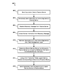
one striping
scheme, the application data may be written to write pages in each of eight
flash memory dice in
a RAID stripe, where the size of a write page is 8 KB. Therefore, effectively
the smallest unit
that can be written to a RAID-striped flash memory device may be on the order
of 8X8 KB, that
is, 64KB, or more.
[0069] In some implementations, a physical region of a flash memory
device may be
logically identified as a flash segment, also referred to as a segment. A
flash segment is an
aggregation of one or more erase blocks times the width of the RAID stripe.
For example, a
segment may span two erase blocks in each flash memory die in a RAID stripe.
The size of an
erase block may be about 2 MB and the RAID stripe may include eight flash
memory dice.
Therefore, the size of a segment is about 32 MB.
[0070] In some implementations, a flash segment is the granularity at
which areas of a
flash memory device are erased and managed. When new application data are
received, the flash
memory device writes one physical block, then the next physical block, then
the next physical
block, until some portion of the memory device is filled up, and then the
memory management
performs garbage collection on previously filled-in portions of the flash
memory dice.
[0071] When garbage collection is performed on a portion of flash memory
dice, the
system relocates the valid data out of that portion, erases the associated
blocks and places the
memory portion back into service so that it is able to receive new writes. The
segment is the
minimum unit at which level the flash management layer erases portions of the
flash memory
dice. Although physically flash can be erased at the level of erase blocks,
flash management
layer uses a segment since that allows more than one erase block to be erased
at a time.
[0072] In this context, the flash management layer is synonymous with the
flash
translation layer, which includes a collection of hardware and software logic
that are configured
to manage the physical locations in the flash memory device, such as the flash
memory dice, and
interface the physical memory with higher level applications and the operating
system. In some
implementations, the flash management layer includes a master controller for
managing the flash
CA 02905355 2015-09-10
WO 2014/151986 PCT/US2014/026773
17
memory dice, and several slave controllers, each of which are associated with
a subset of the
flash memory dice.
[0073] The flash management layer also includes software embedded in the
flash
memory device (that is, firmware) such as the flash translation table. The
granularity at which
DRAM pages or file system blocks get managed in flash memory die devices is
commonly
referred to as a translation unit, which is a logical construct specific to
the implementation of the
flash management layer for the flash storage device. The translation table
maps a logical block
address (LBA) to a physical block number (PBN), denoting a physical flash
location. The flash
management layer maintains the translation table internally, usually at a
fixed block granularity,
that is, fixed-size LBAs are mapped to fixed-size PBNs. This fixed granularity
of translation is
referred to as the translation unit. The overall system may be made more
efficient by selecting
the translation unit to be the same size as the expected data access size from
applications or the
operating system. At the level of applications and operating systems that
store data in flash
memory devices, the natural block size of data access falls into several
categories, with one
common size being 4 KB. Therefore, in some implementations, the translation
unit is configured
to be 4 KB in size.
[0074] In some implementations, header information may be associated with
each
segment. The header information may be a sequence number. For example, the
flash memory
dice may be managed as segment number 1, segment number 2, segment number 3,
and so on.
By associating a sequence number with each segment, the flash management can
effectively
associate with each segment the time order in which it was placed into service
in order to receive
new writes. Consequently, depending on which segment a write page belongs to,
the flash
management may determine that a write page in a segment with a lower sequence
number was
written before a write page in a segment with a higher sequence number. This
generates a time
order for write pages in flash memory dice as to when they got written, which
is referred to
previously as the flash memory device being written in a log manner, since a
log is normally
written in sequence from the beginning of the log onward.
[0075] At a point in time, some segments in a flash memory device are
completely
written, there are some segments that are being actively written, and there
are some segments
that are in clean state and they have not yet been written at all. The
sequence number or the set
of sequence numbers of the active segments in the memory system may be
considered to mark
CA 02905355 2015-09-10
WO 2014/151986 PCT/US2014/026773
18
the application data most recently stored in the memory device, since active
segments are
segments whose write pages are being actively written.
[0076] The flash memory device may include higher-level logic modules
that are
configured for managing the synchronous mirroring operations. For example, the
active and the
passive servers may include a higher-level software driver that manages data
mirroring between
the two ends, and partial synchronization of the data when one of the servers
recovers from a
failure mode. The higher-level software driver may interact with the flash
management layer for
managing the synchronous mirroring operations.
[0077] At certain times, the higher-level software driver query the flash
management
modules for information on the active segments. The trigger for the query may
be time-based,
for example, the query may be made periodically. Alternatively, the trigger
for the query may be
based on the amount of physical memory that has been written. For example, a
query may be a
based on a threshold number of segments that are written since the last query.
[0078] Based on the query from the higher-level software driver, the
flash management
layer determines the sequence number of the most-recently written segments and
the memory
blocks within the segments at the point in time, for example, time T1. The
flash management
layer sends the information to the higher-level software driver. After more
time has elapsed,
new writes came into the system and got stored in regions of the flash memory.
At time T2, the
flash management layer gets a new query from the higher-level software driver
and accordingly
sends the information on the most-recently written segments/memory blocks
within the segments
at time T2.
[0079] By examining the sequence numbers corresponding to the two
different points in
time, the higher-level software driver can determine the segments and memory
blocks that were
not written at T1 but written at T2 and, specifically, which write pages
include the write
operations performed in the time interval T2-T1.
[0080] For instance, at time T1 a flash memory device had one active
segment with the
sequence number was 37, which is sent to the higher-level software driver. At
time T2, the
sequence number of the active segment is 42. By reading the sequence numbers
corresponding
to T2 and T1, the higher-level software driver can determine that segments 37,
38, 39, 40, and 41
have been completely written during the time interval T2-T1, and segment 42 is
partially written.
The flash management can determine the physical locations in the flash memory
dice where the
CA 02905355 2015-09-10
WO 2014/151986 PCT/US2014/026773
19
segments 37, 38, 39, 40 and 41 reside, since only the memory blocks included
in the segments
37, 38, 39, 40 and 41 may have changed in the period T2-T1.
[0081] Therefore, by keeping track of sequence numbers associated with
active
segments, the flash management layer and the higher-level software driver may
obtain
information that is same as the information provided by the combination of a
disaster recovery
log and the un-committed write log, since the sequence numbers identify the
flash memory
blocks that may have been modified during a given time interval.
[0082] Methods, systems and devices are described in the following
sections for
synchronous mirroring in flash memory devices using sequence numbers
associated with flash
segments. For the purposes of this discussion, the terms "flash memory die,"
"flash memory
chip" and "flash memory" are used synonymously. The terms "active server,"
"local storage
element" and "local end" are used synonymously. Similarly, the terms "passive
server," "remote
storage element" and "remote end" are used synonymously. In addition, though
the remaining
sections are described in reference to flash memory devices, the techniques
described here may
be equally applicable to other forms of memory devices with aspects of
asymmetric behavior.
For example, phase change memory devices may be configured to employ these
operations.
[0083] Figure 1 illustrates an example of a system 100 that uses flash
memory for storing
data. The system 100 may implement techniques for synchronous mirroring of
data to flash
memory devices using sequence numbers associated with flash segments.
[0084] The system 100 includes one or more computer subsystems 102 that
are
interconnected by a network 104. A computer subsystem 102 includes one or more
servers such
as 106A, 106B and 106C through 106N.
[0085] Each computer subsystem 102 may be a server rack that hosts an
array of servers,
such as 106A, 106B, 106C and 106N. This may be the case, for example, when the
system 100
is a server farm or a back end processing center for an enterprise. The
computer subsystems may
be co-located at one physical location, such as in a data center, or they may
be geographically
distributed.
[0086] The computer subsystems 102 communicate with each other and with
remote
computers via the network 104, which may include a circuit-switched data
network, a packet-
switched data network, or any other network able to carry data, such as
Internet Protocol (IP)-
based or asynchronous transfer mode (ATM)-based networks, including wired or
wireless
CA 02905355 2015-09-10
WO 2014/151986 PCT/US2014/026773
networks. The network 104 may be a Local Area Network (LAN) or a Wide Area
Network
(WAN). The network 104 may include the Internet, analog or digital wired and
wireless
networks (such as IEEE 802.11 networks, Public Switched Telephone Network
(PSTN),
Integrated Services Digital Network (ISDN), and Digital Subscriber Line
(xDSL)), Third
Generation (3G) or Fourth Generation (4G) mobile telecommunications networks,
a wired
Ethernet network, a private network such as an intranet and/or any other
delivery or tunneling
mechanism for carrying data, or any appropriate combination of such networks.
In addition, the
network 104 may be configured to handle secure traffic such as secure
hypertext transfer
protocol traffic (HTTPS) or virtual private networks (VPN) such that the
connections between
the computer subsystems 102 may be secure connections, such as using VPN or
HTTPS.
However, in other implementations, the connections may be unsecured
connections.
[0087] Each server 106A, 106B, 106C or 106N is a computing device that
includes
memory modules for storing data, such as hard drives and flash memory. The
flash memory may
be in the form of memory cards on which multiple flash memory chips are
affixed. A flash
memory card may be organized into multiple memory packages or die packages,
also referred
simply as packages. A package is a multi-chip module that includes flash
memory dice. Each
flash memory die may be composed of flash planes that include constituent
blocks of memory
cells where data are stored. In some implementations, a die with two planes
has two distinct sub-
regions, each sub-region with its own memory array and interface circuitry.
The die has a
demultiplexing structure that sends commands to one plane or the other (or in
some cases, to
both planes). The memory cells may be single-level cells (SLCs), which store a
binary digit (bit)
corresponding to the value of the data that is stored in the particular memory
cell. Alternatively,
a memory cell may be a multi-level cell (MLC), which are configured to store
several bits
corresponding to the value of the data stored in the logical write page
locations associated with
the particular memory cell.
[0088] Each server may include multiple instances (for example, up to 16
to 24) of such
flash memory cards that are connected to a motherboard in the server, yielding
total flash
memory capacity that may vary in range from 0.5 terabyte (TB) for a smaller
memory card or
system to around 100 TB capacity for a larger memory card. From the
perspective of a flash
memory card, the server in which the memory card is included may be considered
as the host
system for the memory card. Therefore, based on the above exemplary figures,
the total capacity
CA 02905355 2015-09-10
WO 2014/151986 PCT/US2014/026773
21
of the host system may range from 0.5 TB to 100 TB, multiplied by the number
of cards in the
system.
[0089] In some implementations, some of the servers 106A, 106B, 106C or
106N may be
configured as active servers or as passive servers for a synchronous mirroring
set up. For
example, server 106A may be an active server that is connected, via the
network 104, to a
passive server at a remote computer subsystem 102, or to several passive
servers at one or more
remote computer subsystems 102. As another example, server 106A may be an
active server that
is connected to server 106C as a passive server in the same subsystem 102, or
to several servers,
such as 106B and 106C, as passive servers.
[0090] As mentioned previously, flash memory is a form of NVRAM, which is
a type of
random-access memory that retains its information when power is turned off
(hence, non-
volatile). This is in contrast to DRAM and static random-access memory (SRAM),
which both
maintain data only for as long as power is applied. NVRAM has asymmetric
properties, in
which the constituent operations, such as memory reads, writes, or erases,
differ from each other
by one or more orders of magnitude. For example, memory reads are performed
within the same
order of magnitude as the operations are performed in DRAM, memory write
operations are
performed much slower in comparison, and erase operations have even bigger
limitations.
Furthermore, certain types of NVRAM modules may have a limited number of
writes. This may
be the case, for example, due to the physical characteristics present in some
types of NVRAM
information storage mechanisms, which allow each NVRAM physical cell to be
programmed
and/or erased a limited number of times. Different types of NVRAM may have
different analog
properties (the underlying "noisy media" characteristics) depending on the
underlying physical
mechanism and density of the memory cell.
[0091] Each server also includes processors for processing data stored in
the memory
modules. In some implementations, the processors are present in the host
system, for example,
in the motherboard in the server to which the memory cards are coupled. In
such
implementations, the management of the flash memory may be performed by the
host system. In
some other implementations, one or more processors may be embedded in the
flash memory
cards. In such implementations, the management of the flash memory may be
performed by the
processors embedded in the memory card itself, or by some suitable combination
of the
processors embedded in the memory card and the processors in the host system.
CA 02905355 2015-09-10
WO 2014/151986 PCT/US2014/026773
22
[0092] The processors may be configured to execute instructions that are
stored in the
flash memory or elsewhere, such as in read-only memory (ROM). The instructions
may include
instructions for processing the data, for performing data striping at the
granularity of sub-sections
of flash memory chips, for recovering data stripes with degraded memory
sections by
dynamically re-striping the sections of flash memory chips that include
degraded regions.
[0093] Each server also may include DRAM for temporary storage of data
during
processing operations. In addition, each server includes network interfaces
for communicating
with other servers on the same computer subsystem 102 or in other computer
subsystems or
remote computers.
[0094] Figures 2A-2B illustrate an example of a memory device 200 that
includes flash
memory dice. The memory device 200 may be included, for example, in a server
in the system
100, such as one of servers 106A, 106B, 106C and 106N. However, the memory
device 200 also
may be included in other systems.
[0095] Figure 2A shows a schematic of the memory device 200 viewed from
one side.
As shown, the memory device 200, which is a memory card, includes a baseboard
202 with a
host edge connector 204. A master controller 206 is mounted on the baseboard
202. Also
mounted on the baseboard 202 are one or more memory packages, such as packages
212-232.
[0096] The baseboard 202 is a printed circuit board (PCB) that includes
one or more
layers of printed circuit board traces for interconnecting the various
components of the memory
card 200, including the master controller 206 and the different packages 212-
232. The baseboard
202 may be of a form factor that allows the memory card 200 to be included
within the chassis of
a server, such as 106A, 106B, 106C or 106N. In some implementations, the
baseboard 202 may
be configured to support a daughter board, which may be used to expand the
memory capacity of
the memory card 200. For example, the baseboard 202 may include sockets to
which a daughter
board may be coupled. The daughter board may include a number of memory
packages that are
similar to the packages 212-232, thereby increasing the total memory capacity
of the memory
card 200.
[0097] The host edge connector 204 is adapted to couple to sockets
mounted to a
motherboard of the host system. For example, the connector 204 may couple the
memory card
200 to the motherboard included in any of the servers 106A, 106B, 106C or
106N. The,
connector 204 is a computer data bus connector that is configured for
transferring data between
CA 02905355 2015-09-10
WO 2014/151986 PCT/US2014/026773
23
the memory card 200 and the host system. For example, the connector 204 may be
a Peripheral
Component Interconnect (PCI) bus, a PCI-eXtended (PCI-X) bus, a PCI Express
(PCIe)
computer expansion bus, or some other suitable connector.
[0098] The master controller 206 is a processing device that is
configured for managing
the storage and retrieval of data in the flash memory chips included in the
memory card 200. In
some implementations, the memory card 200 includes multiple master controllers
206. In some
implementations, the master controller 206 manages one or more slave
controllers that are
included in the packages 212-232 and coupled to the master controller 206 by a
plurality of
master-slave memory bus channels. In some other implementations, the slave
controllers are
included in the same logical unit (such as a package) as the master
controller, while retaining the
logical differences between the master and slave controllers. In yet other
implementations, the
master controller 206 manages one or more slave controllers that are external
to the packages
212-232. For example, the slave controllers may be placed between the master
controller(s) and
the flash memory dice. The master controller(s) communicate with the slave
controllers through
master-slave memory bus channels. Each slave controller in turn communicates
with a subset of
the flash memory dice, using, for example, a separate channel controller to
control each die.
[0099] A host bus channel formed of traces of the baseboard 202 may
couple the master
controller 206 to the host edge connector 204 for communicating with the host
system. The one
or more slave controllers are adapted to provide transparent access to the
flash memory included
in the packages. The master controller 206 and the slave controllers provide
native access of the
flash memory to the processors in the host system.
[0100] Each of the packages 212-232 includes a rectangular printed
circuit board on
which is mounted a plurality of packaged flash memory chips. The flash memory
chips may
include NAND flash memory die, NOR flash memory die, or any other suitable non-
volatile
memory. In some implementations, each of the packages 212-232 may have
different types of
flash memory that can be identified to the memory card 200 so that read
operations, write
operations, and/or erase or maintenance operations can be tailored to the
given type of memory.
[0101] In some implementations, each package includes 8 NAND flash memory
dice,
which are arranged in 4 pairings based on electrical wiring and pin outs that
come out of the
package, among other parameters. The two dice in a pair may be referred to as
siblings of each
other. The package is configured such that for each pair, one of the dice may
be active for
CA 02905355 2015-09-10
WO 2014/151986 PCT/US2014/026773
24
performing input/output (I/0) operations at a time, even though both dice may
be considered
active from a flash operation point of view. Therefore, in a package, 4 of the
dice may perform
input/output (I/0) operations concurrently, but all 8 dice may be active for
performing flash
operations.
[0102] In the above implementations, in addition to the 12 packages 212-
232 that are
shown, the memory card 200 includes 12 more packages mounted on the reverse
side of the
baseboard 202, yielding a total of 24 packages mounted on the baseboard 202.
In addition, the
memory card 200 includes the daughter board, with 24 packages mounted on the
daughter board.
Therefore, in such implementations, the total number of packages in the memory
card 200 is 48.
For 8 dice per package, the above configuration yields a total of 384 flash
memory dice in the
memory card 200.
[0103] In alternative implementations, the number of packages 212-232 may
be other
than 12, for example, some tens of packages, and the memory card 200 may
include additional
tens of packages mounted on the reverse side of the baseboard 202, yielding a
total number of
packages per board that is a number other than 24. With multiple boards per
card, such as one or
more daughter boards, the total number of packages in the memory card may be
in the tens or
hundreds, leading to multiple hundreds or thousands of dice.
[0104] In addition to the features shown in Figure 2A, the memory card
200 may include
one or more embedded processors, ROM, DRAM and additional NVRAM that are
mounted to
the baseboard 202. The ROM may be configured to store boot instructions for
the memory card
200. The DRAM may be configured to provide scratch pad memory to the embedded
processors
and store translation structures (for example, a translation table mapping
logical addresses to
physical addresses) to access data in the flash memory chips. The NVRAM may
include
firmware instructions for the memory card 200 that may be periodically
upgraded. The firmware
instructions drive and control the master controller 206 and the and slave
memory controllers to
perform read, write, erase or maintenance operations to access data with the
flash memory chips
of the packages 212-232. The embedded processors execute the firmware
instructions to drive
and control the master and slave memory controllers to access data as well as
read, write, and
maintain the translation structures in the DRAM.
[0105] The embedded processors may be further coupled to the master
memory
controller 206 and the edge connector 204 to communicate with each. The
embedded processors
CA 02905355 2015-09-10
WO 2014/151986 PCT/US2014/026773
also may be in communication with the host processors in the host system over
the edge
connector 204 to receive read and write operation requests from the host
application or host
operating system software to access data in the flash memory dice in the
memory card 200.
[0106] As described previously, each memory card 200 may have two types
of logical
controllers, namely, the master controller, which handles host-level
interactions, and slave
controller(s), which handles flash-level interactions. The master controller
and the slave
controller(s) may communicate using standard protocols, or a proprietary
hardware interface, or
any suitable combination of both. In some implementations, this interface is
implemented using
pins on the physical devices and traces on the baseboard. In other
implementations in which
master controller and slave controller(s) are in the same physical device, the
interface may be
implemented using internal device logic on the physical device.
[0107] In some implementations, a memory card 200 may utilize two
physical devices -
each of which implements one master controller and several slave controllers.
One of the master
controllers may be on the "baseboard" on the PCI expansion slot on the mother
board of the
computing device, and the other master controller may be On the "daughter
board" located on an
expansion slot on the baseboard. Communication between the host and the
daughter board's
master controller may be routed through the baseboard's master controller. In
such
implementations, communication between the two master controllers may be
through the
standard interface of PCIe. A proprietary hardware interface also may be
feasible.
[0108] The master controller(s) and slave controller(s) coordinate their
respective actions
to implement the data path of the flash memory system. In this context, the
data path, which also
may be referred to as the data plane, indicates that that the master and slave
controllers do not
themselves determine which flash memory locations are involved in the memory
operations.
Instead, the determination is made by the control path or control plane of the
system. The master
and slave controllers receive commands from the "control path" to perform
flash-level operations
and carry out such operations against specified host DRAM resources.
[0109] The control path of the system may be implemented by the driver
software, which
may be implemented as firmware instructions executed by the host processor or
embedded
processors associated with the controllers. In some implementations, there may
be a single
driver per card, while in other implementations; there may be several drivers
per memory card.
CA 02905355 2015-09-10
WO 2014/151986 PCT/US2014/026773
26
The driver software instructions may enable each slave controller to
communicate independently
with the master controller(s).
[0110] In some implementations, the driver software runs on the host
computing device
as a device driver. The device driver communicates with the master
controller(s) on the memory
card using standard PCIe commands ¨ in standard terminology, the latter may be
referred to as
"memory mapped I/0" (MMIO) instructions (they are load/store instructions at
the processor
level, except that they get routed to the appropriate device instead of DRAM).
The driver in turn
receives requests from host central processing unit (CPU) applications and
operating system (for
example, the file system component) using standard host-based application
programming
interfaces (APIs) and mechanisms (for example, a system call).
[0111] In some other implementations, the driver software runs on an
embedded
processor coupled with the baseboard master controller. In these
implementations, the term
"firmware" is usually used to denote the driver software. In still other
implementations, the
driver functionality may run in a split/parallel fashion across more than one
embedded processor
associated with one or more master controllers. In cases where the firmware
runs on one or more
embedded processors, the applications/operating system requests get
communicated to the
firmware using the same PCIe memory mapped I/0 instructions, using an
intermediate (separate,
minimal) software driver, for example, installed on the host computing device.
[0112] As described previously, the combination of the master controller,
the slave
controller(s) and the driver software may be referred to as the flash
translation layer or the flash
management layer. The flash management layer manages the flash memory dice,
for example,
mapping logical memory blocks to physical locations in the flash memory dice
using the flash
translation table. The flash management layer also interfaces the flash memory
dice with higher
level applications, such as the synchronous mirroring modules, and the
operating system.
[0113] Figure 2B illustrates a schematic of the memory card 200 showing
the flash
memory dice included in the packages 212, 214 and 232, which are a subset of
the packages 212-
232. Package 212 includes flash memory dice 212A...212N, package 214 includes
flash memory
dice 214A...214N and package 232 includes flash memory dice 232A...232N. Each
of the dice
212A...212N includes a slave controller, such as 212A(i)-212N(i) and memory
blocks 212A(ii)-
212N(ii) respectively. Each of the dice 214A...214N includes a slave
controller, such as
214A(i)-214N(i) respectively, along with memory blocks 214A(ii)-214N(ii)
respectively.
CA 02905355 2015-09-10
WO 2014/151986 PCT/US2014/026773
27
Similarly, each of the dice 232A...232N includes a slave controller 232A(i)-
232N(i) respectively
and memory blocks 232A(ii)-232N(ii) respectively.
[0114] Although FIG. 2B shows the slave controllers 212A(i)-212N(i),
214A(i)-214N(i)
and 232A(i)-232N(i) are mounted to the packages 212-232 and coupled between
the master
controller 206 and the plurality of flash memory dice, in some other
implementations, the slave
controllers 212A(i)-212N(i), 214A(i)-214N(i) and 232A(i)-232N(i) are mounted
to the baseboard
202 and coupled between the master controller 206 and the respective flash
memory dice in the
packages 212-232. In yet other implementations, the slave controllers 212A(i)-
212N(i),
214A(i)-214N(i) and 232A(i)-232N(i) are mounted together in an integrated
circuit package with
the master controller 206 and coupled between the master controller 206 and
the respective flash
memory dice in the packages 212-232.
[0115] Each slave controller is configured for providing transparent
access to its
respective die. As described previously, all the slave controllers are
connected to the master
controller 206 by a plurality of master-slave memory bus channels, which may
be implemented
as PCB traces on the baseboard 202. The master controller 206 natively
controls the flash
memory dice to obtain predictable bandwidth and latency performance with the
flash memory
dice included in the packages 212-232. All operations that take place on the
flash memory dice
212A...212N, 214A...214N or 232A...232N (for example, read, write, erase,
control operations
such as reset, etc.) are completely visible to (and under the control of) the
master controller 206.
The flash memory interface of active dice of the dice in a package is passed
through the
respective slave memory controller to the master controller 206. For example,
the flash memory
interface of the die 212A is passed through the slave controller 212A(i) to
the master controller
206.
[0116] The master controller 206 is able to exercise directly each of the
operations that
are supported by the flash memory dice 212A...212N, 214A...214N or
232A...232N. The slave
controllers may perform protocol conversion, but do not drop/intercept
(without involving the
associated flash memory die) a request from the master controller. However,
the slave
controllers do not autonomously initiate any flash memory operation.
[0117] Each slave controller 212A(i)-212N(i), 214A(i)-214N(i) and 232A(i)-
232N(i) is
configured to arbitrate memory bus channels shared by the multiple flash
memory dice
212A...212N, 214A...214N and 232A...232N respectively. Each slave controller
can buffer and
CA 02905355 2015-09-10
WO 2014/151986 PCT/US2014/026773
28
multiplex signals between the master controller 206 and the multiple flash
memory dice. In
addition, each slave controller can combine a sequence of predictable non-
volatile memory
operations together into a compound operation to improve control bandwidth
with the flash
memory dice.
[0118] The granularity at which the data in the flash memory dice 212A..
.212N,
214A...214N and 232A...232N is accessed may be referred to as memory blocks or
memory
pages. For example, the flash memory die 212A includes multiple memory blocks
that are
indicated collectively by 212A(ii) in Figure 2B. The size of a memory block
may vary based on
the type of flash memory that is used. For example, the size of a memory block
may be different
for NAND flash dice and NOR flash dice. Among NAND flash devices, the sizes
may be
different between SLC and MLC types of NAND flash. NAND flash from different
process
generations also may have different sizes (for example, 34nm NAND flash versus
25nm NAND
flash). In addition, the size of a memory block may vary based on the type of
operation that is
performed on the flash memory device. For example, for a NAND flash memory
device, data
may be written to the memory device in units of write pages. The size of a
write page may be
small, in the order of a small number of kilobytes (e.g., in the range 4KB ¨
16KB).
[0119] In some implementations, data may be erased from the NAND flash
device in
units of erase blocks, which are typically larger in size than the write pages
(in the order of
several megabytes) and one erase block may include multiple write pages. Once
data is written
to a write page, the entire erase block associated with the write page has to
be erased before new
data can be written to the write page. In some other implementations, data may
be erased in
units of flash segments as described previously. A flash segment is a logical
construct mapping
to a physical region of a flash memory card 200 that is composed of multiple
erase blocks
distributed across the flash memory dice in a RAID stripe.
[0120] Figure 3 illustrates an example of a memory page 300 that is
stored in a flash
memory die. The flash memory chip may be one of 212A...212N, 214A...214N and
232A.. .232N that are packaged in the memory card 200. However, the flash
memory chip also
may be implemented in other memory cards or systems.
[0121] The memory page 300 includes a data portion 302 and an error
correction code
(ECC) portion 304. The data portion 302 includes memory units 302a-302h in
which data is
stored. The memory page has a page starting address indicated by 306.
CA 02905355 2015-09-10
WO 2014/151986 PCT/US2014/026773
29
[0122] The size of the data portion may vary depending on the particular
NVRAM
design and configuration. In the example shown, the data portion 302 has a
size of 4 KB. Other
sizes for the data portion may be used (for example, 8 KB or 16 KB).
[0123] As shown in FIG. 3, the memory page 300 has an offset address
indicated by zero
through seven from the page starting address 306, which allows each of the
memory units 302a-
302h to be 512 bytes in size. In some implementations, each of the memory
units 302a-302h
may correspond to a write page, while the data portion 302 may correspond to
an erase block.
Therefore, in such implementations, the erase block 302 includes the write
pages 302a-302h.
[0124] The size of the ECC varies with the underlying NVRAM
implementation. For the
configuration where the data portion 302 is 4 KB, the ECC portion 304 is 128
bytes. In other
implementations, the size of the ECC portion may be higher (such as in the
range of 500 bytes)
to meet the higher media error rates of data portions of larger size (for
example, for more current
generations of flash devices such as MLC type memory).
[0125] The ECC portion 304 is used to store ECC data that is used for
error correction of
data stored in 302a-302h. An error correction code may be generated for each
512 byte unit
302a-302h. Program write errors or flash read errors may be detected using the
error correction
code. While ECC is useful to correct an a priori anticipated threshold of bit
errors, redundant
data storage may be used to recover data when the number of bit errors exceeds
the a priori
threshold or due to a complete failure of a storage device, such as the flash
memory die in which
the memory page 300 is included.
[0126] In some implementations, data may be stored in one or more 512
byte regions
across a memory page with one or more consecutive offset addresses
respectively. The region in
which data is stored may be referred to as a chunk of memory. For example,
employing a single
offset address allows a 512 byte chunk of data to be stored across one of the
units 302a-302h of
the memory page 300. A RAID group in this case may be consistently written
with regions of
512 byte chunks of data. This may be the case, for example, with 7 data
stripes and lparity
stripe spread across 8 flash memory dice that implement 4 KB memory pages,
such as the page
300. In this configuration, each die sees a 512 byte region for each stripe
within the same
memory page.
[0127] In some other implementations, a pair of offset addresses (for
example, offset
addresses 6 and 7) may be used to allow 1 KB chunks of data to be stored in
regions of the
CA 02905355 2015-09-10
WO 2014/151986 PCT/US2014/026773
memory page 300. A RAID group in this case may be consistently written with
regions of 1 KB
chunks of data. This may be the case with three data stripes and one parity
stripe spread across
four flash memory devices with 4 KB memory pages, such as the memory page 300.
In this
configuration, each die sees a 1 KB region for each stripe within the same
memory page.
[0128] In some implementations, a software driver or embedded firmware
operating on
the host system may accumulate data, calculate parity, and store the data and
parity information
as stripes across the flash memory dice. The parity calculations may be
performed by the host
processors, for example, based on instructions of the host software driver or
embedded firmware.
In other implementations, the software driver operating on the memory card 200
may accumulate
the data and initiate a command to the master controller 206. The master
controller 206 can then
be responsible for computing the parity information and storing the data and
parity stripes across
the flash memory dice.
[0129] The memory card 200 may include several such RAID groups. For
example,
referring to the implementation of the memory card 200 with 48 packages with 8
dice per
package, the memory card 200 may include 24 RAID groups, with 16 dice in 2
packages in each
group.
[0130] Figure 4 illustrates an example of a group 400 of flash memory
dice storing data
redundantly in data stripes distributed across the group of flash memory dice.
The flash memory
dice may be mounted on the memory card 200. For example, the flash memory dice
may be
212A...212N, 214A...214N and 232A...232N that are packaged in the memory card
200.
Accordingly, the following sections describe the group 400 of flash memory
dice as
implemented by the card 200 in the system 100. However, the group 400 of flash
memory dice
also may be implemented by other memory cards and systems,
[0131] The group 400 illustrates one implementation of a RAID-aware flash
memory
layout. The group 400 includes N flash memory dice 402A, 402B, and 402C
through 402N,
collectively referred as 402A...402N. Pages of data are stored across the
flash memory dice
402A...402N in M data stripes 404A and 404B through 404M, collectively
referred as
404A.. .404M. Each stripe includes N data chunks, such as A0.. .AN for data
stripe 404A,
BO...BN for data stripe 404B and MO...MN for data stripe 404M. A parity stripe
406 is also
stored across the flash memory dice 402A...402N. The parity stripe is formed
of parity chunks
CA 02905355 2015-09-10
WO 2014/151986 PCT/US2014/026773
31
PA-PM and a single meta-data parity chunk PN. One or more of the data chunks
in a RAID
stripe are aggregated together to form a flash segment, such as segment 408.
[0132] It is to be noted that various configurations may be used other
than the
configuration shown. For example, different encoding of the parity stripe may
be used that
group the parity information across multiple data stripes. Similarly, the
parity information may
be stored as part of the individual data stripes instead of being stored in a
separate parity-only
stripe.
[0133] The flash memory dice 402A...402N may be same as the flash memory
dice
212A...212N, or 214A...214N, or 232A...232N. The size of each data chunk may
depend on the
number of flash memory dice that are used, and the number of data stripes.
Each data chunk
may have a size same as a write page, or an erase block, or some other
suitable size unit of
memory.
[0134] For each data stripe, a corresponding parity chunk is generated by
computing
parity of the data chunks included in the data stripe that are stored in the
flash memory dice. For
example, PA is the parity chunk for the data stripe 404A; therefore, PA may be
computed based
on the data chunks AO...AN. The meta-data parity chunk PN is parity computed
from the
plurality of parity chunks previously generated. Therefore, PN is computed
based on the parity
chunks PA.. .PN.
[0135] In some implementations, the parity chunks and the meta-data parity
chunk in the
parity stripe are selectively stored on different flash memory die so that
data can be recovered in
response to a failure, removal, and replacement of a flash memory die. Each
data chunk in a
stripe is also stored in a different flash memory die so that data can be
recovered in response to a
failure, removal, and replacement of a flash memory die. For example, for the
data stripe A, the
data chunk AO is stored in the flash memory die 402A, data chunk Al is stored
in the flash
memory die 40B, data chunk A2is stored in the flash memory die 402C, and the
data chunk AN
is stored in the flash memory die 402N.
[0136] The parity chunks and the meta-parity chunk can be stored
arbitrarily across the
flash memory dice 402A...402N provided their locations are known. For example,
as shown, the
PA chunk in the parity stripe 406 is stored in the flash memory die 402A, the
PB parity chunk is
stored in the flash memory die 402B, the PC parity chunk is stored in the
flash memory die
402C, and the meta-parity chunk PN of the parity stripe 406 is stored in the
flash memory die
CA 02905355 2015-09-10
WO 2014/151986 PCT/US2014/026773
32
402N. In another implementation, the meta-parity chunk PN may be stored in the
flash memory
die 402A, the PA parity chunk may be stored in the flash memory die 402B, the
PB parity chunk
may be stored in the flash memory die 402C, and the PC parity chunk may be
stored in the flash
memory die 402N.
[0137] As shown, M data stripes and one parity stripe are written across N
flash memory
dice 402A through 402N for each flash write page. The data and parity are
striped across
multiple write pages, erase blocks or some other suitable memory unit in the
different flash
memory dice. The data stripes and parity stripes are written to different
offsets within one or a
couple of flash write pages, erase blocks or some other suitable memory unit,
for each
constituent flash memory die. The parity chunk PA is a result of determining
the parity of the
data stripe 404A. The parity chunk PB is a result of determining the parity of
the data stripe
404B. The parity chunk PM is a result of determining the parity of the data
stripe 404M. PN
represents the parity meta-data chunk stored in a flash memory die 402N with
its value being the
parity of the parity data chunks PA through PM.
[0138] The system may be configured to be responsive to the relative size
of "data
chunk" sizes and the use of a particular data chunk size relative to the
impact on the system. A
data chunk may have a size equivalent to an erase block, or some other
suitable unit of size
associated with the memory. For example, each of AO...AN may correspond to an
erase block in
the respective flash memory die 402A...402N. In such cases, data associated
with the stripe
404A may be written to the erase blocks AO through AN in the flash memory dice
402A through
402N, respectively.
[0139] As described above, in striping, the data may be redundantly stored
in different
flash memory dice at the granularity of erase blocks, or some other suitable
unit of size
associated with the memory. For example, data that is striped in 404A in data
chunks of size
equivalent to erase blocks may be replicated in a different group of flash
memory dice. In some
implementations, the data may be redundantly stored using parity encoding,
such as XOR
encoding, as described previously. In some other implementations, the data may
be replicated
using mirroring, while in some other implementations, the data may be
redundantly stored using
some suitable combination of parity encoding and mirroring, and/or some other
appropriate
mechanisms.
CA 02905355 2015-09-10
WO 2014/151986 PCT/US2014/026773
33
[0140] In one configuration, the data chunks for a data stripe may be
written to 8 flash
memory dice. Referring to the example of a flash memory die package with 8
dice arranged in 4
pairings with one die of each pair active at a given time for I/0 operations,
the above
configuration may include the 4 active (considered from an I/0 operations
perspective) dice from
one package, such as 212, and 4 active dice from another package, such as 214.
The data chunks
written to the 4 active dice in a package may be replicated in the other 4
sibling dice in the
respective package. In this manner, the data may be striped and replicated to
provide RAID-like
reliability. In some implementations, depending on factors such as the
configuration of the slave
controller and channels relative to the number of memory dice, other
configurations may be
used. For example, the data chunks may be striped across 8 different dice in 8
different packages
along with parity encoding to provide the ability to reconstruct the data
chunks in the event of
the loss of any single die or package.
[0141] The group of flash memory dice that are involved in storing and
replicating data
in the above manner constitute a RAID group. As indicated previously, the RAID
group, also
referred to simply as a RAID, provides data reliability to the data stored in
the flash memory dice
402A...402N. In the present context, a RAID group is associated with a
collection of erase
blocks that are aligned at the same memory address offset for each flash
memory die in the
RAID group. In the above example, the RAID group constitutes 16 flash memory
dice across 2
packages. The RAID group has a "width" of 8, that is, data chunks in a data
stripe are stored
across 8 flash memory dice and replicated in 8 other flash memory dice.
[0142] The segment 408 includes one or more erase blocks in each flash
memory die in
the RAID group. For example, each of the data chunks AO...AN may be an erase
block as
discussed previously. The segment 408 may be composed of the erase blocks AO..
.AN, as
shown. In an alternative configuration, the segment 408 may be composed of two
erase blocks
per flash memory die, such as AO and BO in die 402A, Al and B1 in die 402B,
and so on. Data
is written to the flash memory dice 402A...402N sequentially in the order of
segments. Data is
written to a segment at the granularity of the write pages included in the
erase blocks within the
segment. Therefore, the write pages corresponding to the erase blocks in the
segment 408 are
filled up first before writing the to the write pages corresponding to the
erase blocks in the next
higher segment.
CA 02905355 2015-09-10
WO 2014/151986 PCT/US2014/026773
34
[0143] While writing the data to the segments, the flash management layer
keeps track of
the active segment, that is, the segment currently written. In some
implementations, the flash
management layer also keeps track of the write page and/or erase block within
the active
segment that is currently written.
[0144] A higher-level software driver, which is configured for managing
the synchronous
mirroring operation with a passive server, queries the flash management layer
at specific points
in time for information on the active segments. Upon receiving the query, the
flash management
layer determines the sequence number of the segment that is most-recently
filled, and the number
of the memory block within the segment that is most recently written to. The
flash management
layer sends the information to the higher-level software driver. The higher-
level software driver
in turn forwards the sequence number of the segment and the memory block
within the segment
to the passive server, which stores the information in a "marker," which is a
data structure that is
maintained by the higher-level software driver at the passive server. In some
implementations,
the active server may receive an acknowledgement from the passive server,
which indicates to
the active server that the remote end has received the updated information.
[0145] Figure 5 illustrates an example of a memory server 500 that
performs
synchronous mirroring using segment sequence numbers. The memory server 500
may be either
the active server or a passive server in a synchronous mirroring setup. The
memory server 500
includes as the storage element the memory card 501, which may be similar to
the memory card
200 included in the system 100. The memory card 501 includes a master
controller 502, which
manages the flash memory dice 504, 506, 50J and 50K Cr and `I(' being
integers) through the
slave controllers 514, 516, 51J and 51K respectively. The flash memory die 504
includes
multiple erase blocks, such as 504a, 504b, 504c, 504x, 504y and 504z.
Similarly, flash memory
die 506 includes multiple erase blocks, such as 506a, 506b, 506c, 506x, 506y
and 506z; flash
memory die 50J includes multiple erase blocks, such as 50Ja, 50Jb, 50Jc, 50Jx,
50Jy and 50Jz;
and flash memory die 50K includes multiple erase blocks, such as 50Ka, 50Kb,
50Kc, 50Kx,
50Ky and 50Kz. .
[0146] The flash memory dice 504, 506, 50J and 50K are part of a RAID
stripe that
includes segments 522, 524 and 52M, among others. The erase blocks in each
flash memory die
are split into different segments. For example, in flash memory die 504, erase
blocks 504a and
504x are in segment 522, erase blocks 504b and 504y are in segment 524, and
erase blocks 504c
CA 02905355 2015-09-10
WO 2014/151986 PCT/US2014/026773
and 504z are in segment 52M. For each segment, the memory card 501 stores the
sequence
number of the segment, and the erase block within the segment that is recently
written. In some
implementations, the memory card 501 may store the information in the flash
memory dice. For
example, the segment sequence number for segment 522 may be stored as 522a in
the flash
memory die 504, while the segment sequence number for segment 524 may be
stored as 524a in
the flash memory die 506. In some other implementations, the memory card 501
may store the
segment information separately from the flash memory dice, for example in an
on-board RAM.
[0147] The memory card 501 includes a flash translation table 530. The
flash translation
table 530 maps a logical block address (LBA) to a physical block number (PBN),
which
indicates the physical locations in one or more flash memory dice where the
data are stored. In
some implementations, the translation table may be a dynamic RAM (DRAM)
structure that is
distinct from the flash memory dice 504...50K. However, in other
implementations, the
translation table may be stored in a dedicated portion of one or more flash
memory dice, or in
some other suitable location.
[0148] The master controller 502, the slave controllers 514, 516, 51J and
51K and the
flash translation table 530 together constitute the flash management layer for
the memory card
501. In implementations where the memory server 500 is a passive server in the
synchronous
mirroring setup, the memory card 501 stores the information on active
segments, which is
received from the active server, using markers, such as marker A 542 and
marker B 544. The
markers may be stored in a separate memory structure 540, for example, RAM. In
addition, or
alternatively, the markers also may be stored in the flash memory dice.
[0149] The memory server 500 includes a synchronous mirroring module 550,
which is a
higher-level software driver that manages the mirroring operations for the
storage elements
associated with the memory server 500, for example, the memory card 501. The
synchronous
mirroring module 550 is implemented as part of the higher level software in
the memory server
500, outside the memory card 501.
[0150] Although Figure 5 shows three segments 522, 524 and 52M, the total
number of
segments in the memory card 501 may be a different number that is greater than
the three shown.
Further, although the segments are shown as composed of portions of the flash
memory dice 504,
506, 50J and 50K, the segments may include portions of other flash memory dice
that are not
shown. The number of erase blocks per flash memory die in a segment also may
be different
CA 02905355 2015-09-10
WO 2014/151986 PCT/US2014/026773
36
than the number shown. For example, in some implementations, each segment may
include only
one erase block per flash memory die. In some other implementations, different
segments may
include different number of erase blocks.
[0151] The flash memory dice 504, 506, 50J and 50K may belong to the same
package,
or they may belong to different packages. As described previously, in some
implementations,
the slave controllers 514, 516, 51J and 51K may be mounted to the packages
associated with the
flash memory dice 504, 506, 50J and 50K respectively and coupled between the
master
controller 502 and the respective flash memory dice. In some other
implementations, the slave
controllers 514, 516, 51J and 51K are mounted to the baseboard 501 and coupled
between the
master controller 502 and the flash memory dice in the associated packages. In
yet other
implementations, the slave controllers 514, 516, 51J and 51K are mounted
together in an
integrated circuit package with the master controller 502 and coupled between
the master
controller 502 and the flash memory dice.
[0152] As described previously, in some implementations, the flash
management layer
writes new data items to the flash media dice 504, 506, 50J and 50K in a
manner analogous to
writing a log. The flash management layer carves the total storage on each
flash memory die on
the memory card 501 into discrete units at the granularity of erase blocks and
physically
organizes collections of erase blocks in a RAID group into sequential
segments. For example,
for a RAID group of width 8 (that is, there are 8 flash memory dice in the
RAID group) and an
erase block (for example, 504a or 506a) size of 2 megabytes (MB), a segment
(for example, 522
or 524) may be of size 2 erase blocks x 8 wide x 2 MB/erase block, that is, 32
MB. Therefore,
the total storage in the memory card 501, which may be in the order of
terabytes, may be
organized into multiple segments, which are in the order of tens of megabytes.
[0153] When the flash management layer receives a write operation from
the higher-level
application or operating system, it identifies a current active segment,
writes the data associated
with the write operation in the next available location in the active segment,
and makes an
entry in the flash translation table that LBA X (for example, corresponding to
a write page in the
erase block 504a) has now been written to physical location Y (for example, in
flash memory die
504) that corresponds to active segment Z (for example, segment 522).
Therefore, the flash
management layer fills segments in a log manner with the application data and
fills entries in the
flash translation table in a log manner. Considering three writes
consecutively as Write 1
CA 02905355 2015-09-10
WO 2014/151986 PCT/US2014/026773
37
followed by Write 2 followed by Write 3, the data for Writes 1, 2 and 3 will
appear in log
manner in the segments, and the translation entries for the Writes 1, 2, and 3
will appear in log
manner in the flash translation table.
[0154] When space is no longer available for writing new data in the
physical flash
memory dice that maps to the current segment, the current segment is said to
fill up with data,.
The flash management layer marks another segment as being active and then
effectively
performs the same operation as described in the preceding section. In some
implementations,
there may be more than one active segment for efficiency reasons. The flash
management layer
will route a write request to one of the active segments.
[0155] When a segment is activated for storing data, the flash management
layer
associates a sequence number with the segment. In some implementations, the
sequence number
is the next higher sequence number after the segment that was written
immediately prior to the
currently activated segment. In some other implementations, sequence numbers
are in
descending order such that the sequence number associated with a segment is
the next lower
sequence number after the segment that was written immediately prior to the
currently activated
segment.
[0156] In some implementations, the sequence numbers of the segments may
be recorded
in the physical flash memory, associated with the corresponding segment. For
example, the
sequence number for segment 522 may be recorded in a portion 522a of the flash
memory die
504, while the sequence number for segment 524 may be recorded in a portion
524a of the flash
memory die 506. In some other implementations, the sequence numbers of the
segments may be
recorded in a separate memory other than the flash memory dice, such as in a
RAM.
Alternatively, the sequence numbers of the segments may be recorded both in
the flash memory
dice (for example, 522a or 524a) and in a separate RAM.
[0157] In some implementations, for the active segments, along with the
sequence
numbers of the segments, the flash management layer records the sequence
number of the next
available flash memory block (for example, write page) within the active
segment in the physical
flash memory dice (for example, 522a or 524a), or in a separate memory (for
example, RAM), or
both. The sequence numbers of the flash memory blocks within a segment may be
recorded as
offsets from first memory block within the segment. For example, if there are
4096 write pages
CA 02905355 2015-09-10
WO 2014/151986 PCT/US2014/026773
38
within the erase blocks included in a segment, the write pages may be
sequentially marked 0-
4095, with 0 being the number of the first write page in the segment.
[0158] The flash management layer records information on the active
segments
separately so that the active segments may be tracked apart from the non-
active segments. For
example, the flash management layer may maintain a record in DRAM that stores
the sequence
numbers of the active segments. Therefore, when new segments become active,
the sequence
numbers that are stored in the DRAM record for the active segments are
updated.
[0159] The synchronous mirroring module 550 queries the flash management
layer for
information on the active segments at points in time. In response to the
query, the flash
management layer may send the sequence number(s) of the active segment(s), and
the offset(s)
within the active segment(s) that denote the sequence number(s) of the next
available flash
memory block(s) within the active segment(s).
[0160] The synchronous mirroring module 550 forwards the sequence
number(s) of the
active segment(s) along with the sequence number(s) of the next available
flash memory block(s)
within the active segment(s) to the passive server in the synchronous
mirroring setup. The
passive server stores the information received from the active end in data
structures called
markers. For example, if the memory server 500 is a passive server, then the
memory server 500
stores marker 542 that provides information on the sequence number(s) of the
active segment(s)
and the sequence number(s) of the next available flash memory block(s) within
the active
segment(s) at the active end. As shown, marker 542 includes the sequence
number and block
number of an active segment on the active server. There may be two active
segments on the
active server at a time; therefore, the marker 542 may store information on
the sequence numbers
of both active segments, and, for each active segment, the sequence number of
the next available
flash memory block within the segment.
[0161] In some implementations, the passive server may store more than
one marker.
For example, if the memory server 500 is a passive server, then the memory
server 500 may
store two markers 542 and 544 as shown. This may be useful in the two-level
marker scheme,
which is described in a following section. In such implementations, each of
the two markers 542
and 544 provides information on the sequence number(s) of all the active
segment(s) and, for
each active segment, the sequence number of the next available flash memory
block within the
CA 02905355 2015-09-10
WO 2014/151986 PCT/US2014/026773
39
active segment at the active server corresponding to the writing phase
associated with the
respective marker.
[0162] The marker may be considered as metadata associated in the flash
management
layer. In some implementations, the markers may be stored in memory separate
from the
physical flash memory, such as in a RAM 540. In some other implementations,
the markers may
be stored in the physical flash memory, for example, as data structures in a
known portion of the
flash memory dice 504, 506, 50J or 50K. In other implementations, the markers
may be stored
both in the physical flash memory and in a separate memory such as a RAM.
[0163] The markers 542 and/or 544 are periodically updated on the passive
server when
the synchronous mirroring module on the active server sends updated
information regarding the
active segments on the active server. In some implementations, the markers are
managed by the
synchronous mirroring module on the passive server, while in some other
implementations, the
markers are managed by the flash management layer on the passive server. In
other
implementations, the markers are managed by a suitable combination of the
synchronous
mirroring module and the flash management layer on the passive server.
[0164] A marker is equivalent to recording a position in a logical log.
Given two
positions in the logical log, the entries that were written in the log between
those two positions
can be determined. Therefore, given two markers, the synchronous mirroring
module can
identify which are the flash memory blocks (for example, write pages) that got
written between
in the time period that happened between the two markers. Knowing the physical
flash memory
blocks that got written, the synchronous mirroring module can query the flash
management layer
for information on the logical memory blocks corresponding to the determined
physical blocks.
[0165] The flash management layer maintains the mapping between logical
memory
blocks and the physical memory blocks that got written using the flash
translation table 530.
Based on information from the markers, the synchronous mirroring module asks
the reverse
question, that is, what is the logical memory block that the physical flash
block corresponds to,
given the physical flash block that got written.
[0166] In some implementations, using the information on the active
segments at the
active server and the markers stored in the passive server, the
functionalities of a disaster
recovery log and the un-replicated write log may be reproduced. The
synchronous mirroring
module 550 on the active server periodically queries (for example, every few
seconds) the flash
CA 02905355 2015-09-10
WO 2014/151986 PCT/US2014/026773
management layer on the active server on the sequence number(s) of the current
active segments
and the offset(s) for the next available memory block within the active
segment(s). The
synchronous mirroring module 550 sends the information to the passive server
on the other end
of the connection in the synchronous mirroring setup. The passive server
records the received
information as the latest marker value received from the active server.
[0167] When the synchronous mirroring system recovers from a crash, the
active and the
passive servers reach agreement upon the last marker that has been seen from
each other. In
some implementations, the synchronous mirroring module on the passive server
sends to the
active server the last marker that the passive server had received before the
crash. The
synchronous minoring module on the active server queries the flash management
layer on the
active server for the sequence number(s) of the active segment(s).
[0168] The synchronous mirroring module compares the sequence number(s)
of the
active segment(s) that are retrieved from the flash management layer with the
sequence
number(s) of the segment(s) indicated in the marker received from the passive
server. The
difference between the sequence number(s) corresponds to all the writes that
might have taken
place at the active server that are not replicated at the passive server.
Therefore, the active server
effectively has the disaster recovery log information.
[0169] The synchronous mirroring module on the active server queries the
flash
management layer to verify that the physical flash blocks corresponding to the
writes identified
above to continue to represent valid logical blocks. That is, the physical
flash blocks include
data that are mapped accurately by the corresponding logical blocks. This
check is performed
since situations may arise, for example, where a physical flash block was
erased and/or had new
data written to it, but the logical block that previously mapped to the
physical block was not
updated.
[0170] If the synchronous mirroring module verifies that the physical
flash blocks
corresponding to the identified writes continue to represent valid logical
blocks, then the
synchronous minoring module retrieves the writes and the logical memory blocks
corresponding
to the identified writes and sends them to the passive server. On the other
hand, if the
synchronous mirroring module determines that one or more physical flash blocks
corresponding
to the identified writes no longer represent valid logical blocks, then the
synchronous minoring
module does not send the associated writes or the incorrect logical memory
blocks. In such
CA 02905355 2015-09-10
WO 2014/151986 PCT/US2014/026773
41
cases, the synchronous mirroring module retrieves the remaining writes and the
corresponding
logical memory blocks (which continue to be valid) and sends them to the
passive server.
[01711 When the synchronous mirroring module on the active server sends
the active
segment sequence number information to the passive server, the system has to
ensure that there
is no write operation that got started before the information was sent, but
finished after the
information was transmitted. This may be regarded as a "write barrier," which
is needed for
correctness in that there cannot be operations that appear on both sides of a
marker because the
marker is used as a synchronization device.
[0172] Consider two user writes that were issued before synchronous
mirroring module
550 on the active server queries the flash management layer for information on
the active
segments, but the two user writes are not completed by the time the
information is sent from the
flash management layer. It may be possible that, with regard to the order in
which the two user
writes and the active segment information are communicated to the passive
server, the ordering
might be different from the ordering on the active server. One of the writes
might actually
happen before the active segment information is received ón the passive node,
while the other
write may happen after. Because there is the possibility of confusion in the
order on the active
server and the passive server, the synchronous mirroring setup may not be
correct because the
synchronous mirroring modules on the active server might wrongly interpret
both writes as
having been recorded on the passive server while in actuality only one of the
writes may have
been recorded. While performing recovery using the markers stored by the
passive server,
because the second write on the active server was performed before the active
segment
information was retrieved, as part of the recovery process, the second write
will not get shipped
to the passive server. The synchronous mirroring system will not be aware that
the write
operation was missed. Therefore, for synchronous mirroring using a marker-
based scheme to be
correct, write operations should be ordered strictly before and after the
retrieved marker
information on the active segment in order to remove the confusion of what
could have happened
with the writes that happened concurrently with the retrieving the marker
information.
[0173] In the implementation described in the previous section, the write
barrier may be
achieved by stopping the I/0 operations when the sequence number information
is being
collected and transmitted. The synchronous mirroring system ensures that all
writes operations
in the system have finished before the information on the active segments is
retrieved from the
CA 02905355 2015-09-10
WO 2014/151986 PCT/US2014/026773
42
flash management layer. New writes are not allowed in the system until the
marker information
has been retrieved, and then write operations are resumed. However, this may
generate
"hiccups" in the system in the context of performing I/0 operations. Both
stopping, waiting for
the writes to be finished and preventing new writes from proceeding until the
information has
been returned by the flash management layer may increase the response times.
For example, if
the information corresponding to the active segment(s) is collected every two
seconds, there is a
few milliseconds worth of time when the I/0 operations are not performed.
[0174] In some implementations, the write barrier may be achieved without
incurring
hiccups using a two-level marker scheme, which may be known as the red-black
marker scheme.
In such implementations, the write operations on the active server are
performed in phases, with
the write transactions on the active server categorized into one of two types,
which may be
referred to, for illustrative purposes, as a red phase (or red writing phase)
and a black phase (or
black writing phase).
[0175] The write operations are performed on the active server in the
order of a red
phase, followed by a black phase, followed by a red phase"and so on. While
performing a write
operation in the red phase, the flash management layer retrieves the
information for the segment
that was active in the last black phase. While performing a write operation
for the black phase,
the flash management layer retrieves the information on the active segment
corresponding to the
last red phase. Therefore, the synchronous mirroring system overlaps the
segment information
retrieval and the new write operations that are coming into the system.
[0176] In some implementations, when write operations are performed in
the black
phase, the flash management layer retrieves the sequence number(s) of the
segment(s) that are
active in the black phase (and the sequence number(s) of the memory blocks
within the active
segment(s) that are written) and stores them in the DRAM record for the active
segments with an
indication that the sequence number(s) being stored corresponding to the
active segments in the
black phase. Similarly, during write operations in the red phase, the flash
management layer
may store the sequence number(s) of the active segment(s) in the DRAM record
with an
indication that the sequence number(s) being stored corresponding to the
active segments in the
red phase. For example, if the memory server 500 represents an active server,
segment 522 may
have been the active segment in the black phase. Accordingly, the flash
management layer
stores in the DRAM record the sequence numbers of segment 522 and the memory
block within
CA 02905355 2015-09-10
WO 2014/151986 PCT/US2014/026773
43
segment 522 that was just written, indicating that the sequence numbers are
associated with the
black phase. At the next red phase, both segments 522 and 524 may be written.
The flash
management layer stores in the DRAM record the sequence numbers of segments
522 and 524
(along with the sequence numbers of the memory blocks within the respective
segments),
indicating that the sequence numbers are associated with the red phase.
[0177] In some implementations, the flash management layer may maintain
separate
DRAM records corresponding to the different phases. In such implementations, a
first DRAM
record may be used to store sequence numbers corresponding to the active
segments in the black
phase, while a second DRAM record may be used to store sequence numbers
corresponding to
the active segments in the red phase, and so on.
[0178] The property provided by the information on active segment(s)
retrieved by the
flash management layer is that the information is accurate up to the last
phase that it represents.
The information may not be accurate for the current write operations that are
performed while
the information is retrieved.
[0179] When a write operation corresponding to the red phase is being
performed while
the information on the active segment(s) corresponding to the black phase is
being retrieved, the
red phase write operation does not have to stop for the black phase active
segment information to
be retrieved. The write operation corresponding to the red phase may continue.
However, all
previous write operations corresponding to the black phase should have
completed before the
black phase active segment information is retrieved, and the new write
operations in the black
phase may not start until retrieval of the black phase active segment
information has completed.
[0180] Pipelining of the synchronous mirroring operations is achieved by
categorizing
the write operations and writing to the active segments in different phases at
different times. The
write barrier is addressed by working with two markers, disaggregating the
writes into phases,
and retrieving the segment and block sequence numbers corresponding to the
last completed
phase.
[0181] It is to be noted that the information that is sent to the passive
server in the two-
level marker scheme includes the sequence numbers corresponding to all the
active segments
that were written in the last writing phase. The segments may include some
segments that are
also active in the current writing phase.
CA 02905355 2015-09-10
WO 2014/151986 PCT/US2014/026773
44
[0182] On the passive server, the sequence number information received
from the active
server are stored as markers. In implementations that utilize the two-level
marker scheme, the
passive server may store multiple markers. For example, the server 500, when
taken to represent
a passive server, may store markers 542 and 544. Marker 542 may include the
sequence
numbers corresponding to active segments in the black phase, while marker 544
may include the
sequence numbers corresponding to the active segments in the red phase.
[0183] In some implementations, the passive server may store the
information identifying
the writing phase associated with the markers. In the example described above,
the passive
server may store information identifying the marker 542 as being associated
with the black
phase, and the marker 544 as being associated with the red phase.
[0184] In some implementations of the two-level marker scheme, when the
passive
server sends a marker to the active server during a crash recovery, the
passive server sends the
second-last marker corresponding to the information it had received from the
active server. This
is done to ensure that no data is lost during partial re-synchronization due
to the write barrier
issue described previously, since the second-last marker at the passive server
corresponds to the
previous writing phase at the active server.
[0185] For example, the active server sends the sequence numbers
associated with the
active segments in the black writing phase at a time when the red writing
phase is active. The
sequence numbers are stored in marker 542 at the passive server. At a
subsequent time, the
active server sends the sequence numbers associated with the active segments
in the red writing
phase, which are stored in the marker 544 at the passive server. The passive
server undergoes a
failure after storing the marker 544. Therefore, when the passive server is
again operational, the
last marker stored at the passive server is 544, while the second-last marker
is 542. During the
recovery operations, the passive server sends the sequence numbers stored in
marker 542 to the
active server.
[0186] In the two-level marker implementation, when sending the sequence
numbers to
the active server for partial re-synchronization after a crash recovery, the
passive server also may
specify the associated writing phase. In such implementations, the synchronous
mirroring
module 550 in the active server may specify the writing phase corresponding to
which the active
segment information is sought when sending a query to the flash management
layer for the active
segments based on the marker information received from the passive server. The
flash
CA 02905355 2015-09-10
WO 2014/151986 PCT/US2014/026773
management layer accordingly responds with the sequence numbers of the most
recent active
segments corresponding to the queried writing phase.
[0187] The synchronous mirroring module 550 in the active server compares
the
sequence numbers of the of the most recent active segments that are retrieved
from the flash
management layer, to the sequence numbers included in the marker received from
the passive
server. The difference between the sequence numbers returned from the flash
management layer
and the sequence numbers mentioned in the marker from the passive server
indicates the write
operations that have been performed at the active server since the segments
corresponding to the
sequence numbers mentioned in the marker from the passive server were sent to
the passive
server. The determined write operations may not have been performed at the
passive server due
to the crash. The above assumes that the sequence numbers are higher for
segments that are
written later in time, compared to sequence numbers for segments that are
written later in time.
[0188] One the write operations that may not have been written to the
passive server due
to the crash are determined, the synchronous mirroring module 550 may query
the flash
management layer to confirm that the physical flash blocks corresponding to
the write operations
identified above to continue to represent valid logical blocks, as described
previously.
[0189] If the synchronous mirroring module 550 verifies that the physical
flash blocks
corresponding to the identified writes continue to represent valid logical
blocks, then the
synchronous mirroring module retrieves the writes and the logical memory
blocks corresponding
to the identified writes and sends them to the passive server. On the other
hand, if the
synchronous mirroring module 550 determines that one or more physical flash
blocks
corresponding to the identified writes no longer represent valid logical
blocks, then the
synchronous mirroring module does not send the associated writes or the
incorrect logical
memory blocks. In such cases, the synchronous mirroring module retrieves the
remaining writes
and the corresponding logical memory blocks (which continue to be valid) and
sends them to the
passive server.
[0190] It is to be noted that, in some implementations, when the active
server receives a
marker from the passive server that indicates a writing phase associated with
the marker, the
active server may be performing new write operations corresponding to the
indicated writing
phase. For example, the active server receives from the passive server marker
542 with
information indicating that the sequence numbers included in the marker 542
were written during
CA 02905355 2015-09-10
WO 2014/151986 PCT/US2014/026773
46
a black writing phase. At the time the active server receives marker 542, the
active server may
be performing new write operations in a new cycle of the black writing phase.
[0191] In some other implementations, when the active server receives a
marker from the
passive server that indicates a writing phase associated with the marker, the
active server may be
performing new write operations corresponding to a different writing phase.
For example, the
active server receives from the passive server marker 542 with information
indicating that the
sequence numbers included in the marker 542 were written during a black
writing phase. At the
time the active server receives marker 542, the active server may be
performing new write
operations in a cycle of the red writing phase.
[0192] Although the two-level marker scheme is described in the preceding
section with
reference to red and black phases, it will be understood that the colors
attributed to the writing
phases are merely for illustrative purposes, and have no bearing to the
functionality of the
implementations. Other colors, or some other suitable identifying information
different from a
color, may be assigned to the different categories and phases without altering
the
implementations described.
[0193] Furthermore, although the preceding section describes the concept
of a two-level
marker scheme, the implementations may be equally applicable to systems that
employ a multi-
level marker scheme that is different from the two-levels illustrated above.
In such cases, there
may be multiple writing phases, with a different marker associated with each
writing phase.
[0194] In some implementations, the synchronous mirroring system may use
a two-level
marker scheme in which the segments are categorized into one of two phases,
such as a blue
phase and a green phase, and the write operations are written to different
active segments in
different phases. When the symmetric receives a write operation when the blue
phase is active,
the synchronous mirroring module performs the write operation on an active
segment associated
with the blue phase. When a write operation is received in the green phase,
the synchronous
mirroring module performs the write operation on an active segment associated
with the green
phase, which may be different from the active segment associated with the blue
phase.
[0195] Different markers may be associated with different phases, and the
markers may
be separately updated when their corresponding phases are active. For example,
there may be a
marker for the blue phase and a different marker for the green phase described
above.
CA 02905355 2015-09-10
WO 2014/151986 PCT/US2014/026773
47
[0196] The above implementation may be extended to a multi-level marker
scheme in
which the segments are categorized into one of several categories, in a manner
similar to that
described above with reference to the blue and green phases. In such cases,
different markers
may be associated with each of the different phases, and the markers may store
information
corresponding to the active segments in their respective phases. However, in
some cases, the
markers may be agnostic regarding the different phases. In such
implementations, each marker
may store information corresponding to the active segments in all the phases.
[0197] The implementations described in the preceding section, which
provide
synchronous mirroring using the concept of markers, make the memory write
operations more
efficient. For example, the latency associated with writing to the disaster
recovery log and/or the
un-replicated write log are eliminated. Uniformity of performance is achieved
irrespective of
whether the write operations are sequential or random in nature. By relying on
the internals of
the flash-management layer instead of on additional disaster recovery log or
un-replicated write
log, more robustness of performance may be obtained due to fewer variations
between
workloads.
[0198] In implementations that employ the disaster recovery log, an
additional write
amplification component is added, which refers to the additional memory that
is processed to
write a certain small amount of data. Therefore, if the geometry of the flash
memory allows a
bounded number of writes against the flash storage media, the disaster
recovery log may reduce
the lifetime of the flash memory media for data writes. For example, assuming
a workload that
was doing 4 KB writes, for every 4 KB write one disaster recovery log write is
performed to
open the write, perform the 4 KB write and then another disaster recovery log
write to close the
write, the system effectively introduced a write amplification of 3X
Therefore, the flash
memory device may support overall one-third the number of data writes over its
lifetime as
compared to when the case when it is used for in a non-synchronous mirroring
fashion.
[0199] Therefore, if the additional writes due to the disaster recovery
log can be avoided,
a longer lifetime may be achieved from that storage element (for example, 3
time more in the
example above) compared to the alternate situation. This may be possible using
the concept of
markers for synchronous mirroring. Therefore, synchronous mirroring using
markers provides
higher performance, higher endurance and performance that is more predictable
across different
workloads.
CA 02905355 2015-09-10
WO 2014/151986 PCT/US2014/026773
48
[0200] Figure 6 illustrates an example process 600 that may be used for
writing data to
memory blocks in a memory server. The process 600 may be performed by the
active server in a
synchronous mirroring implementation, for example, by the memory server 500.
Accordingly,
the following sections describe the process 600 as performed by the flash
management layer in
the memory card 501, which includes the master controller 502, the slave
controllers 514, 516,
51J, 51K, and the flash translation table 530. However, the process 600 also
may be performed
by other systems and system configurations.
[0201] The process 600 receives application data for writing to memory
(602). For
example, the memory server 500 may receive write operations from higher-level
applications or
the operating systems. The write operations may include data for storing in
the persistent storage
associated with the memory server 500, such as the flash memory dice 504, 506,
51J or 51K in
the memory card 501.
[0202] The current phase and the active segment are identified (604). For
example, the
memory server 500 may implement a two-level marker scheme for storing data in
the memory
card 501. Accordingly, upon receiving a write operation, the flash management
layer in the
memory card 501 determines which of the two phases, the red phase or the black
phase, is
currently active for writing data. The flash management layer also determines
the active
segment where the data is to be written in the current writing phase, for
example by looking up
the sequence number of the active segment from the record maintained in the
DRAM.
[0203] The flash management layer determines whether the active segment
is full (606).
For example, the flash management layer checks whether all the write pages in
the active
segment for the current phase have been filled with data.
[0204] If the active segment is determined as not full, the flash
management layer writes
the application data to the next available block in the active segment (608).
For example, the
active segment may be 524. The flash management layer may determine the next
available write
page within segment 524 and store the application data in the next available
write page. In this
context, even though a segment is described as a collection of erase blocks
distributed across the
flash memory dice in a RAID stripe, when writing to the segment, the data is
written at the
granularity of the write pages within the segment. As described previously,
each erase block
includes multiple write pages.
CA 02905355 2015-09-10
WO 2014/151986 PCT/US2014/026773
49
[0205] After writing to the next available block in the active segment,
the flash
management layer updates the information corresponding to the active segment
with the
sequence number of the next block (610). For example, the flash management
layer may store
the sequence number of the next write page that is available in the active
segment following the
write page that was just written. The information may be stored as part of the
DRAM record
where the sequence numbers of the active segments are maintained. The flash
management layer
then receives the next application data from the higher level and proceeds to
store the data in the
physical memory.
[0206] On the other hand, if the active segment is determined to be full,
the flash
management layer identifies a new segment and writes the application data to
the first available
block in the new segment (612). For example, the flash management layer may
determine that
there is no space available in the active segment. Consequently, the flash
management layer
identifies the next segment that is available for the writing as the new
segment for storing data,
and associates a sequence number with the newly identified segment. Since
segments are used
sequentially, the sequence number associated with the new segment is the next
higher number
compared to the sequence number of the segment that just got filled. Upon
identifying the new
segment, the flash management layer writes the application data to the first
write page in the new
segment.
[0207] The flash management layer stores the sequence number of the
active segment
and the next block (614). For example, when the next available segment is
selected for writing,
the flash management layer identifies the newly-selected segment as a new
active segment, and
stores the sequence number of the new active segment in internal data
structures that track the
active segment, such as the DRAM record where the sequence numbers of the
active segments
are maintained.
[0208] In some implementations, the flash management layer also stores
the sequence
number of the next write page that is available in the active segment
following the write page
that was just written. The flash management layer then receives the next
application data from
the higher level and proceeds to store the data in the physical memory.
[0209] Figure 7 illustrates an example process 700 that may be used for
identifying
active flash segments in a memory server that implements synchronous
mirroring. The process
700 may be performed by the active server in a synchronous mirroring
implementation, for
CA 02905355 2015-09-10
WO 2014/151986 PCT/US2014/026773
example, by the memory server 500. Accordingly, the following sections
describe the process
700 as performed by the flash management layer in the memory card 501, which
include the
master controller 502, the slave controllers 514, 516, 51J, 51K, and the flash
translation table
530. However, the process 700 also may be performed by other systems and
system
configurations.
[0210] The active server may perform the process 700 concurrently with
the process 600.
For example, the process 700 may be used to retrieve the information on the
active segment(s)
corresponding to the previous phase (such as the black phase) in a two-level
marker scheme,
while the process 600 is simultaneously performed to store data in the active
segment(s) in the
current phase (such as the red phase).
[0211] The process 700 is performed when a query is received from the
synchronous
mirroring module (702). For example, the memory server 500 may be the active
server in a
synchronous mirroring implementation. The flash management layer in the active
server, such
as the flash management layer in the memory card 501, may receive a query from
the
synchronous mirroring module 550 for information on thd active segment(s).
[0212] The flash management layer identifies the current phase and the
previous phase
(704). For example, upon receiving the query from the synchronous mirroring
module 550, the
flash management layer in the memory card 501 determines which of the two
phases in the two-
level marker scheme is the current writing phase and accordingly, which phase
was written in the
previous cycle. The flash management layer may determine that the red phase is
currently
active, and therefore, the black phase was written to in the previous round.
[0213] The flash management layer retrieves the sequence number(s) of the
active
segment(s) corresponding to the previous phase (706). As described previously,
in the two-level
marker scheme, information on the active segments that are sent to the
synchronous mirroring
module correspond to the information that were updated in the previous writing
phase. For
example, if the red phase is currently active, the flash management layer
retrieves, for example
from the DRAM record that stores the information on the active segments, the
sequence
number(s) of the active segment(s) that were written in the previous cycle
when the black phase
was active. Along with the sequence number(s) of the active segment(s)
corresponding to the
previous phase, the flash management layer retrieves the offset(s) within the
active segment(s)
that denote the next available memory block(s) within the active segment(s).
CA 02905355 2015-09-10
WO 2014/151986 PCT/US2014/026773
51
[0214] In some implementations, the sequence number(s) may be retrieved
from their
storage locations in the flash memory dice. For example, if 522 corresponds to
the active
segment that was written in the previous phase, the flash management layer
retrieves the
information on 522 from the location 522a in the flash memory 504.
[0215] The flash management layer sends the retrieved sequence numbers to
the
synchronous mirroring module (710). For example, the flash management layer
sends the
retrieved sequence number(s) of the active segment(s) corresponding to the
previous phase to the
synchronous mirroring module 550. In some implementations, the flash
management layer also
sends the offset(s) within the active segment(s) corresponding to the previous
phase that denote
the next available memory block(s) within the respective segment(s). However,
in other
implementations, the flash management layer sends only the sequence number(s)
of the active
segment(s). Consequently, the synchronous mirroring module 550 has information
on which
portions of the storage element in the active server were most recently
written.
[0216] Figure 8 illustrates an example process 800 that may be used for
performing
synchronous mirroring between active and passive memory servers that use flash-
based storage.
The process 800 may be performed by the active server in a synchronous
mirroring
implementation, for example, by the memory server 500 representing the active
server in a
synchronous mirroring setup. Accordingly, the following sections describe the
process 800 as
performed by the synchronous mirroring module 550 in the memory server 500, by
interacting
with the flash management layer in the memory card 501, which includes the
master controller
502, the slave controllers 514, 516, 51J, 51K, and the flash translation table
530. However, the
process 800 also may be performed by other systems and system configurations.
[0217] As part of the process 800, the synchronous mirroring module sends
the
application data to the passive server (802). For example, the memory server
500 may receive
write operations from the higher level application, such as the user
applications, and/or the
operating system. The memory server 500 writes the data received along with
the write
operations to the local storage element, for example to the memory card 501
using the flash
management layer on the memory card 501. At the same time, the synchronous
minoring
module 550 in the memory server 500 sends the write operations including the
data to the
passive server that mirrors the data being written to the memory card 501.
CA 02905355 2015-09-10
WO 2014/151986 PCT/US2014/026773
52
[0218] In some implementations, the synchronous mirroring module 550 sends
the write
operations to the passive server only when the memory server 500 is the active
server in the
synchronous mirroring configuration. In some implementations, the synchronous
mirroring
configuration may include multiple passive servers, apart from the memory
server 500
configured as the active server. In such implementations, the synchronous
mirroring module 550
may send the write operations to one or more of the passive servers.
[0219] The synchronous mirroring module periodically sends information on
the active
segments to the passive server (804). For example, the synchronous mirroring
module 550
queries the flash management layer on the local storage element (that is, the
memory card 501)
for information on the flash segments recently written. The query may be made
periodically at
regular intervals in time. Alternatively, the query may be made when a certain
threshold number
of write operations are sent to the passive server. Alternatively, the query
may be made when a
certain threshold capacity of the physical memory on the local storage element
are written to.
For example, the query may be made when a certain percentage (such as 5%) of
the available
capacity of the flash memory dice on the memory card 501' are filled up. The
synchronous
mirroring module 550 may track the available capacity of the memory card 501
to make the
query.
[0220] Based on the query, the synchronous mirroring module 550 receives
from the
flash management layer information on the active segments, as described
previously. The
information may include the sequence number of the active segment, and the
offset within the
segment corresponding to the next available memory block in the active
segment. In some
implementations, there may be multiple active segments and the information
received from the
flash management layer may include the sequence numbers and offsets
corresponding to all the
active segments. The synchronous mirroring module 550 sends the information on
the active
segments to the passive server(s) that mirror the data stored in the active
server 500.
[0221] In implementations that use multi-level marker scheme, such as the
two-level red-
black marker scheme described previously, the synchronous mirroring module 550
also may
send to the passive server information on the writing phase corresponding to
the active segments,
as described previously. For example, when sending the sequence number of the
active
segments that are written in the black phase, the synchronous mirroring module
550 also sends
information indicating that the writing phase is the black phase.
CA 02905355 2015-09-10
WO 2014/151986 PCT/US2014/026773
53
[0222] The synchronous mirroring module receives a recovery message from
a passive
server (806). For example, a passive server that was mirroring the data stored
in the active
server 500 may fail for some reason. When the passive server recovers from the
failure, the
passive server may send a recovery message to the active server 500 to perform
a partial re-
synchronization of the data that may have been written at the active end
during the time period
the passive server was stopped. The recovery message is processed by the
synchronous
mirroring module 550 in the active server 500.
[0223] The synchronous mirroring module extracts marker information from
the
recovery message (808). For example, upon recovering from a failure condition,
the passive
server retrieves the last marker that was received from the active end, and
sends the last marker
to the active server 500 as part of the recovery message. The synchronous
mirroring module 550
in the active server 500 reads the marker information by processing the
recovery message.
[0224] The synchronous mirroring module retrieves information on the
current active
segment(s) from the flash management layer (810). For example, to determine
the flash memory
blocks that may have been updated since the passive server had failed, the
synchronous
mirroring module 550 sends a query to the flash management layer in the local
storage element,
that is, the memory card 501. The flash management layer responds with
information on the one
or more segments that are active at the time the query is received by the
flash management layer.
The synchronous mirroring module can determine, from the flash management
layer, the one or
more segments, along with the memory blocks within the segment, that were most
recently
updated.
[0225] In implementations that utilize the two-level marker scheme, the
marker received
from the passive server includes information on the writing phase with which
the marker is
associated (for example, whether the marker is associated with the red phase
or the black phase).
In such cases, the passive server stores two markers corresponding to the two
writing phases.
When sending a marker to the active server for data recovery, the passive
server sends the
second-last marker that it had received. As described previously, the second-
last marker is sent
to ensure that during partial re-synchronization, no data is lost due to the
write barrier, since the
second last marker received by the passive server corresponds to the previous
writing phase at
the active server.
CA 02905355 2015-09-10
WO 2014/151986 PCT/US2014/026773
54
[0226] The synchronous mirroring module determines stored memory blocks
that are not
mirrored to the passive server by comparing the retrieved information to the
extracted marker
information (812). For example, the synchronous mirroring module 550 may
determine, based
on the information extracted from the marker received from the passive server,
the sequence
number(s) of the last segment(s) that have been stored by the passive server.
The synchronous
mirroring module 550 also may determine, from the information sent by the
flash management
layer of the local storage element, the sequence number(s) of the latest
segment(s) that have been
written to the local storage. The difference of the two sequence number(s)
gives the segment(s)
that have been written to the local storage, but not stored in the passive
server. Therefore, the
data stored in these segments have not been mirrored to the passive server,
for example, because
the passive server had failed at the time the corresponding write operations
had been sent to the
passive server by the synchronous mirroring module 550 on the active server.
[0227] The synchronous mirroring module looks up from the translation
table the logical
memory blocks corresponding to the determined physical blocks (814). For
example, the
segments determined to have been written to the local storage, but not stored
in the passive
server, provide information on the physical memory in the memory card 501. The
synchronous
mirroring module 550 may query the flash management layer on the memory card
501 to map
the physical memory blocks to the logical memory blocks, which may be the
logical memory
blocks associated with the write operations that were missed by the passive
server when it had
failed. The flash management layer may look up the logical memory blocks
corresponding to the
physical memory blocks using the flash translation table 530, and send the
information on the
logical memory blocks to the synchronous mirroring module 550.
[0228] The synchronous mirroring module sends the application data
corresponding to
the logical memory blocks to the passive server (818). For example, the
synchronous mirroring
module 550 may determine, from the physical memory blocks, the raw application
data stored in
the memory card 501 but not stored in the passive server. Upon receiving the
information on the
logical memory blocks from the flash management layer, the synchronous
mirroring module 550
also obtains the mapping of the physical memory blocks to the logical memory
blocks.
Consequently, the synchronous mirroring module 550 may send the logical memory
blocks and
the application data to the passive server.
CA 02905355 2015-09-10
WO 2014/151986 PCT/US2014/026773
[0229] The passive server stores the application data in its local
physical memory, and
uses the received information on the logical memory blocks to determine an
identical mapping of
the physical memory blocks where the application data is stored, to the
logical blocks. In this
manner, the data that was missed by the passive server when it had failed may
be mirrored
during the recovery phase. Accordingly, partial re-synchronization may be
achieved without the
use of the disaster recovery log and the un-replicated write log.
[0230] Various implementations of the systems and techniques described
here can be
realized in digital electronic circuitry, integrated circuitry, specially
designed ASICs (application
specific integrated circuits), computer hardware, firmware, software, and/or
combinations
thereof. These various implementations can include implementation in one or
more computer
programs that are executable and/or interpretable on a programmable system
including at least
one programmable processor, which may be special or general purpose, coupled
to receive data
and instructions from, and to transmit data and instructions to, a storage
system, at least one
input device, and at least one output device.
[0231] These computer programs (also known as *grams, software, software
applications or code) include machine instructions for a programmable
processor, and can be
implemented in a high-level procedural and/or object-oriented programming
language, and/or in
assembly/machine language. As used herein, the terms "machine-readable medium"
"computer-
readable medium" refers to any computer program product, apparatus and/or
device (e.g.,
magnetic discs, optical disks, memory, Programmable Logic Devices (PLDs)) used
to provide
machine instructions and/or data to a programmable processor, including a
machine-readable
medium that receives machine instructions as a machine-readable signal. The
term "machine-
readable signal" refers to any signal used to provide machine instructions
and/or data to a
programmable processor.
[0232] Suitable processors for the execution of a program of instructions
include, by way
of example, both general and special purpose microprocessors, and the sole
processor or one of
multiple processors of any kind of computer. Generally, a processor will
receive instructions and
data from a read-only memory or a random access memory or both. The elements
of a computer
may include a processor for executing instructions and one or more memories
for storing
instructions and data. Generally, a computer will also include, or be
operatively coupled to
communicate with, one or more mass storage devices for storing data files;
such devices include
CA 02905355 2015-09-10
WO 2014/151986 PCT/US2014/026773
56
magnetic disks, such as internal hard disks and removable disks; magneto-
optical disks; and
optical disks. Storage devices suitable for tangibly embodying computer
program instructions
and data include all forms of non-volatile memory, including by way of example
semiconductor
memory devices, such as EPROM, EEPROM, and flash memory devices; magnetic
disks such as
internal hard disks and removable disks; magneto-optical disks; and CD-ROM and
DVD-ROM
disks. The processor and the memory can be supplemented by, or incorporated
in, ASICs
(application-specific integrated circuits).
[0233] To provide for interaction with a user, the systems and techniques
described here
can be implemented on a computer having a display device (e.g., a CRT (cathode
ray tube) or
LCD (liquid crystal display) monitor) for displaying information to the user
and a keyboard and
a pointing device (e.g., a mouse or a trackball) by which the user can provide
input to the
computer. Other kinds of devices can be used to provide for interaction with a
user as well; for
example, feedback provided to the user can be any form of sensory feedback
(e.g., visual
feedback, auditory feedback, or tactile feedback); and input from the user can
be received in any
form, including acoustic, speech, or tactile input.
[0234] The systems and techniques described here can be implemented in a
computing
system that includes a back end component (e.g., as a data server), or that
includes a middleware
component (e.g., an application server), or that includes a front end
component (e.g., a client
computer having a graphical user interface or a Web browser through which a
user can interact
with an implementation of the systems and techniques described here), or any
combination of
such back end, middleware, or front end components. The components of the
system can be
interconnected by any form or medium of digital data communication (e.g., a
communication
network). Examples of communication networks include a local area network
("LAN"), a wide
area network ("WAN"), and the Internet.
[0235] The computing system can include clients and servers. A client and
server are
generally remote from each other and typically interact through a
communication network. The
relationship of client and server arises by virtue of computer programs
running on the respective
computers and having a client-server relationship to each other.
[0236] A number of implementations have been described. Nevertheless, it
will be
understood that various modifications may be made without-departing from the
spirit and scope
of the invention. For example, much of this document has been described with
respect to
CA 02905355 2015-09-10
WO 2014/151986
PCT/US2014/026773
57
messaging and mapping applications, but other forms of graphical applications
may also be
addressed, such as interactive program guides, web page navigation and
zooming, and other such
applications.
[0237] In
addition, the logic flows depicted in the figures do not require the
particular
order shown, or sequential order, to achieve desirable results. In addition,
other steps may be
provided, or steps may be eliminated, from the described flows, and other
components may be
added to, or removed from, the described systems. Accordingly, other
embodiments are within
the scope of the following claims.