Note: Descriptions are shown in the official language in which they were submitted.
PLASMA GENERATOR USING DIELECTRIC RESONATOR
CROSS REFERENCE TO RELATED APPLICATION
[0001]
BACKGROUND OF THE INVENTION
[0002] The present invention relates generally to electrical antennas and
in particular
to an antenna generating an efficient and uniform electromagnetic field for
plasma
generation and the like.
[0003] High frequency electrical fields for the generation of plasma may
make use of
a conductive coil ("field applicator") driven by an AC current oscillating in
the megahertz
to gigahertz range. A gas within the coil receives energy from the coil
through inductive
coupling exciting the gas into a plasma state.
[0004] Such inductive coupling techniques for generating plasma have a
number of
significant problems. First, normally the conductive coil must have multiple
"turns" and
each turn exhibits a mutual capacitance with adjacent turns of the loop
creating field (and
hence plasma) manifest as of nonuniform plasma ion speeds, trajectories and
densities.
Non-uniformities in the plasma may adversely affect applications were uniform
plasma is
required (for example, for etching in the integrated circuit industry) and may
waste
energy on undesired plasma processes. The mutual capacitance also limits the
voltage
that may be applied to the conductive coil without dielectric breakdown
between the
turns of the coil.
[0005] Second, the large amount of electrical power and hence large
amounts of
electrical current required to pass through the conductive coil produce
significant
resistive heating requiring complicated or bulky cooling structures. The use
of highly
conductive materials, such as copper, can reduce resistive losses, but the use
of copper
and similar metals is complicated by the susceptibility of such highly
conductive
materials to corrosion and melting in the harsh environment of the plasma.
[0006] Third, efficient driving of the conductive loop requires that the
loop be part of
1
Date Recue/Date Received 2020-04-09
CA 02905929 2015-09-11
WO 2014/159588
PCT/US2014/024306
a resonant structure implemented by placing a tuning capacitor into the coil
circuit.
Capacitors suitable for this purpose are expensive and bulky.
SUMMARY OF THE INVENTION
[00071 The present invention provides an antenna structure for generating
plasma by
using a dielectric antenna. The present inventors have determined that such
antennas
when fabricated with the material having high dielectric constant and low
dielectric
losses can be operated at resonance to provide for high field strengths with
low power
dissipation.
[0008] While the inventors do not wish to be hound by a particular theory,
it is
understood that the invention replaces "conduction" current of electrons in a
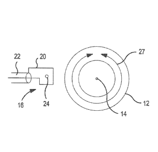
conventional
coil with "polarization " current of electrons in the dielectric material. The
polarization
current is due to the minor displacement of elementary charges bound to
molecules of the
dielectric material under the influence of an electric field. Both types of
current
(conduction current and polarization current) produce a magnetic field and an
induced
electric field according to the same laws of electromagnetism. However, since
the
dielectric material is at once its own capacitor and an inductor, the electric-
potential is
exactly zero everywhere inside the dielectric and in the space around the
dielectric.
Parasitic capacitive coupling is therefore entirely eliminated and the
electric field is
produced solely by induction. it is further believed that improved current
distribution is
obtained through lack of "skin" effects in the dielectric material that cause
conductive
current flow, unlike polarization current, to concentrate in the outermost
portions of a
ring structure.
[0009] Specifically then, the present invention provides a plasma generator
having a.
dielectric resonator structure having a central axis and a radiofrequency
power source
electrically coupled to the dielectric resonator structure to promote an
alternating
polarization current .flow at ,a natural resonant frequency of the dielectric
resonator
structure about the axis to generate plasma in an adjacent gas..
[0010] It is thus a feature of at least one embodiment of the invention to
provide an
improved radiofrequency antenna for the generation of intense but uniform
electrical
1
CA 02905929 2015-09-11
WO 2014/159588
PCT/US2014/024306
fields for plasma production.
[0011] The dielectric resonator may have any one or more of the qualities
of a
quality factor of greater than 100, an electrical resistivity greater than Ix
Q. cm, a
dielectric constant with a loss tangent of less than 0,01, and a dielectric
constant greater
than five,
[0012] It is thus a feature of at least one embodiment of the invention to
provide a
dielectric material that produces extremely low losses at radiofrequency
fields and high
power levels to minimize problems of cooling and energy loss.
[0013] The dielectric resonator may be of a material having melting point
greater
than a melting point of copper.
[0014] It is thus a feature of at least one embodiment of the invention to
provide a
material that is robust against the extremely high temperatures of plasma.
[0015] The dielectric material may, for example, be alumina (A1203) or
calcium
titanate (caTiO3),
[0016] It is thus a feature of at least one embodiment of the invention to
provide an
apparatus that may be constructed of relatively common and manufacturable
materials.
[0017] The dielectric resonator may be a ring having a central opening
along the axis.
[0018] it is thus a feature of at least one embodiment of the invention to
provide a
dielectric resonator that is relatively simple to manufacture,
[001.9] The ring may have a central opening of at least one millimeter
diameter or at
least one half inch.
[0020] It is thus a feature of at least one embodiment of the invention to
provide a
dielectric resonator that is readily adaptable to forming plasma in flowing
gas.
[0021] To that end, the plasma generator may include a gas port introducing
gas into
the ring along an axis of the ring.
[0022] It is thus a feature of at least one embodiment of the invention to
provide the
elements of a plasma torch for spectroscopic or other applications.
[0023] The radiofrequency power source may automatically seek the natural
resonant
frequency of the dielectric resonator structure to output radiofrequeney power
at the
natural resonant frequency of the dielectric resonator structure.
CA 02905929 2015-09-11
WO 2014/159588
PCT/US2014/024306
[0024] it is thus a feature of at least one embodiment of the invention to
provide a
plasma generator that may automatically adjust to variations in the dielectric
resonant
material or its environment.
[002.5] The radiofrequency power source may be a magnetron or a solid-state
or
vacuum tube oscillator.
[0026] It is thus a feature of at least one embodiment of the invention to
permit the
generation of extremely high frequency plasma.
[0027] These particular objects and advantages may apply to only some
embodiments
falling within the claims and thus do not define the scope of the invention.
BRIEF DESCRIPTION OF THE DRAWINGS
[0028] Fig. 1 is a partial cutaway perspective view of a plasma generator
using. a
ring dielectric resonator of one embodiment of the present invention;
[0029] Fig. 2 is a top plan view of the ring dielectric resonator of .Fig.
1 showing the
orientation of polarization current flow;
[0030] Fig. 3 is a model showing the electrical field in the ring
dielectric resonator of
Fig. 2;
[0031] Fig. 4 is a perspective view of an alternative embodiment of a ring
dielectric
resonator having standoffs for thermal conduction path to a supporting
structure and
airflow;
[0032] Fig. 5 is a perspective view of a ring dielectric resonator
fabricated of
individual sectors and showing one such sector;
[0033] Fig. 6 is a perspective view of a dielectric resonator fabricated
from multiple
laminated rings;
[0034] Fig. 7 is a perspective partial cutaway view of a dielectric
resonator fabricated
from a rod having circumferential 1,u-ooves and a central axial bore;.
[0035] fig. 8 is a perspective partial cutaway view of a disk dielectric
resonator
showing an external plasma region
[0036]. Fig. 9 is a perspective partial. cutaway view of a disk dielectric
resonator
providing a stepped surface disk to produce an axial disk-shaped plasma;
4
CA 02905929 2015-09-11
WO 2014/159588
PCT/US2014/024306
[0037] Fig. 10 is a perspective partial cutawayView of a nozzle for use in
plasma
cutting and welding or plasma thrusters;
[0038] Fig 11 is a fragmentary view of a loop power coupling system similar
to that
shown in Fig. 1 for inductively coupling electrical power into the dielectric
resonator;
[0039] Fig. 12 is a figure similar to Fig. II showing a coupling system
employing a
microwaVeVaveguide;
[0040] Fig: 13 is a perspective view of two identical ring-shaped
dielectric resonators
movable with respect to each other .for tuning;
[0041] Fig. 14 is a 'figure similar to Fig. 13 showing alternative tuning
structure in
which one dielectric resonator may fit over the other dielectric resonator for
tuning;
[0042] Fig, 15 is a perspective partial cutaway view of a dielectric
resonator
together with an RF shield in direct contact with an outer surface of the
dielectric
resonator.
[0043] Fig. 16 is a perspective partial cutaway view of a dielectric
resonator in
the form of two coaxial ceramic rings, together with two RE shields.
[0044] Fig. 17 is a simplified cross-sectional view of a spectrometer
incorporating the
dielectric resonator of the present invention;
[0045] Fig. 18 is a simplified, schematic cross-Sectional view of a mass
spectrometer incorporating the dielectric resonator of the present invention.
[0046] Fig. 19a and 19b are simplified cross-sectional views of compact
microwave
gas discharge lasers using the plasma system of the present invention ;
[0047] Fig. 20 is a simplified cross-sectional view of a diffusion cooled
coaxial
microwave gas discharge laser according to the present invention
[0048] Fig. 21 is a simplified cross-sectional view of aconveetion cooled
coaxial
microwave gas discharge laser according to the present invention
[0049] Fig. 22 is a simplified cross-sectional view of an electron-
cyclotron
resonance plasma source using the teachings of the present invention;
[0050] Fig. .23 is a simplified cross-sectional view of a large area, high-
density,
uniform plasma source according to the present invention;
[0051] Fig. 24 is a simplified cross-sectional view of a very large area,
high-
CA 02905929 2015-09-11
WO 2014/159588
PCT/US2014/024306
density, uniform plasma source according to the present invention;
[0052] Fig, 25 is a .simplified cross-sectional view of a microwave plasma
torch
using the present invention;
[0053] Fig. 26 is a simplified cross-sectional view of a microwave plasma
torch
such as may form the basis of a rocket engine;
[0054] Figs. 27a and 27b are top plan and side elevational cross-sectional
views
of an ion cyclotron resonance plasma heating system.
DETAILED DESCRIPTION OF THE PREFERRED EMBODIMENT
[0055] Referring now to .Fig. 1, a plasma generator 1.0 of the present
invention may
provide for a dielectric resonator 12 being in this embodiment a cylindrical
annulus
centered about an axis 14.
[0056] As is understood in the art, dielectric materials are substantially
insulators
with respect to direct currents (that is when a dielectric is placed in an
electric field
electrical charges do not now freely through the material as they do in a
conductor) but
can provide for polarization currents produced by slight shills in the
equilibrium positions
of bound electrons or ions in the material.
[0057] In this embodiment, the dielectric resonator 12 may be made of
alumina
(A1203) and may be a circular annulus or ring being two inches in outer
diameter, one
inch in inner diameter and 0.75 inches in length along axis 14 and having an
electrical
resonance at approximately 2.45 gigahertz. This material exhibits a quality
factor of
greater than 5000, a relative dielectric constant of 9.8 and retains its
electrical properties
and physical integrity at temperatures exceeding 1000 degrees centigrade.
[0058] An alternative material for the dielectric resonator 12 may be
calcium titanate
(CaTiO3) being 3.13 inches in outer diameter 2,34 'inches in inner diameter
and 1,12.
inches in length and resonating: at approximately 430 megahertz. This ring
exhibits a
quality factor in excess of 5000 and has a relative dielectric constant of
200.
[0059] Many types of advanced technical ceramics meet these requirements,
but
other dielectric materials with similar electrical properties may be used
instead.
[0060] More generally, the dielectric material of the dielectric resonator
12 may have
CA 02905929 2015-09-11
WO 2014/159588
PCT/US2014/024306
the following properties; (a) loss tangent less than 0.01, (b) quality factor
greater than
100, (c) relative dielectric constant larger than 5. Alternatively the quality
factor Should
be greater than 1000.
[0061] Desirably the dielectric material may have a resistivity greater
than 1x10¹⁰
ohm centimeters and typically greater than lx.1014 ohm centimeters. Desirably,
the
dielectric material may have aThelting point higher than copper or other
comparable
conductive metals.. The dielectric constant is preferably greater than five
and more
desirably greater than nine. These.examples are not intended to be limiting.
[0062] The resonant frequency of a rim, is approximately inversely
proportional to
the square root of the relative dielectric constant and approximately
inversely
proportional to the linear size of the ring, if all three dimensions of the
ring are changed
by the same factor, allowing these examples to be readily modified to other
dimensions.
[0063] The dielectric resonator 12 may be positioned near a coupling
antenna 16 in
turn attached to a radio frequency power supply 18 the latter producing a high
frequency
electrical current exciting the coupling antenna 16 at the resonant frequency
of the
dielectric resonator 12. Matching of the frequency output of the
radiofrequency power
supply 18 to the resonant frequency of the dielectric resonator 12 may be done
manually
by adjusting a frequency setting, or automatically, for example, by using a
feedback
System detecting impedance changes associated with resonance. Automatic tuning
may
also be provided by "self resonance" using feedback from a sensing antenna 19
whose
output drives the radiofrequency power supply 18 acting as an amplifier. Self
resonance
is provided by ensuring .a necessary loop phase shift as is generally
understood in the art.
The radiofrequeneypower supply 18 receives electrical power 21, for example,
line
current from a conventional source..
[0064] The
radiofrequency power source may be electrically coupled to the dielectric
resonator. As a magnetic field is also present, the radiofrequency power
source can be
both electrically coupled and magnetically coupled to dielectric resonator
structure; hence
the radiofrequency power source may be said to be electromagnetically coupled
to the
dielectric resonator structure. The coupling promotes an alternating
polarization current
flow at a natural resonant frequency of the dielectric resonator structure.
Generally, the
7
CA 02905929 2015-09-11
WO 2014/159588
PCT/US2014/024306
radiofrequency power source is driven at a frequency Or a range of frequencies
(such as
broadband) which is sufficient to couple at least some power into the
dielectric resonator.
structure at its natural resonant frequency. Preferably the radiofrequeney
power source is
driven at a frequency which is related to the natural resonant -frequency of
the dielectric
resonator structure. More preferably the radiofrequeney power source is driven
at a
frequency which is within two full width at half maximum (FWEIM) bandwidths of
the
resonant frequency of the dielectric resonator structure when the resonator is
loaded. The
bandwidth of an unloaded dielectric resonator is very narrow and may broaden
by a
factor of 100 when loaded with the plasma.
[0065] Referring now to Figs. 1 and 14, the resonant frequency of the
dielectric
resonator 12 may be adjusted not only by changing the dimensions of the
dielectric
resonator 12 but by placing a second dielectric tuning element 44 in proximity
to the
dielectric resonator 12. In this example of Fig. 1.4, the tuning element 44 is
a cylindrical
annulus larger than the outer diameter of the dielectric resonator 12 and
aligned with axis.
14. The tuning element 44 is attached to a mechanism 46 (for example, alaek
and pinion
lead. screw or the like) allowing it to be moved along the axis as indicated
by movement
arrow 50 to change the inductive coupling between tuning element 44 and
dielectric
resonator 12 thereby changing the resonant frequency of dielectric resonator
12. Because
tuning element 44 .may fit around dielectric resonator 12 close coupling may
be
established for sensitive tuning. The movement of the tuning elements 44 may
be manual
or automatic according to feedback control, for example, according to sense
impedance
as described above.
[0066] Referring now to .Fig. 1.3, in an alternative embodiment, two
identical
dielectric resonators 12a and 12b may be used with dielectric resonator 12b
acting as
tuning element 44. The use of two identical components provides greatly
increased
tuning range and an extended region of uniform electrical field. One or both
of the
dielectric resonator 12a and dielectric resonator 12b may provide for
electrical fields
generating plasma.
[0067]
Alternatively; in either of the above examples, the tuning elements 44 may he
a metal such as aluminum, copper, or silverplated copper to provide similar
tuning
8
CA 02905929 2015-09-11
WO 2014/159588
PCT/US2014/024306
effects.
[0068] Referring also to Figs. 2 and 11, in this example, the coupling
antenna 16 may
be a single loop 20 terminating a coaxial cable 22 leading to the power supply
18 and
having an axis 24 generally .parallel to axis 14 to couple electrical power
inductively
between the loop 20 and the dielectric resonator 12 with magnetic flux lines
26. The
single loop 20 may be adjusted as indicated by rotation an-ow 43 to control
the degree of
coupling and to provide proper alignment with axis 14. The result is a
polarization
current flow 27 within the dielectric resonator 12 (shown in Fig. 2).
oscillating
.circumferentially about axis 14 at the resonant frequency of the dielectric
resonator 12.
[0069] Referring now to Fig. 3, the electric field 28 within the dielectric
resonator 12
at a given instant in time is substantially tangential to the inner and outer
circumferential
peripheries of the dielectric resonator 12 representing a purely inductive
field where
parasitic capacitive coupling has been substantially eliminated. The electric
field .28 is.
believed to be of such a high quality because the dielectric resonator is at
once its own
capacitor and an inductor and therefore electric-potential is exactly zero
everywhere
inside the dielectric resonator 12 and in the space around the dielectric
resonator 12.
[0070] Referring again to Fig. 1, a gas source 32, for example, argon for
an argon-
based plasma may be provided through a regulator 34 to a gas port 36 directing
gas along
axis 14 through the center of the dielectric resonator 12. Within the
dielectric resonator
12, the high electrical fields convert the gas to a plasma 40 that may flow
along axis 14.
The distance of flow is determined by the lifetime of the plasma excitation.
The
dielectric resonator 12 may be placed in a radiofrequency shield 42 to reduce
power loss
due to radiation of electromagnetic energy, minimize human exposure to high
intensity
non-ionizing radiation and control electromagnetic interference. The shield 42
may be
connected_ to the return of the coaxial cable 22.
[0071] The use of
the dielectric resonator 12 instead of a conductive metallic multi or
single loop coil. directly driven by an amplifier provides multiple benefits
including:
a) Energy losses in the dielectric resonator 12 are one to two orders
of
magnitude lower than the conduction losses in a conventional coil. In many
applications,
this may completely eliminate the need for fluid cooling, greatly reducing the
size, .cost,.
9
CA 02905929 2015-09-11
WO 2014/159588
PCT/US2014/024306
and complexity of the plasma source. In semiconductor processing applications,
it may
be possible to eliminate the need for environmentally damaging dielectric
cooling fluids.
b) The extremely low energy losses in the dielectric resonator 12
translate
into a very large electric field strength during the plasma ignition phase,
when no power
is absorbed by the plasma. This makes for easier and more reliable ignition of
the plasma
discharge.
The self-resonant nature of a dielectric resonator 12 greatly simplifies or.
eliminates the need for an external impedance matching network between the
dielectric
resonator 12 and the power supply 1.8, thus reducing the size, cost, and the
complexity of
the plasma source.
d) The use of ceramic materials, .sach as alumina, in the dielectric
resonator
12 provides a plasma generator compatible with ultra-high-vacuum processes
that can be
placed directly inside a vacuum chamber in order to improve the coupling to
the plasma
or to accommodate limited space available for the plasma source.
Creating the dielectric resonator 12 from ceramic materials, such as
alumina which have high thermal conductivity, allows for rapid heat removal by
conduction. If the dielectric resonator 12 is in direct contact with plasma,
this can enable
an efficient codling of the plasma gas, a partioularlyimportant feature in gas-
discharge.
laser applications.
0 The use of ceramic materials, such as alumina for the dielectric
resonator
maintains good mechanical and electric characteristics at extremely high
temperatures in
excess of I ;000 degrees Centigrade, which makes a dielectric resonator 12
well suited to
applications involving high-temperature atmospheric plasma.
Pure inductive field, extremely low losses, high-temperature operation,
and high thermal conductivity, possible with the present design, all enable
operation at
power levels well in excess of what is possible today with the conventional
inductively
coupled plasma technology.
[0072] Referring
now to Fig. 4, in an alternative configuration dielectric resonator 12.
may provide for radially extending standoffs:52 that may, for example, support
the
dielectric resonator 12 against a supporting structure such as a tubular
shield 42 shown in
Fig. 1. The ends of the standoffs 54 may be plated with a metal in order to
reduce
CA 02905929 2015-09-11
WO 2014/159588
PCT/US2014/024306
thermal resistance to a metal enclosure to assist in cooling of the dielectric
resonator 12
which may also be cooled by natural convection or forced flow of air around
the
standoffs 52,
[0073] Referring now to Fig. 5, particularly for larger dielectric
resonators 12, the
dielectric resonator 12 may be assembled from multiple annular sectors 58
placed
together at seams 60 being an abutment of metal plated end surfaces 62. The
small
amount of non-dielectric material does not significantly impact the benefits
of the
dielectric.
[0074] Referring now to Fig. 6, the dielectric resonator 12 may be
constructed out of
multiple thin rings 64 aligned along common axis 14 held apart by thin
insulating spacers
66. Smaller rings may be easier to manufacture and transport and the gaps
between the
end surfaces. 62 may provide improved cooling while preventing undesirable
flow of
dielectric polarization currents in the axial direction.
[0075] Referring now to Fig 7, a similar result may be achieved by
fabricating the
dielectric resonator 12 in the form of an elongated tube 68 having a central
axial bore 70
and outer circumferential notches. 72 serving to prevent axial polarization
currents.
[0076] Referring now to Fig. 8, it will be appreciated that the dielectric
resonator 12
need not be a. ring but that a. toroidal plasma 40 may be generated around the
outer
periphery of a dielectric, resonator 12 in the form of a disk 74. The toroid
of the plasma
40 may be centered about axis 14 being an axis of symmetry of the disk 74.
Proper
selection of the resonant mode ensures a primary circumferential current
component in
the resonance of the disk 74.
[0077] Referring now to Fig. 9, by establishing a series of circular steps
76 of
increasing height as one moves toward the center of the disk 74, the plasma 40
may be
displaced to an opposite face of the disk 74 of the dielectric resonator 12.
The idea
behind the steps 76 is to address the tact that in a. simple ring or disk, the
electric field is
zero on the axis and increases nearly linearly towards the outer radius. The
field and the
plasma are most intense near the ring. The steps serve to increase the
polarization current
at smaller radii (by increasing the thickness) so that the induced electric
field is more
.uniform between the axis and the outer radius. It is believed that this may
improve radial
11
CA 02905929 2015-09-11
WO 2014/159588
PCT/US2014/024306
plasma uniformity. As far as displacing the plasma is concerned, plasma on the
other
side of the disk would have to be suppressed by high-vacuum or higher gas
pressure, for
example.
[0078] Referring now to Fig, 10, in one embodiment the dielectric resonator
12 may
provide for a convergent-divergent nozzle for the purpose of accelerating hot
subsonic
plasma flow 80 into supersonic plasma flow 82, in applications such as plasma
cutting
and welding or rocket engines. In this case, the dielectric resonator 12
includes .a central
bore 70 that neck inward to a smaller diameter 84, for example, to produce a
de .Laval
nozzle at a point of plasma generation.
[0079] It will be appreciated that that many variants shown in .the above
Figs. may be
combined in various ways. For example, the standoffs 52 of Fig. 4 can he
combined with
the rocket nozzle of Fig. 10 in order to facilitate heat removal, or the
notches 72 shown in
Fig. 7 can be implemented in the disks of Figs. 8 and 9, in the form of
circumferential.
grooves cut downward into one of the faces of the disk 74 to promote the
desired current
floW patterns.
[0080] Referring now to Fig. 12, other methods of exciting the dielectric
resonator 12
into resonance may be employed, for example, placing the dielectric resonator
12 at the
end of a waveguide 89 directed generally perpendicular to the axis -14 driven
by a
microwave source. An opening 90 of the waveguide 89 may be controlled by an
iris
mechanism that may open and close iris 94 as indicated by arrows.-92 to
control the
degree of coupling between the microwave source and the dielectric resonator
12
[0081] Referring now to Fig. 15, the .RF shield 42 may be in direet.Contact
with
an outer surface of the dielectric resonator 12. This configuration offers the
advantage of smaller size and better transfer of heat to the RF shield 42. The
surface
of the ceramic ring 12 which is in contact with the RI' shield 42 may be
plated with
metal.
[0082] Referring now to Fig. 16, plasma 40 may be formed in the annular gap
between two concentric ceramic rings 1-2c and 12d. The outer surface of the
larger
ring 12c is in direct contact with outer RF shield 42a. The inner surface of
the
smaller ring 12d is in direct contact with inner RF shield 42b. The annular
gap
12
CA 02905929 2015-09-11
WO 2014/159588
PCT/US2014/024306
between concentric rings 12e and 1.2d is preferably located at or near the
radius
where the electric field strength is the highest.
Example 1 Optical Emission Spectroscopy
[0083] The present invention may be used in an optical emission
spectrometer (OES)
where their purpose is to excite the atomic and molecular species in an
unknown
chemical sample and produce light. The spectroscopic analysis of the light
emitted by
the plasma is used to determine the type and quantity of the chemical
substance present in
the sample. Plasma properties critically affect the analytical performance of
an OES, in
terms of the ability to process samples in aqueous or organic solvents without
extinguishing the plasniaõ the ability to operate on different plasma gases
for unproved
safety and economy, the ability to detect different kinds of chemicals, the
ability to
accurately measure a very large range of andlyte concentrations, the ability
to detect
extremely small concentrations of the analyte, the ability to process many
samples in a
short amount of time, the ability to produce stable results when measurements
are
repeated over a long period of time, etc.
[0084] Typical plasma sources for this application may operate at radio-
frequencies
up above 40 MI-Iz with much higher frequencies implemented by this design.
Alternatively, the design may provide plasma at microwave frequencies, such as
915
Wiz or 2,450 MHz, using a magnetron device as a source of large amount of
microwave
power. Existing designs for plasma generators are dominated by capacitive
coupling or
retain a significant amount of parasitic capacitive coupling, which has a
serious negative
impact on the plasma source, or have form factors that would require
significant
modifications to the conventional mechanical, optical, and chemical interface
to the rest
of the spectrometer, an interface which has proven itself over many years of
operation of
radio-frequency OES in the field.
[0085] In contrast, the plasma..source of the present design may extend the
operation
of the conventional radio-frequency inductively coupled plasma sources to
microwave
frequencies, practically eliminating parasitic capacitive coupling which has
limited.
previous designs, while requiring minimum modifications to the established
mechanical,
13
CA 02905929 2015-09-11
WO 2014/159588 PCT/US2014/024306
optical, and chemical interface with the rest of the spectrometer. In
addition, the
extremely low losses of the novel field applicator, allow for a complete
elimination of the
fluid cooling system, thus reducing the size, cost, and the complexity of the
spectrometer.
[0086] Referring now to Fig. 17 a microwave inductively coupled plasma
source for
optical-emission spectroscopy 102 .uses a dielectric resonator 12 of the
present invention,
made out of high-density Alumina (Al2O3) ceramics in the form of a circular
annulus,
The dielectric resonator 12 may be supported within cylindrical radio-
frequency shield 42
made of metal, such as alumin.um, and has several circular openings 104, 106,
and 108
each surrounded with aluminum tubular extensions 110, 112, and 114
respectively. The
tubular extensions 110-114, are designed to have a sufficiently small diameter
and
sufficiently long length to form cylindrical waveguides below cutoff, greatly
attenuating
the propagation of microwaves through the extension tubes, as is well
understood in the
microwave art, in order to minimize the leakage of microwave energy outside of
the
shield 42.
[0087] Microwave power 118 from waveguide 89 communicating with magnetron
.120 is provided at a frequency of 2,450 MHz and applied to the dielectric
resonator 12
dint a rectangular opening 90 in the shield 42 by the means of a coupler 124.
The
resonant frequency of the dielectric resonator 12 can be finely adjusted by
varying the
axial location of the tuning element 44, made in the form of an aluminum ring,
positioned
coaxially with the ring of dielectric resonator 12.
[0088] A triaxial manifold 125 is directed along the axis 14 centered
within opening
104 and aligned with inner diameter of dielectric resonator 12 and made out of
quartz or
alumina tubing. A. plasma cooling gas 126 is applied to an outer ring of the
triaxial
manifold 125 while a plasma auxiliary gas 128 is applied to the next inner
ring and the
center bore receives the dissolved analytical sample 130 from a sample source
132 being
analyzed. The sample 130 is in the form of an aerosol that may be directly
introduced
into the plasma 40.
[0089] Light 134 emitted from the plasma 40 in a direction radial to axis
14 passes
through the tubular extension 112 for analysis by a. light sensor 136 coupled
to an
analyzing computer 138 that may determine frequency components of the light
134
14
CA 02905929 2015-09-11
WO 2014/159588
PCT/US2014/024306
according to methods known in the art. Alternatively or in parallel, for the
purposes of
the, so called, axial OES, light 140, emitted by the plasma 40 in the axial
direction of axis
14, is transferred through the tubular extension 110 for further spectroscopic
analysis by a.
similar light sensor 136 (not shown for clarity). The tubular extension 110
also directs
the hot plasma gases and chemical products 142 to an exhaust venting system
(not
shown.) The opening 108 and the tubular extension 114 allow for air cooling of
the
plasma generator 12 by natural convection or by forced flow of air.
Example 2 Mass Spectroscopy
[0090] The present invention offers similar advantages in both optical
emission and
mass spectroscopy (MS)õ with the added advantage in mass spectroscopic
applications of
an improved control over ion velocities, increased ion collection efficiency,
and reduced
.sputtering of the sampler cone.
[0091] Referring now to Fig. 18, a microwave inductively coupled plasma
source for
mass spectrometry 200 uses a field applicator 12 of the present invention,
made of high-
density Alumina (A1203) ceramic in the form of a ring. The microwave
inductively
coupled plasma source for MS 200 has many components in common with the
microwave inductively coupled plasma source for OES 102 shown in Fig. 17,. and
like
components have the same identifiers. Additional components shown in Fig. 18
will now
be described. The sampler cone 201 has a small orifice 202 and the skimmer
cone 203
has a small orifice 204. The region between the sample cone 201 and the
skimmer cone
203 is maintained at a low pressure by exhausting the gas 205 by means of a
vacuum
pump (not shown). The ionized sample 206 enters the low pressure region
between the
sample and skimmer cones through the orifice 202. tons 207 are firther
transmitted
through the orifice 204 into the high-vacuum region of the mass-spectrometer.
The mass
spectrometer comprises ion focusing components .209 which comprise at least
one ion.
focusing element, a mass analyser 210 and an ion detector 211. There may be
two or
more stages of pumping (not shown) disposed within the mass spectrometer. The
mass
spectrometer is controlled by a controller (not shown), which is preferably a
computer.
Detected signal from ion detector 211 is recorded, preferably also
using:a.computer,
CA 02905929 2015-09-11
WO 2014/159588
PCT/US2014/024306
which may be the same computer as is used as the controller. The heated plasma
gas 208
which has not penetrated the orifice 202 is exhausted through the annular
region between
the RF shield 42 and the sample cone 201.
Example 3 -Convection Cooled Microwave Gas Discharge Laser
[0092] A plasma generator of the present invention may be used to construct
a
compact, medium-power, gas-discharge laser producing a high-quality beam of
several
hundred Watts of optical power. The design is based on convection cooling and
pure
inductively coupled gas-discharge at a microwave .frequency.
[0093] Figs. .19a and 19b show a cross-section and a top view,
respectively, of a
medium power compact gas-discharge laser 300 based on the dielectric resonator
1.2 of
the present invention. The dielectric resonator 12 is in the form of an
elongated tube 68
with axis 14, having a central axial bore 70 and outer circumferential notches
72 (see Fig.
7.) Dielectric resonator 12 may be made of high density Alumina (A1203). A
cylindrical
RF shield 42 includes a plasma gas inlet 302 and a plasma gas outlet 304. Cold
:gas 306
enters through the gas inlet 302, flows through the central axial bore 70,
arid exits as
heated gas 308 through the gas outlet 304. inlet 302 and outlet 304 are
connected to a
gas circulation system (not shown) which includes a. blower and a heat
exchanger for
cooling the gaS,. as is wellknoWn.in the art. Microwave power 118, such as
.provided by
a 2,450MHz magnetron (not shown), is coupled to the laser 300 by means of a
waveguide
port 124 in the RF shield 42 which has an opening 90 defined by a pair of
irises 94. An
inductively coupled plasma 40 is formed in the inner bore 70 of the dielectric
resonator
12. Flat ends of the cylindrical shield 42 support a reflective spherical
mirror 310 and a
semi-transparent spherical mirror 312 which form an optical cavity. Plasma 40
is an
optical gain medium inside the optical cavity formed by. mirrors 310 and 312
and results
in the emission of a high-quality axially symmetrical optical beam 314 of
several hundred
Watts which can be focused at a spot of very small size by suitable external
optical
components (not shown). The surfaces of the dielectric resonator 12 which are
in contact
with the metal shield 42 are preferably metal plated.
Example 4 -Diffusion. Cooled Coaxial Microwave Gas Discharge Laser
16
CA 02905929 2015-09-11
WO 2014/159588
PCT/US2014/024306
[0094] A plasma
generator of the present invention may be used to construct a high-
power gas-discharge laser of scalable design, capable of producing high
.quality optical
beam with an optical power of several kilowatts. The optical design adopts a
coaxial,
diffusion-cooled configuration which is well known in the art. Diffusion
lasers do not
require a blower and consume minimal amount of gas. However, while the plasma
in a
conventional coaxial. laser is sustained by a pure capacitive RF discharge
between inner
and outer coaxial electrodes, which sets a power limit due to discharge
instabilities
inherent in capacitivecoupled plasma, the present invention .usesan
inductively coupled
plasma to obtain a stable discharge at higher power level while at the same
time operating
at a microwave frequency where high power magnetrons can be used .as more
convenient,
compact, and efficient power sources. hi addition, due to the high thei mai
conductivity of
the ceramic field applicator which is in direct contact with the laser gas,
the effectiveness
of the diffusion cooling is preserved.
[0095] Fig. 20 shows a cross-section of a high-power diffusion-cooled
coaxial laser
400 using a dielectric resonator of the present invention in the form of
ceramic rings 12c
and 12d. A cylindrical RF shield consists of a larger diameter metal tube 42a
and a
smaller diameter metal tube 42b with a common axis 14. The space between the
tubes
42a and 42b is hermetically sealed by flat end-plates 42e and 42d and filled
with a lasing
gas, such as a mixture of carbon-dioxide (CO2), nitrogen (N2), and helium
(He). A
reflective tonic mirror 402 and a semi-transparent tonic. mirror 404 are
mounted on .plates
42d and 42c9 respectively, and form a coaxial optical cavity. The inner RP
shield 42b is
surrounded by avaten jacket 406 which includes a water inlet 408 and a water
outlet 410.
Cold water 412 enters the inlet 408 and the heated water 414 is removed
through the
water outlet 410. The outer RF shield 4.2a is surrounded by a water jacket 416
which.
includes water inlet 418 and a water outlet 420. Cold water 422 enters the
inlet 418 and
the heated water 424 is removed through the outlet 420. Parts shown between
sections
AA' and BB' form a modular assembly that can be repeated in the axial
direction 14 one
or more times to increase the output beam power of the laser. One of 3 such
identical
modules shown in Fig. 18 will now be described. Outer RF shield 4.2a also
includes
wa.veguide pons 124 with openings 90 defined by pairs of irises 94. Microwave
power
17
CA 02905929 2015-09-11
WO 2014/159588
PCT/US2014/024306
i 18 can be supplied to each of the WaVeguide ports 124 by a separate
microwave.source
(not shown), such as from high-power 915MHz or 2,450MHz magnetrons normally
used
for industrial heating applications. Dielectric resonator consists of two
rings, the outer
ring 12c and the inner ring 12d, made from a ceramic material such as high
density
Alumina (A1203). The gap between the outer surface of the inner ring 12d. and
the inner
surface of the outer ring 12c is only a few millimeters wide in order to
enable an effective
transfer of heat by thermal diffusion from the gas to the ceramic rings 12c
and 12d. High
thermal conductivity of the ceramic rings rapidly transfers the heat from the
plasma gas
to the water flowing inside the cooling jackets 406 and 416. Plasma 40,
sustained by a
pure inductive coupling, forms an optical gain medium inside the optical
cavity formed
by tone mirrors 402 and 404. This results in the emission of a high-power,
cylindrically
symmetric, 'high quality coaxial optical beam 426 which, as is well known in
the art, can
be focused by external optical components (not shown) to a spot of small size.
Metal
rings 428 and 430 serve to minimize the inductive coupling between the modules
and to
facilitate the diffusive transfer of heat from the gas to the water flowing
inside the
cooling jackets 406 and 416. If the thickness of the ring is defined as the
difference
between. the outer and the inner radius of the ring, Fig. 20 shows both rings
12c and 12d
as having approximately identical thickness. However, the present invention is
not
limited to rings of equal thickness..
Example 5 ¨Convection Cooled Coaxial Microwave Gas Discharge Laser
[0096] A plasma generator of the present invention may be used to construct
a very-
high-power gas-discharge laser of scalable design, capable of producing high
quality
optical beam with a power of tens of kilowatts. The design adopts a coaxial,
convection-
cooled configuration which is well known in the art. However, while the plasma
in a
conventional coaxial laser is sustained by a pre capacitive RF discharge
between inner
and outer coaxial electrodes, which sets a pOW-er limit due to discharge
instabilities
inherent in capacitive coupled plasma, the present invention uses an
inductively coupled
plasma to obtain a stable discharge at higher power level while at the same
time operating
at a microwave frequency where high power magnetrons can be used as more
convenient,
18
CA 02905929 2015-09-11
WO 2014/159588
PCT/US2014/024306
compact, and efficient power sources.
[0097] Fig. 21 shows a cross section of a convection cooled inductively
coupled
coaxial gas discharge laser 500 using a dielectric resonator of the present
invention in the
form of ceramic rings 12e and 12d, The RF Shield is formed by an outer
metallic tube
42a and an inner metallic tube 42b with a common axis 14. The space between
the tubes
42a and 42b is hermetically closed with flat plates 42c and 42d, which support
a
reflective tonic mirror 402 and a semi-transparent tone mirror 404. Mirrors
402 and 404
form atoaxial optical cavity, as 'is well known in the art of high power gas
discharge
lasers. Parts shown between sections AA' and BB' form a modular assembly that
can be
repeated in the axial direction 14 one or more times to increase the output
beam power of
the laser. One of 3 such identical modules shown in Fig. 19 will now be
described. The
outer IRF shield 42a is .provided with gas. inlets 302 and outlets 304. Cold
plasma gas 306
enters the laser 500 through the inlet 302 and the heated plasma gas 308
leaves through
the outlet 304. Inlets 302 and outlets 304 are connected to a gas circulation
system (not
shown) which includes a very high flow-rate blower and a heat exchange system
for
cooling the gas, as is well known in the art. The direction of the gas flow is
indicated by
arrows 502. The outer RF Shield 42a also includes waveguide ports 124 with
openings
90 defined by pairs of irises 94. Microwave power 118 can be supplied to each
of the
ports 124 by a separate microwave source (not shown), such as from high-power
915MHz magnetrons normally used for industrial microwave heating applications.
Dielectric resonator consists of two rings, the outer ring 12c .and the inner
ring 12d, made
from a ceramic material such as high density Alumina (A1203), The gap between
the
outer surface of the inner ring 12d and the inner surface of the outer ring
.12c is
approximately 1 to 2cm wide to provide sufficient cross-sectional area for the
high flow-
rate of the plasma gas for heat removal purposes. Plasma 40, sustained by pure
inductive
coupling, forms an optical gain medium inside the optical cavity formed by
tonic mirrors
402 and 404. This results in the emission of a very high power, cylindrically
symmetric,
high quality onaxial optical beam 426 which, as is well known in the art, can
be focused
by external optical components (not shown) to a spot. of small size. Metal
rings 504 and
506 with a rounded edge have a three-fold purpose: to confine the
electromagnetic field
19
CA 02905929 2015-09-11
WO 2014/159588
PCT/US2014/024306
to the region occupied by the rings 12c and 1.2d, to minimize the inductive
coupling.
between adjacent modules, and to help guide the high-speed flow of plasma gas
306 and
308. The surfaces of the ceramic rings 12c and 12d which are in contact with
metal
shields 42a .and 42b and metal rings 504 and 506 are preferably metal plated.
If the
thickness of the ring is defined as the difference between. the outer and the
inner radius of
the ring, Fig. 21 shows both rings 12c and 12d as having approximately
identical
thickness. However, the present invention is not limited to rings of equal
thickness.
Example 6 ¨ Electron-Cyclotron-Resonance Plasma Source
[0098] A plasma generator of the present invention may be used to construct
an
electron-cyclotron-resonance plasma source. The source may be used for plasma
processing of semiconductor wafers, as an ion source, or as an ion-thruster
for in-space
propulsion.
[0099] Fig. 22 shows an electron-cyclotron-resonance plasma source 600
using a
dielectric resonator 12 of the present invention in the form of a ring.
Dielectric resonator
12 is made from an advanced technical ceramics material, such as calcium-
titanate
(CaTiO3) ceramics, having a large relative dielectric constant and very low
dielectric
losses. A cylindrical RE shield 42, made from a non-magnetic material, such as
stainless
steel, is surrounded by a set of electromagnets or permanent magnets 602 in
order to
create a static magnetic. field suitable for the production of electron-
cyclotron-resonance
(ECR) plasma, as is well known in the art of ECR. plasma sources. Radio-
frequency
power 150 is supplied through a coaxial transmission line 22 terminated by a
coupling
loop 20. One end of the coupling loop 20 is connected to the center conductor
of the
coaxial cable 22 and the other end of the loop is connected to the RE' shield
42. Quartz
tube 604 and RE Shield 42 form a gas tight enclosure such that the space
inside the quartz
tube 604 can be maintained at low pressure while the rest of the plasma source
is at
atmospheric pressure. Cold air or cooling fluid 606 removes the heat from the
field
applicator 12, quartz tube 604, and the RE shield 42, and is: eXhausted as
heated air or
fluid 608. Low pressure plasma gas 610 enters the quartz tube 604 where it is
converted.
to plasma 40. Plasma is sustained by the combined action of a pure inductive
RE field of
CA 02905929 2015-09-11
WO 2014/159588
PCT/US2014/024306
the field applicator 12 and the static magnetic field of the elect or
permanent magnets
602. Spent gas 612 is removed by the action of a vacuum pump (not shown)
connected
to the vacuum vessel 614. In ion-thrusters for in-space propulsion, the vessel
614 would
be replaced by a vacuum of interplanetary space. Ions 616 are extracted from
plasma 40
by a system of grid electrodes 618, held at various electrostatic potentials
by external DC
power supplies (not shown), as is well known in the art of ion sources.
[00100] The preceding description of the ECR plasma source 600 shown in Fig.
22
assumes an excitation 150 in the form of RF energy. However, the dielectric
resonator
12 of the present invention may be adopted for operation over a broad range of
frequencies. For example, by changing the material of the field applicator 12
to high-
density Alumina (A1203), the ECR plasma source of Fig. 22 could be made to
operate at
a microwave frequency, provided that the static magnetic field of
electromagnets 602 is
increased proportionally to the frequency. Optionally, for operation at
microwave
frequencies, coaxial cable 22 and the loop coupler 20 may be replaced by a
waveguide
and an iris coupler, respectively.
[00101] The primary function of the ECR plasma source 600 shown in Fig. 22 as
a
source of ions 616 has been chosen for illustrative purposes only. By removing
the grid
electrodes 618 and allowing a direct penetration of plasma 40 into the vacuum
vessel
614, it becomes possible to use the ECR plasma source 600 for many other
applications,
such as chemical-vapor-deposition, plasma etching, plasma ashing, vacuum ion
pumps,
etc.
[00102] In some applications it may be advantageous to operate the plasma
source 600
shown in Fig. 22 without electromagnets 602. Although in such a case there
will be no
enhancement of the plasma density by an ECR effect, the high efficiency and
pure
inductive coupling of the field applicator 12 of the present invention would
still enable
the production of high-density uniform plasma 40 superior to the conventional
RF
inductively coupled sources.
Example 7 - Large Area, High-Density, Uniform Plasma Source
[00103] A plasma generator of the present invention may be used to construct a
high-
21
CA 02905929 2015-09-11
WO 2014/159588
PCT/US2014/024306
density, uniform plasma source suitable for processing of semiconductor
wafers.
[00104] Fig. 23 shows a plasma source 700 using a dielectric resonator of the
present
invention made in the form of a:stack of one or more ceramic rings 64, held
apart by
spacers 66. Cylindrical RF shield 42 has a cooling water jacket 416. Cold
water 422
removes the heat from the RF shield 42 and heated water 424 carries it to the
chiller (not
shown) which is part of a closed cooling system. Since the cooling water comes
in
contact only with the grounded RF Shield 42, there is no need to use
environmentally
damaging dielectric cooling -fluids as would be required when cooling the coil
of a
conventional inductively coupled plasma source. The heat generated inside the
RP. shield
42 is conducted to the walls of the .RF shield by highly thermally conductive
ceramic
material of the dielectric resonator rings 64 whose outer cylindrical surface
is in direct
contact with the RF shield 4.2. RF power 150 is applied through a coaxial
transmission
line 22 terminated by a loop coupler 20 which is protected from the harsh
plasma
environment by a quartz or ceramic cap 704 which forms a gas tight fit with
the RF
shield 42. Low pressure plasma gas MO is excited to plasma 40 by the action of
the stack
of dielectric resonators 64 and spent gas 612 is removed by a turbo-molecular
vacuum
pump (not shown.) Plasma 40 facilitates plasma processing of a semiconductor
wafer
706 held on a chuck 708. The chuck 708 may contain an .RF bias electrode '710
supplied
by a coaxial transmission line 712 with RF power 714 which is generally at a
different
.frequency form the RF power 150 used to sustain the plasma.
Example 8 ¨ Very Large Area, High-Density, Uniform Plasma Source
[00105] A plasma generator of the present invention may be used to construct a
high-
density plasma source producing uniform plasma over a very large area,
suitable for
processing of large semiconductor wafers and solar panels.
[00106] Fig. 24 shows a plasma Source 800 using the dielectric resonator of
the present
invention in the form of a ceramic disk 74 with steps 76 of variable
thickness. The
thickness of steps 76 may be optimized to obtain a radial distribution of
dielectric
polarization currents inside the dielectric which results in the Most uniform
plasma 40.
Cylindrical RF shield 42 has a cooling water jacket 416. Cold water 422
removes the
22
CA 02905929 2015-09-11
WO 2014/159588
PCT/US2014/024306
heat from the RE shield 42 .and heated water 424 carries it to the chiller
(not shown)
which is part of a closed cooling system. The heat generated inside the RF
shield 42 is
conducted to the walls of the RE shield by highly thermally conductive ceramic
material
of the dielectric resonator 74 whose outer cylindrical surface is in direct
contact with the
RE shield 42. RF power 150 is applied through a coaxial transmission line 22
terminated
by a loop coupler 20. Plasma gas 610 is admitted to the space above the disk
74 and
flows through narrow capillary holes 802 evenly distributed across the surface
of the disk
74, creating a showerhead effect. Due to the pressure drop across the narrow
holes,
pressure above the disk 74 is sufficiently high such that no plasma forms in
this part of
the plasma source 800. Plasma gas 610 flowing out of the bottom of the disk 74
is.
:excited to a large-area, high-density, uniform plasma 40 and the spent gas 02
is removed
by a turbo-molecular vacuum pump (not shown.) Plasma 40 Facilitates plasma
processing of a large diameter semiconductor wafer or a solar panel 706 held
on a chuck
708. Chuck 708 may contain an RF bias electrode 710 supplied by a coaxial
transmission
line 712 With RE' power 714 which is generally at a different frequency form
the RF
power 150 used to sustain the plasma.
Example 9 ¨ Microwave Plasma Torch
[00107] A plasma .gencrator of the present inventioritiay be used to construct
electrode-less atmospheric plasma torches powered by inductively coupled
microwave
energy. Such torches may he used in advanced manufacturing, environmental,
chemical
synthesis, space, and scientific applications.
[00108] Fig, 25 shows an atmospheric microwave plasma torch 850 based on the
plasma source using dielectric resonator 12 of the present invention. A
cylindrical RF
shield 42 is surrounded by a water cooling jacket 416 with an inlet for cold
water 422 and.
outlet for heated water 424. Dielectric resonator 1.2 is made in the form of a
ceramic ring
whose outer cylindrical surface is in direct contact with the RF shield 42 for
efficient
removal of heat. .RF shield 42 also includes waveguide port 1:24 with opening
90 defined.
by a pair of irises 94. Microwave power 118 can be supplied to the waveguide
port 124
from a magnetron (not shown.) A triaxial manifold 852, made of Alumina
ceramics or
23
CA 02905929 2015-09-11
WO 2014/159588
PCT/US2014/024306
quartz, guides the cooling gas 854, the auxiliary gas 856, and the particles
of the material
to be sprayed 858, thru the center opening of the dielectric resonator ring
12. High-
temperature atmospheric pressure plasma 40 melts the material 858, creating a
spray of
molten material 860 which is implanted or deposited onto the surface of the
object 862
undergoing surface treatment. As is well known in the art of atmospheric
plasma torches,
plasma-spraying application shown in Fig. 23 is only one of many possible
applications
which may be realized by using different substances 858 and objects 862
undergoing
high-temperature plasma treatment.
[00109] Fig. 26 shows microwave plasma torch 870 based on a dielectric
resonator 12
with a central bore 70 that necks inward to a smaller diameter 84, to form a
convergent-
divergent nozzle 111. A cylindrical RF shield 42 is surrounded by a water
cooling jacket
416 with an inlet for cold water 422 and outlet for heated water 424. The
outer surface of
the dielectric resonator 12 is in a direct contact with the RF shield 42 for
an efficient
transfer of heat. RF shield 42 also includes waveguide port 124 with opening
90 defined
by a pair of irises 94. Microwave power 118 can be supplied to the waveguide
port 124
from a magnetron (not shown.) A biaxial manifold 872, made of Alumina or
quartz,
guides the cooling gas 854 and the plasma gas 874 into the central bore 70.
Plasma gas
874 is converted to plasma and heated to high temperature by the absorption of
microwave energy 118, thus forming a high-temperature subsonic flow 80. Large
thermal energy of the subsonic flow 80 is converted to the kinetic energy of
the
supersonic flow 82 by the action of a convergent-divergent nozzle 111.
Supersonic flow
82 can be used in advanced manufacturing applications, such as plasma welding
and
cutting, as well as in thermal rockets for in-space propulsion.
Example 10 ¨ Ion Cyclotron Resonance Plasma Heating
[001101 A plasma generator of the present invention may be used to construct
an ion-
cyclotron heating (ICRH) antenna for applications such as fusion reactors or
variable-
specific-impulse magnetoplasma rocket (VASIMR) for in-space propulsion.
[001111 Figs. 27a and 27b show cross-sections A-A and B-B, respectively of a
tokamak fusion reactor 900 using dielectric resonators 12 of the present
invention.
24
CA 02905929 2015-09-11
WO 2014/159588
PCT/US2014/024306
Vacuum vessel:42 also serves as an. RF shield and is surrounded by
superconducting
electromagnets 902 which create a toroidal static =magnetic field for the
magnetic
confinement of plasma 40. Dielectric resonator 12 is made in the form of a
ring, from a
dielectric ceramic material with a large relative dielectric constant. RF
power 150 of the
order of millions of Watts at a frequency betweentOMHz and 1001V1flz, typical
of ICRIL
is supplied through a coaxial transmission line 22 terminated by .a loop
coupler 20
located inside a cavity 904 which forms the part of the RI shield 42.
[00112] Certain terminology is used herein for purposes of reference only, and
thus is
not intended to be limiting. For example, terms such as "upper'', "lower",
"above", and
"below" refer to directions in the drawings to which reference is made. Terms
such as
"front", "hack", "rear", "bottom" and "side", describe the orientation of
portions of the
component within a consistent but arbitrary frame of reference which is made
clear by
reference to the text:and the associated drawings describing the component
under
discussion. Such terminology may include the words specifically mentioned
above,
derivatives thereof, and words of similar import. Similarly, the terms
"first", "second"
and other such numerical terms referring to structures do not imply a sequence
Or order
unless clearly indicated by the context.
[00113] When introducing elements or features of the present disclosure arid
the
exemplary embodiments, the articles "a", "an", "the" and "said" are intended
to mean that
there are one or more of such elements or features. The terms "comprising",
"including"
and "having" are intended to be inclusive and mean that there may be
additional elements
or features other than those specifically noted. It is further to be
.understood that the
method steps, processes, and operations described herein are not to be
construed as
necessarily requiring their performance in the particular .order discussed or
illustrated,
unless specifically identified as an order of performance. It is also to be
understood that
additional or alternative steps may be employed.
[00114] The term "ring" should be understood to generally mean a topological
surface
of genius one and not require nor exclude, for example, a circular profile,
radial
symmetry or particular aspect ratios of with a diameter to height except as
explicitly
noted.
[00115] It is specifically intended that the present invention not be limited
to the
embodiments and illustrations contained herein and the claims should be
understood to
include modified forms of those embodiments including portions of the
embodiments and
combinations of elements of different embodiments as come within the scope of
the
following claims.
26
Date Recue/Date Received 2020-04-09