Note: Descriptions are shown in the official language in which they were submitted.
MICROWAVE PLASMA SPECTROMETER USING DIELECTRIC
RESONATOR
[0001]
Field of the Invention
[0002] The present invention relates generally to electrical antennas and
in particular to
an antenna generating an efficient and uniform electromagnetic field for
plasma generation
and the like. The present invention is particularly directed to the generation
of plasma into
which is introduced a substance to be analysed, the plasma causing
atomization, excitation and
ionization of the substance so that the light it then emits or absorbs, or the
ions produced, may be
analysed to determine properties of the substance.
Background to the Invention
[0003] Plasma sources are used for the generation of gaseous plasma whose
unique physical,
chemical, optical, thermal, and biological effects are extensively used in
broad areas of science
and industry. High-frequency plasma sources utilize radio-frequency or
microwave electrical
energy to sustain a plasma. High-frequency plasma sources typically include a
radio- frequency
(RF) shield in order to minimize human exposure to high intensity non-ionizing
radiation and
reduce electromagnetic interference and power losses due to the radiation of
electromagnetic
energy. Although plasma is typically produced inside an RF shielded enclosure,
the beneficial
effects of plasma may be realized either inside or outside the radio-
frequency shield.
[0004] Plasma sources which use radio-frequency or microwave energy to
sustain plasma are
usually classified as belonging to one of two broad categories, capacitively
coupled or
inductively coupled. A capacitively coupled plasma source relies on electrical
charges stored on
capacitor plates to produce an electric field which accelerates the electrons
and ions in the
plasma. On the other hand, an inductively coupled plasma source relies on a
changing magnetic
field, produced by the current flowing through a coil, to induce an electric
field in the plasma as
described by the Faraday's law of induction. Both capacitively and inductively
coupled plasma
1
CA 2905931 2019-10-17
CA 02905931 2015-09-11
WO 2014/159590 PCT/US2014/024312
sources find extensive application in the processing of semiconductor wafers.
While the
capacitively coupled sources are suitable for producing a uniform low-pressure
plasma over a
relatively large area, inductively coupled sources are capable of producing
higher density plasma
within a smaller volume. In addition, inductive sources are more efficient in
coupling large
amounts of electrical power into highly electrically conductive plasma, such
as in atmospheric
plasma torches which generate very high temperature plasma at atmospheric
pressure with many
applications in science and industry. The present invention relates to
inductively coupled plasma
sources. High frequency electrical fields for the generation of plasma may
make use of a
conductive coil ("field applicator") driven by an AC current oscillating in
the MegaHertz to
GigaHertz range. A gas within the coil receives energy from the coil through
inductive coupling
exciting the gas into a plasma state.
[0005] Such inductive coupling techniques for generating plasma have a
number of
significant problems. First, normally the conductive coil must have multiple
"turns" and each
turn exhibits a mutual capacitance with adjacent turns of the loop creating
field (and hence
plasma) inhomogenieties which may be manifested as nonuniform plasma ion
speeds,
trajectories and densities.
[00061 Nonuniformities in the plasma may adversely affect applications in
which a uniform
plasma is required (for example, for etching in the integrated circuit
industry) and may waste
energy on undesired plasma processes. Since the regions of plasma with higher
electron density
absorb more power than the regions with lower electron density, the ionization
is further
enhanced in high density regions and reduced in low density regions, which may
lead to
instability. The less uniform the electric field, the more likely it is that
the plasma will exhibit
instabilities ranging from a departure from a local thermodynamic equilibrium
to a contraction
into a filamentary discharge. Furthermore, a disproportional energy absorption
by the plasma in
the regions of high field intensity, which are usually located close to the
antenna. limits the
energy available to other regions of the plasma. The mutual capacitance also
limits the voltage
that may be applied to the conductive coil without dielectric breakdown
between the turns of the
coil.
[0007] Second, the large amount of electrical power and hence large amounts
of electrical
current required to pass through the conductive coil produce significant
resistive heating
2
CA 02905931 2015-09-11
WO 2014/159590 PCT/US2014/024312
requiring complicated or bulky cooling structures. The use of highly
conductive materials, such
as copper, can reduce resistive losses, but the use of copper and similar
metals is complicated by
the susceptibility of such highly conductive materials to corrosion and
melting in the harsh
envirorunent of the plasma.
[0008] Third, efficient driving of the conductive loop requires that the
loop be part of a
resonant .structure implemented by placing a tuning capacitor into the coil
circuit.
[0009] Capacitors suitable for this purpose are expensive and bulky, and
the tuning capacitor
may require automated control in order to match the differing load when
firstly igniting the
plasma and then after stable plasma has been formed, adding further cost and
complexity.
Summary of the Invention
[0010] In first embodiment the present invention provides an optical
emission
spectrometer or a mass spectrometer comprising a plasm a generator, the plasma
generator
comprising a. dielectric resonator structure having a central axis and a
radiolrequency power
source electrically coupled to the dielectric resonator structure to promote
an alternating
polarization current flow at a natural resonant frequency of the dielectric
resonator structure
about the axis to generate .plasma in an adjacent gas.
[00111 A further embodiment the present invention provides a method of
analyzing a
substance comprising the steps of: generating plasma using a plasma generator
including a
dielectric resonator structure and a radiofrequency power source electrically
coupled to the
dielectric resonator structure to promote an alternating polarization current
flow at a natural
.resonant frequency of the dielectric resonator structure about the axis to
generate plasma in
an adjacent gas; introducing a gas into a region adjacent to the dielectric
resonator structure;
exciting the dielectric resonator structure at a natural resonant frequency to
generate plasma in
the introduced gas; introducing substance to he analyzed into the plasma;
dispersing light emitted
by the substance according to the wavelengths of the light or separating ions
of the substance
created by the plasma according to their mass to Charge ratio; detecting
either light emitted by
the substance according to the wavelengths of the light or ions of the
substance created by the
plasma according to their mass to charge ratio; and determining the elemental
composition of the
substance either from the wavelengths of light detected or from the mass to
charge ratio of the
ions detected.
3
CA 02905931 2015-09-11
WO 2014/159590 PCT/US2014/024312
[0012] The radiofrequency power source is preferably electromagnetically
coupled to the
dielectric resonator structure. The dielectric resonator structure is
preferably electrically coupled
to the plasma substantially only by induction, there being negligible
capacitive coupling.
[0013] Preferably the dielectric resonator has a quality factor greater
than 100. Preferably
the dielectric resonator has electrical resistivity greater than I x10 10 a
cm. Preferably the
dielectric resonator has a melting point greater than a melting point of
copper. Preferably the
dielectric resonator has a loss tangent of less than 0.01. Preferably the
dielectric resonator has a
dielectric constant greater than five. Preferably the dielectric resonator is
selected from the
group consisting of alumina (A1203) and calcium titanate (CaTiO3). Preferably
the dielectric
resonator is a ring or cylindrical annulus having a central opening along the
axis. Preferably the
ring or cylindrical annulus has a central opening which is circular and has a
diameter of between
15 mm and 25 mm.
[0014] Preferably the adjacent gas comprises nitrogen or air.
[0015] Preferably the radiofrequency power source provides between 0.5 and
2 kW of power
which is able to be coupled into the plasma. Preferably the radiofrequency
power source is
driven at a frequency which is within two full width at half maximum (FWHM)
bandwidths of
the resonant frequency of the dielectric resonator structure when the
resonator is loaded.
Preferably the radiofrequency power source automatically seeks the natural
resonant
frequency of the dielectric resonator structure to output radiofrequency power
at or
substantially at the natural resonant frequency of the dielectric resonator
structure.
[0016] The present invention provides an antenna structure for generating
plasma by
using a dielectric antenna. The present inventors have determined that such
antennas when
fabricated with the material having high dielectric constant and low
dielectric losses can be
operated at resonance to provide for high field strengths with low power
dissipation.
[0017] While the inventors do not wish to be bound by a particular theory,
it is understood
that the invention replaces the "conduction" current of electrons in a
conventional coil with a
"polarization" current of electrons in the dielectric material. The
polarization current is due
to the minor displacement of elementary charges bound to molecules of the
dielectric material
under the influence of an electric field. Both types of current (conduction
current and
polarization current) produce a magnetic field and an induced electric field
according to the
4
CA 02905931 2015-09-11
WO 2014/159590 PCT/US2014/024312
same laws of electromagnetism. However, since the dielectric material is at
.once its own
capacitor and an inductor, the electric-potential is exactly zero everywhere
inside the dielectric
and in the space around the dielectric,
[0018] As there are neither free nor bound charges, at a macroscopic level
the electric
potential is exactly zero within and around the dielectric, and the electric
field is produced purely
by induction, due to the rate of change of the magnetic vector potential in
accordance with
equation (1):
¨V V ---
at (1)
where
- vector of electric .field strength
V - gradient operator
- electric scalar potential (or simply electric potential, potential, or
voltage)
- magnetic vector potential (or simply vector potential).
Equation (1) may be tbund in standard texts on electromagnetism, such as
equation 6,31 on
page 179 of "Classical Electrodynamics" by J.D. Jackson, john Willey & Sons,
1962.
[0019] The V' -component of the electric field is sometimes referred to as
the electrostatic
component and the aNat component is sometimes referred to as the induced
component.
[0020] The second term in the right hand side of equation (1) is due to the
Faraday's law of
induction and may exist even when V 0 everywhere. In a conventional
inductively-coupled-
plasma (ICP) coil, 4.* 0 due to the current flowing through the coil, and V *0
due to a large
voltage difference between the ends of the coil or, rather, due to the
electrical charges stored on
the surface of the coil. However, in an axially symmetric dielectric resonator
as used in the
present invention, -A 0 due to the polarization current, but V ' 0 because
there are neither free
nor hound charges.
[0021] Parasitic capacitive coupling is therefore entirely eliminated and
the electric field
is produced solely by induction. It is further believed that improved current
distribution is
obtained through lack of "skin" effects in the dielectric material that cause
conductive current
CA 02905931 2015-09-11
WO 2014/159590 PCT/US2014/024312
flow, unlike polarization current, to concentrate M the outermost portions of
a ring structure.
The polarization current density is nearly unitiiinn across the cross section
of the dielectric in
much the same way that an electric field is uniformly distributed across the
cross-section of
dielectric in a capacitor. The skin effect or the rapid attenuation of
electromagnetic waves as they
penetrate into a conducting material is effectively absent in low-loss
dielectric materials.
[0022] The elimination of capacitive coupling is a considerable advantage
over 1CP sources
which suffer particularly large capacitive coupling due to their use of a
multi-turn coil A
conventional method of reducing the parasitic capacitive coupling is to
interpose an electrostatic
or Faraday shield between the coil and the plasma. Since a solid conductive
sheet would block
both the inductive and the capacitive components of the electric field, the
electrostatic shield
usually has a series of narrow slots normal to the direction of the current in
the coil. A
disadvantage of an electrostatic shield is that it reduces the inductive
coupling between the coil
and the plasma, for several reasons: a) the coil must be placed further away
from the plasma in
order to accommodate the electrostatic shield, b) screening currents, opposite
of the antenna
current, flow along the portion of the shield which does not have slots, c)
the vicinity of the
shield to the coil adds significant capacitive loading which increases the
current and Ohmic
losses in the coil, In addition, the small spacing between conductors limits
the maximum power
due to the reduced breakdown voltage. Finally, the deviation of the electric
field from an ideal
inductive field is the largest in the .vicinity of the slots where the
coupling to the plasma is most.
significant.
[0023] In addition to parasitic capacitive coupling and the limitations
imposed by the
electrostatic shields, the conventional inductively plasma sources suffer from
the following
[0024] a) Large currents in coil conductors dissipate significant amount of
heat which must
be removed by fluid cooling, requiring a fluid manifold and a chiller. Use of
dielectric cooling
fluids which are damaging to the environment is not uncommon in semiconductor
applications.
Added complexity, size, and cost of the cooling system make the conventional
inductively
coupled plasma sources unsuitable tbr design scaling, portable applications,
and designs where
space available for the plasma source is limited.
[0025] b) The corrosion which builds on the surface of the coil over a
period of time greatly
6
CA 02905931 2015-09-11
WO 2014/159590 PCT/US2014/024312
increases Ohmic losses lathe coil and may necessitate a coil replacement.
[0026] c) Coils made of metal, such as Copper, melt at relatively low
temperature, are
degraded by plasma sputtering, and are incompatible with ultra-high-vacuum
processes.
Therefore, in low-pressure plasma applications, the coil must be separated
from the plasma by
the walls of the vacuum chamber and in atmospheric pressure plasma
applications, the coil must
be located at a sufficient distance from the plasma. This reduces the
inductive coupling between
the coil and the plasma and complicates the mechanical construction of the
plasma source.
[0027] d) The difference of electric-potential between the turns of the
coil and the coil and
the shield may cause a dielectric breakdown, limiting the maximum power that
can be processed.
[0028] e) The inductance of the coil must be resonated with a tuning
capacitor, typically a
bulky and expensive variable vacuum capacitor forming a part of an external
impedance
matching network, adding to the size, cost, and complexity of the plasma
source, while further
limiting the maximum power that can be processed and reducing the efficiency
due to the losses
in the impedance matching network.
[0029] The present invention advantageously avoids all these problems,
providing improved
plasma uniformity, better control of ion speeds and trajectories, reduced
deposition or sputtering
of the walls of any plasma chamber, better efficiency in coupling electrical
energy into useful
plasma processes, higher limits to the power that can be coupled into useful
plasma processes
and complete elimination of the electrostatic or Faraday shield.
[0030] Specifically then, the present invention provides a plasma generator
having a
dielectric resonator structure having a central axis and a radiofrequency
power source
electrically coupled to the dielectric resonator structure to promote an
alternating polarization
current flow at a natural resonant frequency of the dielectric resonator
structure about the axis
to generate plasma in an adjacent gas. The radiofrequency power source is
electrically coupled
to the dielectric resonator. As a magnetic field is also present, the
radiofrequency power source
is both electrically coupled and magnetically coupled to dielectric resonator
structure; hence the
radiofrequency power source may be said to be electromagnetically coupled to
the dielectric
resonator structure. The coupling promotes an alternating polarization current
flow at a natural
resonant frequency of the dielectric resonator structure. The radiofrequency
power source is
driven at a frequency or a range of frequencies (such as broadband) which is
sufficient to couple
7
CA 02905931 2015-09-11
WO 2014/159590 PCT/US2014/024312
at least some power:into the dielectric resonator structure at its natural
resonant frequency.
Preferably the radiofrequency power source is driven at a frequency which is
related to the
natural resonant frequency of the dielectric resonator structure. More
preferably the
radioli-equency power source is driven at a frequency which is within two full
width at half
Maximum (FWI-IM) bandwidths of the resonant frequency of the dielectric
resonator structure
when the resonator is loaded. The bandwidth of an unloaded dielectric
resonator is very narrow
and may broaden by a factor of 100 when loaded with the plasma.
[0031] It is thus a feature of at least one embodiment of .the invention to
provide an
improved. radiofrequency antenna for the generation of intense but unifomi
electrical fields
for plasma production.
[0032] The dielectric resonator may have any one or more of the qualities
of: a quality
factor of greater than 100, an electrical resistivity greater than 1x101 LI
cm, a dielectric
constant with a loss tangent of less:Thart 0.01, and a dielectric constant
greater than five.
[0033] it is thus a feature of at least one embodiment of the invention to
provide a
dielectric material that produces extremely low losses at radiofiequency
fields and high
power levels to minimize problems of cooling and energy loss.
[0034] The dielectric resonator may be of a material having melting point
greater than a
melting point of copper
[0035] It is thus a feature of at least one embodiment of the invention to
provide a
material that is robust against the extremely high temperatures of plasma.
[0036] The dielectric material may, for example, be alumina (A1203) or
calcium titanate
(CaTiO3).
[0037] It is thus a feature of at least one embodiment of the invention to
provide an
apparatus that may be constructed of relatively common and manufacturable
materials.
[0038] The dielectric resonator may be a ring having a central opening
along the axis.
[0039] His thus a feature of at least one embodiment of the invention to
provide a
dielectric resonator that is relatively simple to manufacture.
[0040] The ring may have a central opening of at least one millimeter
diameter or at least
one half inch. The ring may have a central opening which differs according to
the area of
application of use of the dielectric resonator. The central opening may be
circular in it may be
8
CA 02905931 2015-09-11
WO 2014/159590 PCT/US2014/024312
any other shape convenient to the application. Preferably the central opening
is circular. Where
the central opening is circular it will have a characteristic dimension which
is its diameter.
Where the central opening is not circular the size of the central opening will
have one or more
characteristic dimensions which are representative of widths across the
opening'. For use in the
fields of optical spectroscopy and mass spectrometry the central opening may
have a
characteristic dimension between 1 mm and 50 mm. For use in the field of
lasers the central
opening may .have a characteristic dimension between 1 mm and 1 m. For use in
the .fields of
electron cyclotron resonance plasma sources the central opening may have a
characteristic
dimension between 10 mm and 500 mm. For use in the field of semiconductor
processing the
central opening may have a characteristic -dimension between 10 mm and 1 m.
For use in the
fields of material processing and propulsion the central opening may have a
characteristic
dimension between 1 .mm and 1 in. For use in the field oflCR heating the
central opening may
have a Characteristic dimension between 1 in and 20 in.
[0041] Preferably, Ibr use in the fields of optical spectroscopy and mass
spectrometry the
central opening is circular and has a diameter of between lmin and 50 mm, more
preferably
between 5 mm and 30 mm, more preferably still between 1.5 mm and 25 mm.
[0042.] The dielectric resonator may take the form of a cylindrical
annulus, having a central
opening concentric -with the outer diameter of the annulus. However other
Shapes of dielectric
resonator are contemplated. Preferably the dielectric resonator takes the form
of a cylindrical
annulus, having a central opening concentric with the outer diameter of the
cylindrical annulus
10043] It is thus a feature of at least one embodiment of the invention to
provide a
dielectric resonator that is readily adaptable to forming plasma in flowing
gas.
[0044] To that .end, the plasma generator may include a gas port
introducing gas into the
ring along an axis of the ring.
[0045] It is thus a feature of at least one embodiment of the invention to
provide the
elements of a plasma torch for spectroscopic or other applications.
[0046] The radiofrequency power source may automatically seek the natural
resonant
frequency of the dielectric resonator structure to output radiofrequency power
at the natural
resonant frequency of the dielectric resonator structure. This may be readily
achieved by
creating a phase lock between the amplifier signal and the wave reflected from
the resonator
9
CA 02905931 2015-09-11
WO 2014/159590 PCT/US2014/024312
using a directional coupler as a detector.
[0047] It is thus a feature of at least one embodiment of the invention to
provide a plasma
generator that may automatically adjust to variations in the dielectric
resonant material or its
environment. Such variations include changes caused by altered plasma
conditions, such as the
change of plasma gas, pressure, sample type (aqueous or organic), and gas and
sample flow rates
when the invention is applied to the fields of optical spectroscopy and mass
spectrometry, for
example. In addition, the permittivity of low-loss dielectric materials and
the dimensions of
external components in the environment of the dielectric oscillator, such as
an RF shield, may
change with temperature which may affect the tuning in applications which
require extreme
operating temperatures, such as a microwave rocket nozzle.
[0048] Preferably the radiofrequency power source automatically seeks the
natural
resonant frequency of the dielectric resonator structure to output
radiofrequency power at or
substantially at the natural resonant frequency of the dielectric resonator
structure.
[0049] The radiofrequency power source may be a magnetron or a solid-state
or vacuum
tube oscillator. The radiofrequency power source may comprise one or more of a
magnetron, a
solid state oscillator or a vacuum tube oscillator.
[0050] Preferably the dielectric resonator structure is electrically
coupled to the plasma
substantially only by induction, there being negligible capacitive coupling.
[0051] It is thus a feature of at least one embodiment of the invention to
permit the
generation of extremely high frequency plasma. The invention may be utilized
with
radiofrequency power sources operating at least within the range of 1 MHz to
10 GHz, and
specifically within the VHF range (30 MHz ¨ 300 MHz) and the UHF range (300
MHz ¨ 3
0Hz).
[0052] Plasmas may be sustained in a variety of gases, including but not
limited to argon,
nitrogen, helium and air. Plasmas may be used in a variety of applications,
including high-
temperature plasma for plasma cutting, welding, melting, and surface treatment
of materials,
destruction of hazardous materials, vitrification of waste, ignition of hydro-
carbon fuels; light
emitted by excited atomic and molecular species for optical-emission
spectroscopy and light
sources; ions for mass-spectroscopy, ion-implantation, and ion-thrusters;
small particles for
material spheroidization, synthesis of nano-materials and plasma spraying of
surface coatings;
3.0
CA 02905931 2015-09-11
WO 2014/159590 PCT/US2014/024312
reactive plasma species for gasification and the production of syngas;
supersonic gas flow for
scientific and in-space propulsion applications; combination of plasma effects
and products for
lean internal combustion and exhaust detoxification, plasma assisted
combustion, ore reduction
and processing, hydro-carbon fuel reforming, air purification and removal of
airborne
contaminants in research facilities, hospitals etc.
[0053] The present invention is particularly directed to the excitation and
ionization of
substances so that the light they then emit, or the ions produced, may be
analysed to determine
properties of the substance. Important properties which may be determined
include the
elemental composition of the substance and the relative quantities of
elemental components of
the substance. The present invention is especially directed for application
within the fields of
optical emission spectroscopy (OES) and mass spectrometry (MS), the microwave
plasma source
replacing, for example, conventional inductively coupled plasma (ICP) sources.
Where the
plasma is used to excite or ionize a substance so that it may be analysed
using spectroscopy or
spectrometry, the substance to be analysed is introduced into the plasma. As
well as exciting or
ionizing the substance to be analysed, the plasma may also atomise the
substance and it may
desolvate the substance. As an atomization source, the plasma generator of the
present invention
may be used for atomic absorption (AA) spectroscopy.
[0054] The optical emission spectrometer of the present invention
preferably comprises an
optical sensor, wherein the optical sensor comprises a dispersive element for
dispersing light
emitted by the plasma according to the wavelength of the light; and an optical
detector for
detecting the dispersed light. Hence the optical emission spectrometer of the
present invention
preferably comprises a plasma generator, the plasma generator comprising a
radiofrequeney
power source and a dielectric resonator; a dispersive element for dispersing
light emitted by the
plasma according to the wavelength of the light; and an optical detector for
detecting the
dispersed light. Preferably the optical emission spectrometer will further
comprise one or more
of: one or more optical focusing elements which may be lenses or mirrors;
mirrors for changing
the direction of one or more beams of light; a focal plane array detector
comprising multiple
detecting elements for simultaneously detecting light dispersed by the
dispersive element, the
focal plane array detector forming at least part of the optical detector; a
controller for controlling
the spectrometer; and a controller for receiving an output from the optical
detector, which may
11
CA 02905931 2015-09-11
WO 2014/159590 PCT/US2014/024312
be the same controller as is used for controlling the spectrometer. In a
preferred form, the
dispersive element comprises a grating,
[0055] The mass spectrometer of the present. invention preferably comprises
a gas port
suitable tbr delivering sample material into the plasma generated by .the
plasma generator; a
sample cone and a skimmer cone; at least one ion focusing element; a mass
analyzing element;
and an ion detector for detecting sample material ionized by the plasma.
Preferably the mass
spectrometer further comprises a controller for controlling the mass
spectrometer and a controller
for receiving an output from the ion detector..
[0056] The particular Objects and advantages described may apply to only
some
embodiments falling within the claims and thus do not define the scope of the
invention.
Description of the Drawings
[0057] Fig. 1 is a partial cutaway perspective view of a plasma generator
using a ring
dielectric resonator of one embodiment of the present invention;
[0058] Fig. 2 is a top plan view of the ring dielectric resonator of Fig. I
showing the
orientation of polarization current flow;
[0059] Fig. 3 is a model showing the electrical field in the ring
dielectric resonator of
[0060] Fig. 4 is a perspective view of an alternative embodiment of a ring
dielectric
resonator having standoffs for thermal conduction path to a supporting
structure and airflow;
[0061] Fig. 5 is a perspective view of a ring dielectric resonator
fabricated of individual
sectors and showing one .such sector;
[0062] Fig. 6 is a perspective view of a dielectric resonator fabricated
from multiple
laminated rings;
[0063] Fig. 7-is a perspective partial cutaway view of a dielectric
resonator fabricated
.from a rod having circumferential grooves and a central axial bore;
[0064] Fig. 8 is a perspective partial cutaway view of a disk dielectric
resonator showing
an external plasma region;
[0065] Fig. 9 is .a perspective partial cutaway view of a disk dielectric
resonator providing.
a stepped surface disk to produce an axial disk-shaped plasma;
[0066] Fig. 10 is a perspective partial cutaway view of a nozzle for use in
plasma cutting
and welding or plasma thrusters;
12
CA 02905931 2015-09-11
WO 2014/159590 PCT/US2014/024312
[0067] Fig. 11 is a fragmentary view of a loop power coupling system
similar to that
shown in Fig. 1 for inductively coupling electrical power into the dielectric
resonator;
[0068] Fig. 12 is .a figure similar to _Fig. 11 showing a coupling system
employing a
microwave waveguide;
[0069] Fig. 13 is a perspective view of two identical ring-shaped
dielectric resonators
movable with respect to each other for tuning;
[0070] Fig. 14 is a figure similar to Fig. 13 showing alternative tuning
structure in which
one dielectric resonator may fit over the other dielectric resonator for
tuning; and
[0071] Fig. IS is a simplified cross-sectional view of a spectrometer
incorporating the
dielectric resonator of the present invention.
[0072] Fig, 16 is a simplified schematic cross-sectional view of a mass
spectrometer
incorporating the dielectric resonator of the present invention.
[0073] Fig. 17 shows a plot of signal intensity in counts per second (IR)
vs. element
concentration for a range of elements present in a test solution as measured
by an optical
emission spectrometer of the present invention.
[0074] Fig. 18 shows a plot of signal intensity in counts per second (IR)
vs. element
concentration for a range of elements present in a test solution which also
contained 3% salt
matrix, as measured by an optical emission spectrometer of the present
invention.
[0075] Fig. 19 (a) to (d) are peak profile plots showing measured. peak
intensities from a
multielement standard and baselines which are background signals from measured
blanks
(deionised water),Tor a conventional argon [CF source and the plasma source of
the present
invention operating with air.
[00761 Fig. 20 is a perspective partial cutaway view .of a dielectric
resonator together
with an RF shield in direct contact with an outer surface of the dielectric
resonator.
[0077] Fig. 21 is a perspective partial cutaway view of a dielectric
resonator in the form
of two coaxial ceramic rings, together with two RF shields.
Detailed_Deseription
[0078] Referring now .to Fig, 1, a plasma generator 10 of the present
invention may
provide for a dielectric resonator 12 being in this embodiment a cylindrical
annulus centered
about an axis. IA
13
CA 02905931 2015-09-11
WO 2014/159590 PCT/US2014/024312
[0079] As is understood. in the .art, dielectric materials are
substantially insulators with
respect to direct currents (that is when a dielectric is placed in an electric
field electrical
charges do not flow freely through the material as they do in a conductor) but
can provide for
polarization currents produced by Slight shifts in the equilibrium positions
of bound electrons
Or ions in the material.
[0080] in this embodiment, the dielectric resonator 12 may be made of
alumina (A1203)
and may be a circular annulus or ring being two inches (0.0508 in) in outer
diameter, one
inch (0.0254 in) in inner diameter and 0.75 inches (0.01905 m) in length along
axis 14 and
having an electrical resonance frequency at approximately 2.45 GigaHertz. This
material
exhibits a quality factor of greater than 5000, a relative dielectric constant
of 9..8 and retains
its electrical properties and physical integrity at temperatures exceeding
1.000 degrees
centigrade.
[0081] An alternative material for the dielectric resonator 12 may be
calcium titanate
(CaTiO3) being 3.13 inches (0.0795 m) in outer :diameter .234 inches (0.05944
m) in inner
diameter and 1.12 .inches (0.02845 m) in length and resonating at
approximately 430
MegaHertz. This ring exhibits a quality factor in excess of 5000 and has a
relative dielectric
constant of 200.
[00821 Many types of advanced technical ceramics meet these requirements,
but other
dielectric materials with similar electrical properties may be used instead.
[00831 More generally, the dielectric material of the dielectric resonator
12 may have the
following properties; (a) loss tangent less than 0.01., (b) quality factor
greater than 100, (c)
relative dielectric constant larger than 5. Alternatively the quality factor
should be greater.
than 1000.
[0084] Desirably the dielectric material may .have a resistivity greater
than lx1010 Ohm
centimeters and typically greater than 1x10¹⁴ Ohm centimeters. :Desirably, the
dielectric
material may have a melting point higher than copper or other comparable
conductive metals.
The dielectric constant is preferably greater than five and more desirably
greater than nine.
These examples are not intended to be limiting. Indeed, dielectric .resonators
comprising
materials with resistivity as low as 100 Ohm centimeters may be used and there
appears to be no
practical upper limit on resistivity. Hence the dielectric resonator
preferably has electrical
CA 02905931 2015-09-11
WO 2014/159590 PCT/US2014/024312
resistivity: within one of the following ranges: 100 - 1000 Ohm centimeters;
1000¨ 10000 Ohm
centimeters; 104 ¨ 105 Ohm centimeters; I 05 ¨106 Ohm centimeter; 106 ¨ 10'
Ohm centimeters;
107¨ I0 Ohm centimeters; 108 109 Ohm centimeters; 109¨ 1010 Ohm centimeters;
1010 ¨
Ohm centimeters; 1012¨ 1014 Ohm centimeters; greater than 1014 Ohm
centimeters.
[0085] The dieleetrieconstant of the dielectric resonator preferably lies
within one of the
following ranges: 5-6, 6-7, 7-8, 8-9 or greater than 9.
[0086] Preferably the dielectric resonator has a dielectric constant with a
loss tangent
which lies within one of the following ranges: less than 104.; 104 - 10-3; 10-
3 10-2.
[0087] The resonant frequency of a ring is approximately inversely
proportional to the
square root of the relative dielectric constant and approximately inversely
proportional to the
linear size of the ring, if all three dimensions of the ring .are changed by
the .same factor,
allowing these examples to be readily modified to other dimensions.
[0088] A precise resonant frequency of a given dielectric resonator may be
best obtained
using computer simulations, such as may be achieved using ANSYS-IIFSS
electromagnetic field
solver, for example. However, a first order estimate can be obtained by using
the following
approximate formula which neglects the effect of any RF
õfc, ¨ _________________________
[Tr
.\127rerht. in
ht
(2)
where:
3= =1. 08 s
- speed of light in free-space
- relative permittivity of the dielectric resonator
/1 -length of the dielectric resonator in [m]
- thickness of the dielectric resonator, i.e., (0.D.-I.D.)/2 in [m]
R - mean radius of the dielectric resonator, i.e., (0.D.+I.D.)/4 in [m]
[0089] Use of equation (2) with -a dielectric resonator suitable for use in
optical spectroscopy
or mass spectrometry in which the dielectric comprised a cylindrical annulus
of outer diameter
0.0508 m..(2"), the resonator having a circular central opening concentric
with the outer diameter
of the annulus, the central opening having a diameter of 0,0254 in (1"), the
dielectric resonator
CA 02905931 2015-09-11
WO 2014/159590 PCT/US2014/024312
having a thickness (i.e. a cylinder length) of 0.01905 m (0.75"), and cl 9.8,
equation (2)
provides a resonant frequency of f0 = 2.35 GHz. When tested, the measured
resonant frequency
was found to be 2.45 GHz, approximately 4% higher than the predicted value.
Hence in
practical situations equation (2) may be used to predict the resonant
frequency with a useful
accuracy. The dielectric resonator 12 may be positioned near a coupling
antenna 16 in turn
attached to a radio frequency power supply 18 the latter producing a high
frequency electrical
current exciting the coupling antenna 16 at the resonant frequency of the
dielectric resonator
12. Matching of the frequency output of the radiofrequency power supply 18 to
the resonant
frequency of the dielectric resonator 12 may be done manually by adjusting a
frequency
setting, or automatically, for example, by using a feedback system detecting
impedance
changes associated with resonance. Automatic tuning may also be provided by
"self
resonance" using feedback from a sensing antenna 19 whose output drives the
radiofrequency
power supply 18 acting as an amplifier. Self resonance is provided by ensuring
a necessary
loop phase shift as is generally understood in the art. By adjusting the phase
shift in the loop,
such as by changing the length of the cable or by using a phase-shifter, one
can create the
conditions for oscillations. The loop should contain a signal limiting
component, such as a
limiter at the input of the amplifier. The radiofrequency power supply 18
receives electrical
power 21, for example, line current from a conventional source.
[0090] Referring now to Fig. 1 and Fig. 14, the resonant frequency of the
dielectric
resonator 12 may be adjusted not only by changing the dimensions of the
dielectric resonator
12 but by placing a second dielectric tuning element 44 in proximity to the
dielectric
resonator 12. In this example of Fig. 14, the tuning element 44 is a
cylindrical annulus larger
than the outer diameter of the dielectric resonator 12 and aligned with axis
14. The tuning
element 44 is attached to a mechanism 46 (for example, a rack and pinion lead
screw or the
like) allowing it to be moved along the axis as indicated by movement arrow 50
to change the
inductive coupling between tuning element 44 and dielectric resonator 12
thereby changing
the resonant frequency of dielectric resonator 12. Because tuning element 44
may fit around
dielectric resonator 12 close coupling may be established for sensitive
tuning. The movement
of the tuning elements 44 may be manual or automatic according to feedback
control, for
example, according to sense impedance as described above.
16
CA 02905931 2015-09-11
WO 2014/159590 PCT/US2014/024312
[0091] Referring now to Fig, 13, in an alternative embodiment, two
identical dielectric
resonators 12a and 12b may be used with dielectric resonator I 2b acting as
tuning element 44.
The use of two identical components provide greatly increased tuning range and
an extended
region of uniform electrical field. One or both of the dielectric resonator
12a :and dielectric
resonator 12b may provide for electrical fields generating plasma, by which it
is meant that the
desired plasma may be formed inside one of the rings only, or inside both
rings, depending upon
the gas flow conditions, the geometry of the torch, the location of an
ignition source and the
selected resonant mode.
[0092] Alternatively, in either of the above examples depicted in Fig. 13
and Fig. 1.4, the
tuning elements 44 may be a metal such as aluminum, copper, or silverplated
copper to
provide similar tuning effects.
[0093] The relative position of tuning element 44 with respect to the
dielectric ring antenna
alters the resonant frequency. The resonant frequency can be expressed as a
function of the
coupling coefficient k between the dielectric ring and the tuning element 44.
Coupling
coefficient k is a number between 0 and 1. In the absence of the RF shield,
qualitatively. k
increases as the tuning element is brought closer to the dielectric ring. The
formulas below are
for qualitative analysis only ¨ a better estimate of the resonant frequency
can be obtained by
computer simulation of electromagnetic fields, such as by using ANSYS-HESS
software.
[0094] The general expression for the resonant frequency of two coupled
resonators is given
by:
+ f2:2 f22: )2 4/(2 ,f22
.b' ________________________________
2(1¨k2)
(3)
where:
-^ resonant frequencies of the parallel and anti-parallel modes
- coupling coefficient (0 < k < 1)
- resonant frequency of the dielectric ring
- resonant frequency of the tuning element (r2- if metal)
17
CA 02905931 2015-09-11
WO 2014/159590 PCT/US2014/024312
[0095] There are 2 cases of special interest:
1. For a tuning element 44 made of metal, whether the same size as the
dielectric
ring or not (such as depicted in both Figs. 13 and 14,) the expression above
.f = ____________________ = k2-
simplifies to: \11
2. For two identical rings, as in Fig. 13, where the rings are both
dielectric, there
are two possible modes of operation, depending on the operating frequency. In
a
lower frequency mode, the polarization currents in the two rings flow in the
same
direction about the axis., i.e., they are parallel or in phase. The frequency
of this
ff, = _____________________________________
mode is approximately given by k . Alternatively, in the case of a
higher .frequency mode, the polarization currents in the two rings flow in
opposite directions about the axis, i.e, they are anti-parallel or 180 degrees
out
of phase. The frequency of the second mode is approximately given by
J
[0096] The two frequency modes have different field distributions. The
lower frequency
-mode is the strongest in the space between the rings, while the higher
frequency mode is
strongest inside the rings and zero at the mid-point between the rings.
[0097] Referring also to Fig. 2 and 11, in this example, the coupling
antenna 16 may be a
single loop 20 terminating a coaxial cable 22 leading to the power supply 18
and having an
axis 24 generally parallel to axis 14 to couple electrical power inductively
between the loop
20 and the dielectric resonator 12 with magnetic flux lines 26 shown in Figõ
11. The single loop
20 may be adjusted as indicated by rotation arrow 43 in Fig. 11 to control the
degree of
coupling and to provide proper alignment with axis -14. The result is .a
polarization current
flow 27 within the dielectric resonator 12 (shown in Fig. 2) oscillating
circumferentially about
axis 14 at the resonant frequency of the dielectric resonator 12.
[0098] Referring now to Fig. 3, the electric field 28 within the dielectric
resonator 12 at a
given instant in time is substantially tangential to the inner and outer
circumferential
peripheries of the dielectric resonator 12 representing a purely inductive
field where parasitic
18
CA 02905931 2015-09-11
WO 2014/159590 PCT/US2014/024312
capacitive coupling has been substantially eliminated. The electric field 28
is believed to be
of such a high quality because the dielectric resonator is at once its own
capacitor and an
inductor and therefore electric-potential is exactly zero everywhere inside
the dielectric
resonator 12 and in the space around the dielectric resonator 12.
[ 0 0 9 9] Referring again to Fig. 1, a gas source32, for example, argon for
an argon-based
plasma may be provided through a regulator 34 to a gas port 36 directing gas
along axis 14
through the center of the dielectric resonator 12. Within the dielectric
resonator 12, the high
electrical fields convert the gas to plasma 40 that may flow along axis .14.
The distance of
flow is determined by the lifetime of the plasma excitation. Free electrons
can always be
found in a gas due to naturally occurring background ionizing radiation. When
the gas is
placed in. a region of high intensity electric field the electrons are
accelerated and collide
with neutral. molecules, producing additional electrons by ionization. If the
electric field is
sufficiently strong, the number of ionizations increases exponentially leading
to a process
known as electron '.avalanche and the formation. of plasma. In low pressure
gas, Plasma is
principally sustained by the continued acceleration of electrons by the
electric field and
ionizing collisions:with the neutrals, In thermal plasma .at atmospheric
pressure, the flow of
current through the plasma heats the gas to very high temperature which also
helps to
sustain the plasma.
[00100] The dielectric resonator 12may be placed in aradiofrequency shield 42
to reduce
power loss due to radiation of electromagnetic energy, minimize human exposure
to high
intensity nonionizing radiation and control electromagnetic interference. The
shield 42 may
be connected to the return of the coaxial cable 22.
[00101] The use of the dielectric resonator 12 instead of a conductive
metallic multi or
single loop coil directly driven by an amplifier provides multiple benefits
including:
[00102] Energy losses in the dielectric resonator 12 are one to two orders of
magnitude
lower than the conduction losses in a conventional coil. In many applications,
this may
completely eliminate the need for =fluid cooling, greatly reducing the size,
=cOst, and
complexity of the plasma source. In semiconductor processing applications, it
may be
possible to eliminate the need for environmentally damaging dielectric cooling
fluids.
[00103] The extremely low .energy losses in the dielectric resonator 12
translate into a. very
19
CA 02905931 2015-09-11
WO 2014/159590 PCT/US2014/024312
large electric field strength during the plasma ignition phase, when no power
is absorbed by
the plasma. This makes for easier and more reliable ignition of the plasma
discharge.
[001041 The self-resonant nature of a dielectric resonator 12 greatly
simplifies or eliminates
the need for an external impedance matching network between the dielectric
resonator 12 and
the power supply 18, thus reducing the size, cost, and the complexity of the
plasma source.
[001051 The use of ceramic materials, such as alumina, in the dielectric
resonator 12
provides a plasma generator compatible with ultra-high-vacuum processes that
can be placed
directly inside a vacuum chamber in order to improve the coupling to the
plasma or to
accommodate limited space available for the plasma source.
[00106] Creating the dielectric resonator 12 from ceramic materials, such as
alumina
which have high thermal conductivity, allows for rapid heat removal by
conduction. ifthe
dielectric resonator 12 is in direct contact with plasma, this can enable an
efficient cooling of
the plasma gas, a particularly important feature in gas-discharge laser
applications.
[001071 The use of ceramic materials, such as alumina for the dielectric
resonator maintains
good mechanical and electric characteristics at extremely high temperatures in
excess of
1,000 degrees Centigrade, which makes a dielectric resonator 12 well suited to
applications
involving high-temperature atm osp heric plasma.
[00108] Pure inductive field, extremely low losses, high-temperature
operation, and high
thermal conductivity, possible with the present design, all enable operation
at power levels
well in excess of what is possible today with the conventional inductively
coupled plasma
technology. The maximum power limit will depend on the size of the dielectric
resonator, the
cooling provided, and the electric breakdown in the RF shield and coupling
structures. It is
estimated that a 2" OD ring could operate at 2kW power level when cooled by
natural
convection alone, 10kW with forced air cooling, and 100kW with water cooling.
Much greater
power levels may be realised with a large 1CR heating antenna which could
operate at tens of
MW.
[00109] Referring now to Fig. 4, in an alternative configuration dielectric
resonator 12 may
provide for radially extending standoffs 52 that may, for example, support the
dielectric
resonator 12 against a supporting structure such as a tubular shield 42 shown
in Fig. 1. The
ends of the standoffs 54 may be plated with a metal in order to reduce thermal
resistance to a
CA 02905931 2015-09-11
WO 2014/159590 PCT/US2014/024312
metal enclosure to assist in cooling of the dielectric resonator 12 which may
also be cooled
by natural convection or .forced flow of air around the standoffs 52..
[001.10] Referring now to Fig. 5, particularly for larger dielectric
resonators 12, the
dielectric resonator 12 may be assembled. from multiple annular sectors 58
placed together at
seams 60 being an abutment of metal plated end surfaces 62. The small amount
of non-
dielectric material does not significantly impact the benefits of the
dielectric.
[00111] Referring now to Fig. 6, the dielectric resonator 12 May be
constructed out of
multiple thin rings 64 aligned along common axis 14 held apart by thin
insulating spacers
[00112] Smaller rings may be easier to manufacture .and transport and the gaps
between the
end surfaces 62 .may provide improved cooling while .preventing undesirable
flow of
dielectric polarization currents in the axial direction.
[00113] Referring now to Fig. 7, a similar result may be achieved by
fabricating the
dielectric resonator 12 in the form of an elongated tube 68 having a central
axial bore 70 and.
outer circumferential notches 72 serving to prevent axial polarization
currents,
.[00114] Referring now to Fig. 8, it will be appreciated that the dielectric
resonator 12 need
not be a ring but that a toroidal plasma 40 may be generated around the outer
periphery of a
dielectric resonator 12 in the form of a disk 74. The toroid of the plasma 40
may be centered
about axis 14 being an axis of symmetry of the disk 74. Proper selection of
the resonant
mode ensures a primary circumferential current component 2 7 in the resonance
of the disk
74.
[00115] Referring now to Fig. 9, by establishing a series of circular steps 76
of increasing
height as one moves toward the center of the disk 74, the plasma 40 may be
displaced to an
opposite face of the disk 74 of the dielectric resonator 12. The idea behind
the steps 76 is to
address the fact that in a simple ring or disk, the electric field is zero on
the axis and increases
nearly linearly towards the outer radius. The field and the plasma are most
intense near the
ring. The steps serve to increase the polarization current at smaller radii
(by increasing the
total thickness of the ring) so that the induced electric field is more
uniform between the axis
and the outer radius. It is believed that this may improve radial plasma
uniformity. As far as
displacing the plasma is concerned, plasma on the other side of the disk would
have to be
suppressed by high-vacuum or higher gas pressure, for example.
21
CA 02905931 2015-09-11
WO 2014/159590 PCT/US2014/024312
[00116] Referring now to Fig. 10, in one embodiment the dielectric resonator
12 may
provide for a convergent-divergent nozzle 111 for the purpose of accelerating
hot subsonic
plasma flow 80 into supersonic plasma flow 82, in applications such as plasma
cutting and
welding or rocket engines in this case, the dielectric resonator 12 includes a
central bore 70
that necks inward to a smaller diameter 84, for example, to produce a de Laval
nozzle
downstream from the point of plasma generation.
[00117] It will be appreciated that that many variants shown in the above
Figs. may be
combined in various ways. For example, the standoffs 52 of Fig. 4 can be
combined with the
rocket nozzle of Fig. 10 in order to facilitate heat removal, or the notches
72 shown in Fig. 7
can be implemented in the disks of Figs. 8 and 9, in the form of
circumferential grooves cut
downward into one of the faces of the disk 74 to promote the desired current
flow patterns.
[00118] Referring now to Fig. 12, other methods of exciting the dielectric
resonator 12 into
resonance may be employed, for example, placing the dielectric resonator 12 at
the end of a
waveguide 89 directed generally perpendicular to the axis 14 driven by a
microwave source.
An opening 90 of the waveguide 89 may be controlled by an iris mechanism that
may open
and close a pair of irises 94 as indicated by arrows 92 to control the degree
of coupling
between the microwave source and the dielectric resonator 12.
[00119] The present invention may be used in an optical emission spectrometer
(OES)
where their purpose is to excite the atomic and molecular species in an
unknown chemical
sample and produce light. The spectroscopic analysis of the light emitted by
the plasma is
used to determine the type and quantity of the chemical substance present in
the sample. The
present invention may also be used in a mass spectrometer (MS) where the
purpose is to create
ions of a sample material introduced into the plasma. The ions are extracted
from the plasma and
are transported into a vacuum system and are mass analysed. Plasma properties
critically affect
the analytical performance of an OES, in terms of the ability to process
samples in aqueous or
organic solvents without extinguishing the plasma, the ability to operate on
different plasma
gases for improved safety and economy, the ability to detect different kinds
of chemicals, the
ability to accurately measure a very large range of analyte concentrations,
the ability to detect
extremely small concentrations of the analyte, the ability to process many
samples in a short
amount of time, the ability to produce stable results when measurements are
repeated over a
22
CA 02905931 2015-09-11
WO 2014/159590 PCT/US2014/024312
long period of time, etc.Plasma properties critically affect the analytical
performance of a
MS in a similar way as they affect the performance of an optical-emission
spectrometer.
Unique to MS, the ions created in an atmospheric pressure plasma must be
transferred to a
high-vacuum environment of the mass-spectrometer through the, so called,
interface part of
the MS. The interface contains multiple metallic cones with small orifices
which separate
the regions of different pressure. The cone whose one side is in direct
contact with
atmospheric pressure plasma is known as the sampler cone. The performance of
the sampler
cone is most critically affected by the parasitic capacitive coupling of a
conventional RF
coil, leading to reduced ion transmission, arcing, and erosion of the cone.
Most commonly
used inductively coupled plasma sources for MS operate at radiofrequencies up
to 40MHz.
[00120] The plasma source may also be used as an atomisation source for atomic
absorption (AA) spectroscopy.
[00121] Typical plasma sources for this application may operate at radio-
frequencies up
above 40 M:Hz with much higher frequencies implemented by this design (i.e.
the present
invention). Alternatively, the design may provide plasma at microwave
frequencies, such as
915 MHz or 2,450 MHz, using a magnetron device as a source of large amount of
microwave
power.
[00122] Existing designs for microwave plasma generators are dominated by
capacitive
coupling or retain a significant amount of parasitic capacitive coupling,
which has a serious
negative impact on the plasma source, or have form factors that would require
significant
modifications to the conventional mechanical, optical, and chemical interface
to the rest of
the spectrometer, an interface which has proven itself over many years of
operation of radio-
frequency OES in the field (i.e. as proven with ICP plasma generation
systems). The
parasitic capacitive coupling present in prior art microwave plasma generators
such as
Suifatron, Beenakker cavity. Okamoto cavity, Surfaguide, Multi-helix torch,
TIA torch, etc.
has a serious negative impact on the performance of an inductive plasma source
leading to:
a) plasma non-uniformities, b) poor control over ion speeds and trajectories,
c) deposition or
sputtering of the walls of the plasma chamber, d) power dissipation in non-
essential plasma
processes, and e) limitation on the amount of electrical power that can be
efficiently coupled
into useful plasma processes.
23
CA 02905931 2015-09-11
WO 2014/159590 PCT/US2014/024312
[00123] In contrast, the plasma source. of the present design may extend the
operation of
the conventional radio-frequency inductively coupled plasma sources to
microwave.
frequencies, practically eliminating parasitic capacitive coupling which has
limited previous:
designs, while requiring minimum modifications to the established mechanical,
optical, and
Chemical interface with the rest of the spectrometer. In addition, the
extremely low losses of
the novel field applicator, allow for a complete elimination of the fluid
cooling system, thus
reducing the size, cost, and the complexity of the spectrometer and improving
reliability. The
plasma source of the present design also allows a range of different plasma
gases to be used
including gases comprising nitrogen or air. In one preferred embodiment the
plasma is sustained
in air. In another preferred embodiment the plasma is sustained in nitrogen.
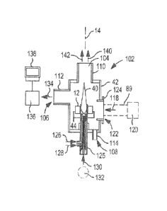
[00124] Referring now to Fig. 15 a microwave inductively coupled plasma source
for
optical-emission spectroscopy 102, which uses a dielectric resonator 12 of the
present
invention, made out of high-density Alumina (A1203) ceramics in the form of a
circular
annulus. The dielectric resonator 12triay be supported within cylindrical
radio-frequency
shield 42 made of metal,. such as aluminum, and has several circular openings
104, 106, and
108 each surrounded with aluminum tubular extensions 110, 112, and 114
respectively. The
tubular extensions 110-114, are designed to have a sufficiently small diameter
and
sufficiently long length to form cylindrical waveguidcs below cutoff, greatly
attenuating the
propagation of microwaves through the extension tubes, as is well understood
in the
microwave art, in order to minimize the leakage of microwave energy outside of
the shield
42.
[00125] Microwave power .118 from waveguide 89 communicating with magnetron
120 is
provided at a frequency of 2,450 MHz an d applied to the dielectric resonator
12 through a
rectangular opening 122 in the shield 42 by the means of a coupler 124. The
resonant
frequency of the dielectric resonator 12 can be finely adjusted by varying the
axial location of
the tuning element 44, made in the form of an aluminum ring, positioned
coaxially with the
ring of dielectric resonator 12.
[00126] A triaxial manifold 125 is directed along the axis 14 centered -within
opening 104
and aligned with inner diameter of dielectric resonator 1.2 and made out of
quartz or alumina
tubing. The triaxial manifold is in the form of a conventional torch which may
be similar to that
.24
CA 02905931 2015-09-11
WO 2014/159590 PCT/US2014/024312
used with inductively coupled plasmas. A plasma cooling gas 126 is applied to
an outer ring
of the triaxial manifold 125 while a plasma auxiliary gas 12$ is applied to
the next inner ring
and the center bore receives the dissolved analytical sample or solid
particles of sample 130
from a sample source 132 to be analyzed. The sample 130 is in the form of an
aerosol, or
discrete particles, entrained in a gas, that may be directly introduced into
the plasma 40.
[00127] Light 134 emitted from the plasma 40 in a direction radial to axis 14
passes
through the tubular extension 112 for analysis by a light sensor 136 coupled
to an analyzing
computer 138 that may determine frequency components of the light 134
according to
methods known in the art. Alternatively or in parallel, for the purposes of
the, so called, axial
OES, light 140, emitted by the plasma 40 in the axial direction of axis 14, is
transferred
through the tubular extension 110 for further spectroscopic analysis by a
similar light sensor
136 (not shown fur clarity). The tubular extension 110 also directs the hot
plasma gases and
chemical products 142 to an exhaust venting system (not shown.) The opening
108 and the
tubular extension 114 allow for air cooling of the plasma generator 12 by
natural convection
or by forced flow of air.
[00]281 The optical emission spectrometer of the present invention preferably
comprises a
plasma generator, the plasma generator comprising a dielectric resonator, a
dispersive element
for dispersing light emitted by the plasma according to the wavelength of the
light, and an optical
detector for detecting the dispersed light.
[00129] Fig. 16 is a simplified schematic cross-sectional view of a mass
spectrometer
incorporating the dielectric resonator of the present invention. Most commonly
used
inductively coupled plasma sources for MS operate at radiofrequencics up to
40M1-1z.
Several designs have been proposed and tested with a goal of extending the
operation of the
plasma sources for MS to microwave frequencies, such as 915MHz or 2,450MHz,
where a
magnetron device could serve as an efficient source of large amount of
microwave power.
The existing analytical results indicate that microwave excited plasma offers
unique
advantages that complement the analytical power of a radio-frequency based
plasma
sources. However, one of the key obstacles in the ability to produce a high
quality analytical
plasma at microwave frequencies has been the lack of a field applicator
capable of
producing a pure inductive coupling to the plasma. All of the designs proposed
to date are
CA 02905931 2015-09-11
WO 2014/159590 PCT/US2014/024312
either dominated by capacitivecoupling or retain a significant amount of
parasitic capacitive
coupling, which has a serious negative impact on the plasma source performance
as
previously outlined. In addition, all of the previous designs require
significant modifications
to the conventional mechanical, optical, and chemical interface to the rest of
the
spectrometer, an interface which has proven itself over many years of
operation of radio-
frequency MS in the field.
[00130] In contrast, the plasma source for MS, based on the field applicator
.according to
the present invention, extends the operation of the conventional radio-
frequency inductively
coupled plasma sources to microwave frequencies, practically eliminating
parasitic
capacitive coupling which has limited previous designs,. while requiring
minimum
modifications to the established mechanical, ion, and chemical interface with
the rest of the
spectrometer. In addition, the extremely low losses of the novel field
applicator, allow for a
complete elimination of the fluid cooling system, thus reducing the size,
cost, and the
-complexity of the spectrometer.
[00131] Fig. 16 shows:asehematie simplified cross-section of a microwave
inductively
coupled plasma source for mass spectrometry 200, which uses a field applicator
12 of the
present invention, made out of high-density Alumina (A1203) ceramic in the
form of a ring.
The microwave inductively coupled plasma source for MS 200 has many components
in
common with the microwave inductively coupled plasma source for OES 102 shown
in Fig.
15, and like components have the same identifiers. Additional components shown
in Fig. 16
will now be described. The sampler cone 201 has a small orifice 202 and the
skimmer cone
.203 has a small orifiee204. The region between the sample cone 20.1 and the
skimmer cone
203 is maintained at a low pressure by exhausting the gas 205 by means of a
vacuum pump
(not shown). The ionized sample 206 enters the low pressure region between the
sample and
skimmer cones through the orifice 202. Ions 207 are further transmitted
through the orifice
204 into the high-vacuum region of the .mass-spectrometer. The mass
spectrometer
comprises ion focusing components 209 which comprise at least one ion focusing
element, a
mass analyser .210 and an ion detector 21.1. There may be two or more stages
of pumping
(not shown) disposed within the mass spectrometer. The mass spectrometer is
controlled by
a controller (not shown), which is preferably a computer. Detected signal from
ion detector
26
CA 02905931 2015-09-11
WO 2014/159590 PCT/US2014/024312
211 is recorded, preferably also using a computer, which may be the same
computer as is
used as the controller. The heated plasma gas 208 which has not penetrated the
orifice 202 is
exhausted through the annular region between the RF shield 42 and the sample
cone 201.
[00132j Preferably the optical emission spectrometer or the mass spectrometer
comprises a
plasma generator according to the present invention wherein the radioftequency
power source
provides between 0.5 and 2 kW of power into the plasma.
[00133] The performance of an optical emission spectrometer according to the
present
invention was compared with that of a conventional ICP optical emission
spectrometer operating
in radial viewing mode. A conventional ICP torch was located within the
central aperture of the
dielectric field applicator, the torch being connected to the gas supplies of
the spectrometer. The
dielectric field applicator and torch were mounted such that the plasma formed
within the central
aperture of the dielectric field applicator was aligned for viewing by a high-
resolution Echelle
spectrometer in radial viewing mode. Advantageously the plasma generator was
operated with
both air and nitrogen without any change to the plasma generator system due to
the unique way
in which the ceramic ring works as both an inductor and a tuning device and
because the
electrical coupling into the plasma is substantially purely inductive with
negligible capacitive
coupling.
[00134] Fig. 17 shows a plot of signal intensity in counts per second (IR) vs.
element
concentration for a range of elements utilizing a range of hard and soft lines
measured using an
optical emission spectrometer of the present invention. The energy sums for
the five lines are:
Ca3968, 9.23 eV (3.12 eV energy of excitation and 6.11 eV energy of
ionization);
Cu2165, 5.73 eV (excitation energy):
Cu3247, 3.82 eV (excitation energy);
Mg2802, 12.07 eV (4.42 eV energy of excitation and 7.65 eV energy of
ionization);
Mn2794, 12.25 eV (4.82 eV energy of excitation and 7.42 eV energy of
ionization).
[00135] Linearity was also examined for a solution containing 3% salt matrix.
The results
obtained are shown in Fig. 18 which indicates that linearity is maintained
despite the presence of
a large concentration of sodium from the salt, which being more easily ionized
can modify the
distribution of detected ionic and atomic lines and line emission levels.
[00136] Fig. 19 (a) to (d) are peak profile plots showing measured peak
intensities from a
27
CA 02905931 2015-09-11
WO 2014/159590 PCT/US2014/024312
multielement standard and baselines which are background signals from measured
blanks
(deionised water), for a conventional argon 1CP source and the plasma source
of the present
invention operating with air. The m ulti element standard contained 0.2ppm Ba
and Mg, !ppm
Cu, 5ppm Ni. Cu and Ni are soft atom lines and give much the same performance
with
conventional argon 1CP and the air plasma source of the present invention. Ba
is a harder ion
line and performs better in the conventional argon 1CP plasma, but the peak
intensity in the air
plasma is only a little less than half that in the argon 1CP plasma. Other
forms of dielectric
resonator are contemplated, two examples of which are presented in Figs. 20
and 21.
[00137] Fig. 20 is a perspective partial cutaway view of a dielectric
resonator which is in
the form of a ceramic ring 12 together with an RF shield 42 in direct contact
with an outer
surface of the dielectric resonator 12. This configuration offers the
advantage of smaller
size and better transfer of heat to the RF shield 42. The surface of the
ceramic ring 12 which
is in contact with the RF shield 42 may be plated with metal.
[00138] Fig. 21 is a perspective partial cutaway view of a dielectric
resonator in the form
of two coaxial ceramic rings 12c and 1.2d, together with two concentric RF
shields. The
outer surface of the larger ring 12c is in direct contact with outer RF shield
42aa. The inner
surface of the smaller ring 12d is in direct contact with inner RF shield 42b.
The plasma 40
may be formed in the annular gap between the rings 12c and 12d.
[00139] Certain terminology is used herein for purposes of reference only, and
thus is not
intended to be limiting. For example, terms such as "upper", "lower", "above",
and "below"
refer to directions in the drawings to which reference is made. Terms such as
"front", "back",
"rear", "bottom" and "side", describe the orientation of portions of the
component within a
consistent but arbitrary frame of reference which is made clear by reference
to the text and
the associated drawings describing the component under discussion. Such
terminology may
include the words specifically mentioned above, derivatives thereof, and words
of similar
import. Similarly, the terms "first", "second" and other such numerical terms
referring to
structures do not imply a sequence or order unless clearly indicated by the
context.
[00140] When introducing elements or features of the present disclosure and
the
exemplary embodiments, the articles "a", "an", "the" and "said" are intended
to mean that
there are one or more of such elements or features. The terms "comprising",
"including"
28
and "having" are intended to be inclusive and mean that there may be
additional elements or
features other than those specifically noted. It is further to be understood
that the method
steps, processes, and operations described herein are not to be construed as
necessarily
requiring their performance in the particular order discussed or illustrated,
unless specifically
identified as an order of performance. It is also to be understood that
additional or alternative
steps may be employed.
[00141] The term "ring" should be understood to generally mean a topological
surface of
genius one and not require nor exclude, for example, a circular profile,
radial symmetry or
particular aspect ratios of with a diameter to height except as explicitly
noted.
[00142] It is specifically intended that the present invention not be limited
to the
embodiments and illustrations contained herein and the claims should be
understood to
include modified forms of those embodiments including portions of the
embodiments and
combinations of elements of different embodiments as come within the scope of
the
following claims.
29
CA 2905931 2019-10-17