Note: Descriptions are shown in the official language in which they were submitted.
CA 02906065 2015-09-11
WO 2014/160498
PCT/US2014/026856
TITLE: FLEXIBLE ELECTRONIC FIBER-REINFORCED COMPOSITE
MATERIALS
CROSS-REFERENCE TO RELATED APPLICATIONS
[0001] This application claims priority to U.S. Provisional Patent Application
Serial
No. 61/780,829 filed March 13, 2013, and U.S. Provisional Patent Application
Serial No.
61/784,968 filed March 14, 2013, which are incorporated herein by reference in
their entirety.
FIELD OF THE INVENTION
[0002] The present disclosure relates generally to multilayer electronic
composites
and in particular to flexible electronic fiber-reinforced composites and
methods of
manufacturing same.
BACKGROUND OF THE INVENTION
[0003] Electronics depend upon precise location and dimensional tolerance of
elements and features such as circuits and traces, even to the micron level,
and are trending to
an even smaller scale. Current flexible electronic technology is based on low
strength, low
modulus, unreinforced plastic film with a high Coefficient of Thermal
Expansion (CTE), low
thermal conductivity and high moisture uptake with attendant problems lack of
dimensional
stability due to moisture swelling and degradation of dielectric properties.
Such plastic films
must be relatively thick to carry out proper function, and have sufficient
mechanical
properties to provide a substrate with low stretch, for dimensional stability
and sufficient
strength and tear resistance to provide sufficient durability. The high
Coefficient of Thermal
Expansion (CTE) provides poor dimensional stability under relatively small
variations in
temperature and the low thermal conductivity causes high temperatures due to
dissipate the
heat generated by power consuming circuit elements. The lack of thermal
stability combined
with, low moisture swelling properties, thus providing a substrate with
insufficient
dimensional stability to withstand fabrication processes, thermal strains and
providing in-
service durability and in stability of electronic elements that require
dimensional stability for
optimum performance.
[0004] The end result is that resolution, durability and stability of printed
electronic
components on flexible substrates is currently limited by the properties of
the substrate.
Ideally, thin flexible substrates should have sufficiently high heat transfer
coefficient to
1
CA 02906065 2015-09-11
WO 2014/160498
PCT/US2014/026856
control the planar directionality of heat flow. Thermal expansion and non-
thermal mechanical
deformation of the substrates can
create instability and damage to electronic circuits.
Moisture resistance may be critical to shield the electronic circuits from
damage and to
provide consistent and optimal dielectric properties, and having a smooth
surface receptive to
printing and/or depositing of electronically conductive material is desirable
in the creation of
electronic structures.
[0005] The inadequacy and instability of currently-available thin film
substrates
creates limitations in the accuracy and size of electronic structures created
from them. As
such, there is a need for thin, flexible, dimensionally stable substrates
usable for flexible
electronic composites. Due to the orientability, in particular composites
composed of
oriented layers of unidirectional engineering fibers, of layered composite
construction such
composites may have their mechanical and thermal expansion properties
engineered to match
or complement the properties of the electronic elements incorporated inside
them or on their
surfaces. Furthermore, the thermal conduction properties can similarly be
optimized for
application specific uniformity or directionality of heat transfer. The
thinness of the
composite substrate reduces strains due bending and flexing of the flexible
electronic
elements, especially on the inner and outer surfaces. Additionally the
multilayer
configuration of the composites allows strain sensitive electronic elements to
be positioned
close to the neutral axis of bending to minimize deformations due to bending
or flexing.
SUMMARY OF THE INVENTION
[0006] In various embodiments of the present disclosure, flexible electronic
composite systems comprise a flexible electronic composite material comprising
at least one
conductive layer and at least one fiber-reinforced laminate layer. Conductive
layers include
non-etched copper films, etched copper films, copper ground plane, copper
power plane,
electronic circuitry, and the like. Fiber-reinforced laminate layers comprise,
for example,
laminates of unidirectional fiber-reinforced tapes with various film layers.
In various
embodiments, fiber-reinforced laminate layers are non-conductive layers. In
other
embodiments, fiber-reinforced laminate layers are conductive, such as by the
presence of
metallic constituents or other conductive materials e.g. carbon nanoparticles
in the resin,
and/or in the fibers, within fiber-reinforced layers.
[0007] In various embodiments, flexible electronic composite systems in
accordance
with the present disclosure may further comprise additional electronic
hardware and/or
software, such as for example, computer chips with written code, batteries,
LED displays,
2
CA 02906065 2015-09-11
WO 2014/160498
PCT/US2014/026856
broadcast coils, pressure-sensitive switches, and the like. Such systems may
comprise final
marketable electronic products or may be further incorporated as electronic
elements within
products requiring electronics, such as for example, pallets having RFID
tracking, or clothing
having entertainment, safety or tracking electronics. In various embodiments,
flexible
electronic composite systems comprise a flexible electronic composite material
incorporated
within or on a consumer, industrial, institutional or government product
requiring an
electronic aspect.
[0008] In various embodiments, unidirectional fiber-reinforced layers form
thin and
smooth substrates suitable for etching or printing of electronic circuitry
thereon. In various
embodiments, composite materials in accordance with the present disclosure
provide smooth
surfaces suitable for etching or printing of electronic circuitry thereon.
[0009] In various embodiments, electronic composite systems of the present
disclosure overcome many of the prior deficiencies of electronic substrates,
such as, low
thermal conductivity, high substrate weight, low substrate durability,
instability and non
uniformity of thermal and non-thermal expansion and shrinkage, and mismatch
between the
thermal expansion properties of the substrate and electronic elements, lack of
moisture
resistance and resulting instability of dielectric stability, and lack of
sufficient smoothness for
printing and deposition of electronic elements and conductive materials.
[0010] In various embodiments, multi-layered flexible electronic composites of
the
present disclosure can be manufactured by repetitive addition of conductive
and/or non-
conductive layers, as desired, to produce multi-layered composites. In various
embodiments,
a method of manufacturing a flexible electronic composite material comprises:
adding a
reinforcing layer onto a conductive layer; optionally curing the composite;
optionally etching
the conductive layer; and optionally adding further conductive and/or non-
conductive layers
thereon.
BRIEF DESCRIPTION OF THE DRAWINGS
[0011] The accompanying drawings are included to provide a further
understanding
of the disclosure and are incorporated in and constitute a part of this
specification, illustrate
embodiments of the disclosure, and together with the description serve to
explain the
principles of the disclosure, wherein:
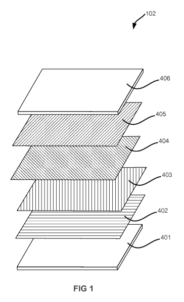
[0012] FIG. 1 illustrates a perspective view of an embodiment of a composite
material in accordance with the present disclosure;
3
CA 02906065 2015-09-11
WO 2014/160498
PCT/US2014/026856
[0013] FIG. 2 illustrates a perspective view of an embodiment of a composite
material in accordance with the present disclosure;
[0014] FIG. 3 illustrates a perspective view of an embodiment of a composite
material in accordance with the present disclosure;
[0015] FIG. 4 illustrates a perspective view of an embodiment of a composite
material in accordance with the present disclosure;
[0016] FIG. 5 illustrates a perspective view of an embodiment of a composite
material in accordance with the present disclosure; and
[0017] FIG. 6 illustrates a front plan view of an embodiment of a circuitry
layer
usable within various composite materials in accordance with the present
disclosure.
DETAILED DESCRIPTION OF THE INVENTION
[0018] The following description is of various exemplary embodiments only, and
is
not intended to limit the scope, applicability or configuration of the present
disclosure in any
way. Rather, the following description is intended to provide a convenient
illustration for
implementing various embodiments including the best mode. As will become
apparent,
various changes may be made in the function and arrangement of the elements
described in
these embodiments without departing from principles of the present disclosure.
[0019] As described in more detail herein, various embodiments of the present
disclosure generally comprise multi-layered flexible electronic composites
comprising at
least one conductive layer and at least one fiber-reinforced laminate layer.
In various
embodiments, the at least one fiber-reinforced laminate layer comprises
directionally aligned
monofilaments. In various embodiments, at least one fiber-reinforced laminate
layer
comprises any number of unidirectional tapes, such tapes having any relative
orientation of
fiber direction between them.
[0020] TABLE 1 provides a glossary of terms and definitions that may be used
in
various portions of the present disclosure.
[0021] TABLE 1: BRIEF GLOSSARY OF TERMS AND DEFINITIONS
Adhesive A resin used to combine composite materials.
Not isotropic; having mechanical and or physical properties which
Anis otropic
vary with direction at a point in the material.
The weight of fiber per unit area, often expressed as grams per square
Areal Weight
meter (g/m2).
4
CA 02906065 2015-09-11
WO 2014/160498
PCT/US2014/026856
A closed vessel for producing a pressurized environment, with or
Autoclave without heat, to an enclosed object which is undergoing a
chemical
reaction or other operation.
Generally defined herein as an intermediate stage in the reaction of
some resin systems. Materials are sometimes pre-cured to this stage,
B-stage
called "prepregs", to facilitate handling and processing prior to final
cure.
Final stage in the reaction of certain resins in which the material is
C-Stage
relatively insoluble and infusible.
To change the properties of a polymer resin irreversibly by chemical
Cure reaction. Cure may be accomplished by addition of curing
(cross-
linking) agents, with or without catalyst, and with or without heat.
Unit of the linear density of a continuous filament or yarn, equal to
Decitex (DTEX)
1/10th of a tex or 9/10th of a denier.
The smallest unit of a fiber-containing material. Filaments usually are
Filament
of long length and small diameter.
An organic material composed of molecules of monomers linked
Polymer
together.
A ready-to-cure sheet or tape material. The resin is partially cured to
Prepreg
a B-stage and supplied to a layup step prior to full cure.
Tow A bundle of continuous filaments.
Ultra-high-molecular-weight polyethylene. A type of polyolefin made
UHMWPE up of extremely long chains of polyethylene. Trade names
include
Spectra and Dyneema0.
Unidirectional tape (or UD tape) ¨ flexible reinforced tapes (also
referred to as sheets) having uniformly-dense arrangements of
Unitape reinforcing fibers in parallel alignment and impregnated with
an
adhesive resin. UD tapes are typically B-staged and can be used as
layers for the composites herein.
PCB Printed Circuit Board
[0022] The above being noted, with reference now to FIG. 1, an embodiment of a
composite material in accordance with the present disclosure is illustrated.
FIG. 1 shows, in
CA 02906065 2015-09-11
WO 2014/160498
PCT/US2014/026856
perspective view, a diagrammatic illustration of a flexible electronic fiber-
reinforced
composite material 102 according to various embodiments of the present
disclosure. In
various embodiments, composite material 102 may be conductive or non-
conductive.
Composite material 102 can be constructed from multiple layers. In various
embodiments,
composite material 102 comprises, for example two, three, four, five, six,
seven, eight, or
more, or many more layers. For example, composite material 102 can comprise at
least one
front surface layer 401, at least one back surface layer 406 and at least one
reinforcing layer,
such as reinforcing layer 402, reinforcing layer 403, reinforcing layer 404,
and reinforcing
layer 405, as shown. In various embodiments, either or both front surface
layer 401 and/or
back surface layer 406 is/are printable with conductive materials, or
otherwise amenable to
deposition of conductive materials.
[0023] Film layers, such as front surface layer 401 and back surface layer
406, are
coatings or films made from materials typical of electronic materials, such
as, polyimide,
PEN, Mylar, glass, amorphous silicone, graphene, organic or inorganic
semiconductors, or
others. Alternate preferred films include metalized films or thin metal
layers. Other alternate
preferred embodiments include interlayers of such films.
Other alternate preferred
embodiments omit such films.
[0024] Reinforcing layers, such as reinforcing layers 402, 403, 404 and 405
illustrated
in FIG. 1, may comprise one or any number of unidirectional tape ("unitape")
sub-layers. A
unidirectional tape is a fiber-reinforced layer having thinly spread parallel
monofilaments
coated by a resin. In various embodiments, resin may be a curable resin or any
type of non-
curing resin. In various embodiments, each unitape sub-layer having parallel
fibers is
inherently directionally oriented, in a dedicated direction, to limit stretch
and provide strength
in such chosen direction. In various embodiments, a two-direction unitape
construction may
feature the first unitape sub-layer disposed at substantially (+/- several
degrees) a 0'
orientation and the second unitape sub-layer disposed at substantially a 90
orientation. In the
same manner, various one-direction configurations, two-direction combinations,
three-
direction combinations, four-direction combinations, and other unitape
combinations, may be
applied to create laminates having a desired directional or non-directional
reinforcement. For
example, in various embodiments, four layers of unidirectional tape sub-layers
may be
laminated in a substantially 0 /+45 /+90 /+135 relative orientation of their
fibers to create
an overall cross-hatched and multi-directional reinforcement.
[0025] In various embodiments, fiber types suitable for reinforcing unitape
sub-layers
include UHMWPE (trade names Spectra, Dyneema), Vectran, Aramid, polyester,
nylon, and
6
CA 02906065 2015-09-11
WO 2014/160498
PCT/US2014/026856
other fibers. Depending on temperature requirements of secondary processing
procedures,
and other considerations, it may be necessary to choose a high melt
temperature fiber such as
Vectran rather than UHMWPE, which melts above 290 F. UHMWPE has advantages
for
flexible electronics including high strength, high thermal conductively, and
excellent flex
fatigue resistance.
[0026] Compared to traditional woven fabrics of the same weight, unitape
reinforcing
layers are significantly thinner, flatter, stronger, and more tear resistant.
Oftentimes, when a
more durable circuit material is desired, a thicker substrate film is chosen.
Rather, for similar
or even improved properties, a substrate that includes the thin fiber-
reinforced unitape layers
in accordance with the present disclosure can be utilized.
[0027] In various embodiments, reinforcing layers within composite materials
of the
present disclosure comprise at least one unidirectional tape having
monofilaments therein, all
of such monofilaments lying in a predetermined direction within the tape,
wherein such
monofilaments have diameters less than about 60 microns and wherein spacing
between
individual monofilaments within an adjoining strengthening group of
monofilaments is
within a gap distance in the range between abutting and/or stacked
monofilaments up to about
300 times the monofilament major diameter. In various embodiments, abutted
and/or stacked
monofilaments form a reinforcing layer that is one or multiple monofilament
layers thick,
depending on strength and modulus considerations of the composite material
design. In
various embodiments, abutting and/or stacked monofilaments produce a
substantially flat
reinforcing layer that is beneficial but not required for this invention.
[0028] In various embodiments, the monofilaments within reinforcing layers,
such as
reinforcing layers 402, 403, 404 and 405, illustrated in FIG. 1, are extruded.
In various
embodiments, reinforcing layers include at least two unidirectional tapes,
each having
extruded monofilaments therein, all of such monofilaments lying in a
predetermined direction
within the tape, wherein such monofilaments have diameters less than about 60
microns and
wherein spacing between individual monofilaments within an adjoining
strengthening group
of monofilaments is within a gap distance in the range between abutting and/or
stacked
monofilaments up to about 300 times the monofilament major diameter. In
various
embodiments, abutted and/or stacked monofilaments form a reinforcing layer
that is one or
multiple monofilament layers thick (stacked), depending on strength and
modulus
considerations of the composite material design.
[0029] In various embodiments, such at least two unidirectional tapes include
larger
areas without monofilaments therein, and wherein such larger areas comprise
laminar
7
CA 02906065 2015-09-11
WO 2014/160498
PCT/US2014/026856
overlays comprising smaller areas without monofilaments. Such smaller areas
can comprise
user-planned arrangements, such as to provide different flexibility between
various regions of
a laminate composite material. In various embodiments, a composite material
may comprise
reinforcing laminate layers wherein a first one of at least two unidirectional
tapes includes
monofilaments lying in a different predetermined direction than a second one
of at least two
unidirectional tapes.
[0030] In various embodiments, a reinforcing layer, such as reinforcing layers
402,
403, 404 and 405, illustrated in FIG. 1, comprises a laminate of
unidirectional tapes wherein
a combination of the different predetermined directions of such at least two
unidirectional
tapes is user-selected to achieve laminate properties having planned
directional
rigidity/flexibility. In various embodiments, a composite material comprises
multiple
laminate segments attached along peripheral joints, such as for example to
provide a bendable
joint in PCB's for electronics. For example, a composite material may comprise
at least one
laminate segment attached along peripheral joints with at least one non-
laminate segment. In
various embodiments, a composite material comprises multiple laminate segments
attached
along area joints.
[0031] In various embodiments, a composite material comprises at least one
laminate
segment attached along area joints with at least one unidirectional tape
segment.
Additionally, in various embodiments, a composite material comprises at least
one laminate
segment attached along area joints with at least one monofilament segment.
Also, in various
embodiments, a composite material further comprises at least one rigid
element.
[0032] With reference now to FIG. 2, an embodiment of composite material 102
is
diagrammatically illustrated in perspective view. Composite material 102
comprises at least
one conducting layer, such as for example, continuous copper layer 414 that
may be etched at
a later time by a manufacturer, sub-manufacturer or end user, or left as is
within the
composite material 102. In various embodiments, such a conductive layer may
comprise any
metalized material, such as copper, that may be masked and etched to form
electrical circuits.
Circuit elements of one or more layers may also be printed using conductive
silver or silver,
gold, copper , zinc, carbon based or semiconductor or organic electrically
active inks or
polymers using printing methods such as gravure, flexo, anilox, screen
printing, ink jet
printing techniques. These inks may be cured using UV, room temperature
catalyst curing or
thermal curing .Typical conductive printable materials are Dupont Solamet PV
412 silver
based for photovoltaic applications for current collection in applications
requiring fine line
resolution, high conductivity and low contact resistance, Dupont 5064 silver
in screen
8
CA 02906065 2015-09-11
WO 2014/160498
PCT/US2014/026856
printing of antennas and general printed electronics requiring high electrical
conductivity,
Dupont 5874 silver based materials and 7105 carbon based materials for screen
printing of
highly stable electrode systems, Dupont 5069 silver and 5067 carbon
flexographic and
Dupont 5064 silver screen printing formulations for printing of conductive
tracks . Flexible
heating elements can be printed using Dupont 7282 Positive Temperature
Coefficient (PTC)
carbon resistor /silver for self-regulating heater applications. Printed
flexible batteries can
also be fabricated using various combinations of silver, carbon and zinc based
inks. For
luminescent and light emoting applications DuPont Luxprint electroluminescent
polymer for
screen printing may be used. For applications requiring more durable or stable
electronic
traces or elements Novacentrics Metalon-JS series silver based inkjet inksõ
Metalon-ICI
series copper oxide reduction inks for screen, inkjet flexo and gravure
printing and Metalon
HPS series silver based inks for screen print applications can be printed and
the resulting
printed elements can be dried, sintered and annealed using Novacentrix
PulseForge photonic
post processing.
[0033] In this illustrated embodiment, composite material 102 may be
constructed by
using one conductive layer portion or multiple conductive layer portions.
[0034] In various embodiments for example, the conductive layer, such as
copper
layer 414, may be disposed in continuous or discontinuous segments or
portions, in planar
arrangement, pressed or adhered against a common adjacent co-planar layer. As
shown in
FIG. 2, composite material 102 comprises a first film layer 412a, laminated
layer 410, a
second film layer 412b, and copper layer 414. In this particular embodiment,
laminated layer
410 is sandwiched between film layers 412a and 412b, although in various other
embodiments, different arrangements of layers may be desirable. In various
embodiments,
such as FIG. 2, laminate layer 410 comprises a multilayered structure, (such
as shown in FIG.
1), comprising a front surface layer 401, reinforcing layer 402, reinforcing
layer 403,
reinforcing layer 404, reinforcing layer 405, and a back surface layer 406,
wherein each
reinforcing layer may comprise any number and orientation of unidirectional
tapes, each
unidirectional tape comprising monofilaments.
[0035] In various embodiments, composite material 102 can be used as a
substrate on
which electrical circuits are printed. The mechanical and thermal dimensional
stability of
various embodiments of the composite material 102 herein allows for ease in
processing.
The fiber type and content as well as choice of surface films create low
thermal expansion
materials or materials with matched thermal expansion for a particular process
or application.
9
CA 02906065 2015-09-11
WO 2014/160498
PCT/US2014/026856
[0036] Referring now to FIG. 3, an embodiment of composite material 102 is
diagrammatically illustrated in perspective view. Composite material 102
comprises a
conductive circuit layer in the form of an etched copper layer 420. The etched-
copper layer
420 may comprise an etching that traces an electronic circuit design. In
various
embodiments, composite material 102 is constructed from multiple layered
portions, whereby
circuits are pre-processed on film substrates and the user adds unidirectional
tape reinforcing
layers as desired. In the embodiment illustrated in FIG. 3, composite material
102 comprises
film layer 412a, laminate layer 410, film layer 412b, etched-copper layer 420,
and film layer
412c. In various other embodiments, different arrangements of conductive and
non-
conductive layers may be desirable. In various embodiments, film layer 412a
and/or film
layer 412c may be amendable to the printing or deposition of metallic
materials thereon. In
various embodiments, such as FIG. 3, laminate layer 410 comprises a
multilayered structure,
(such as shown in FIG. 1), comprising a front surface layer 401, reinforcing
layer 402,
reinforcing layer 403, reinforcing layer 404, reinforcing layer 405, and a
back surface layer
406, wherein each reinforcing layer may comprise any number and orientation of
unidirectional tapes, each unidirectional tape comprising monofilaments.
[0037] With reference now to FIG. 4, an embodiment of composite material 102
is
diagrammatically illustrated in perspective view. Composite material 102
comprises an
additional conductive layer, namely, copper ground plane layer 430. In the
embodiment
illustrated, composite material 102 comprises film layer 412a, copper ground
plane layer 430,
laminate layer 410, film layer 412b, etched-copper layer 420, and film layer
412c. In various
embodiments, a conductive layer is any one of a non-etched metal layer, an
etched-metal
layer, a metal ground plane layer, a metal power plane layer, or an electronic
circuitry layer.
In various embodiments, such as FIG. 4, laminate layer 410 comprises a
multilayered
structure, (such as shown in FIG. 1), comprising a front surface layer 401,
reinforcing layer
402, reinforcing layer 403, reinforcing layer 404, reinforcing layer 405, and
a back surface
layer 406, wherein each reinforcing layer may comprise any number and
orientation of
unidirectional tapes, and wherein each unidirectional tape comprises
monofilaments.
[0038] In various embodiments, copper ground plane layer 430 may be disposed
directly adjacent and co-planar to the etched-copper layer 420, or separated,
as needed, by
any number of intervening film layers or other non-conductive or conductive
layers. In
various embodiments, a conductive layer, such as copper ground plane layer
420, may
operate as a power plane rather than a ground plane. In various embodiments,
composite
material 102 can comprise any number of etched-copper layers 420 and any
number of
CA 02906065 2015-09-11
WO 2014/160498
PCT/US2014/026856
copper ground plane or power plane layers 430, intermixed with any number of
film layers,
laminate layers, or any other conductive and/or non-conductive layers, in any
arrangement, to
produce multilayer PCB's.
[0039] With reference now to FIG. 5, an embodiment of composite material 102
is
diagrammatically illustrated in perspective view. In the manufacturing of
composite material
102, circuits may be added to multiple layers of the composite materials that
return for one or
more lamination steps to produce multilayered flexible composite PCBs.
Composite material
102 comprises film layer 412a, copper ground plane or copper power plane layer
430,
laminate layer 410, film layer 412b, etched-copper layer 420, film layer 412c,
circuitry layer
416, (discussed in more detail below in reference to FIG. 6), and film layer
412d. In various
embodiments, such as FIG. 5, laminate layer 410 comprises a multilayered
structure, (such as
shown in FIG. 1), comprising a front surface layer 401, reinforcing layer 402,
reinforcing
layer 403, reinforcing layer 404, reinforcing layer 405, and a back surface
layer 406, wherein
each reinforcing layer may comprise any number and orientation of
unidirectional tapes, and
wherein each unidirectional tape comprises monofilaments. In various
embodiments,
composite material 102 can comprise any number of etched-copper layers 420,
any number
of circuitry layers 416, and any number of copper ground plane or power plane
layers 430,
intermixed with any number of film layers, laminate layers, or any other
conductive and/or
non-conductive layers, in any arrangement, to produce multilayer PCB's. For
example, in
various embodiments, circuitry layer 416 may appear as the very top layer in a
composite
material 102. In various other embodiments, circuitry layer 416 may appear as
the layer
second to the top within a composite material 102, covered for example by a
single protective
film layer so that various display, antenna, and photovoltaic elements can
still operate, and/or
remain visible through, the protective film.
[0040] Referring now to FIG. 6, a front plan view of an embodiment of an
electronic
circuitry layer 416 is illustrated. Such a circuitry layer, or any conceivable
embodiment of a
circuitry layer, can be used within the composite materials of the present
disclosure. As used
herein, a circuitry layer means an assemblage of electronic components as is
meant to be
distinct from a bare etched circuit design (see element 420 above). In this
particular
embodiment, circuitry layer 416 comprises display 613, antenna 615,
photovoltaic element
617, printed circuitry 619 and discrete sensor 625, although in other
embodiments, any other
componentry and arrangements are within the scope of the present disclosure.
[0041] Composite materials according to the present disclosure typically weigh
between about 10 g/m2 and about 150 g/m2, such as for example, between about
12 g/m2 and
11
CA 02906065 2015-09-11
WO 2014/160498
PCT/US2014/026856
about 133 g/m2. Additionally, composite materials in accordance with the
present disclosure
are typically between about 35 lb/in (35,000 psi) and about 515 lb/in (73,000
psi) in tensile
strength. In various embodiments, composite materials exhibit approximately 3%
elongation
failure and modulus between approximately 1200 lb/in (1,200,000 psi) and
17,000 lb/in
(2,400,000 psi). In various embodiments, composite materials according to the
present
disclosure are typically about 0.001" to about 0.007" in thickness. In various
embodiments,
composite materials in accordance with the present disclosure have fiber or
filament stacking
ranging from side by side or stacked to a center to center distance of
approximately 300-fiber
diameters.
[0042] In various embodiments, a method for manufacturing a flexible composite
material comprises: forming a multilayer composite by adding at least one
reinforcing layer
to at least one conductive layer; and optionally curing the multilayered
composite by
pressure, vacuum and/or heat. In various embodiments, the method further
comprises the
step of etching said conductive layer. In various embodiments, the method
further comprises
the adding of additional conductive and/or non-conductive layers to the
multilayered
composite, either before or after said optional curing. In various
embodiments, non-
conductive film layers are added to the multilayered composite, such as
between any
conductive and/or non-conductive layers, or as outer insulating or protective
layers on one or
both of the outer surfaces of the multilayered composite, before and/or after
said optional
curing.
[0043] In various embodiments, layers within a multilayered composite material
can
be combined and cured together using pressure and temperature, either by
passing the stacked
layers through a heated set of nips rolls, a heated press, a heated vacuum
press, a heated belt
press or by placing the stack of layers into a vacuum lamination tool and
exposing the stack
to heat. Vacuum lamination tools can be covered with a vacuum bag and sealed
to the
lamination tool with a vacuum applied to provide pressure. Moreover, external
pressure,
such as available in an autoclave, can be used in the manufacture of various
embodiments of
the composite materials, herein, and may be used to increase the pressure
exerted on the
layers. The combination of pressure and vacuum that the autoclave provides
results in flat,
thin, and well consolidated materials. Under appropriate circumstances,
considering such
issues as design preference, user preferences, marketing preferences, cost,
structural
requirements, available materials, technological advances, etc., any other
conceivable
lamination method(s) may suffice.
12
CA 02906065 2015-09-11
WO 2014/160498
PCT/US2014/026856
[0044] Composite materials in accordance with the present disclosure have at
least
one or more of the following advantages over traditional monolithic circuit
substrates: high
strength-to-weight and strength-to-thickness, rip-stop, low or matched thermal
expansion,
tailored dielectric properties, and engineered directional in plane and
transverse, out of plane,
thermal conductivities to provide tailored application specific heat transfer
properties.
Additionally, the fiber reinforcement type, quantity, and orientation can be
used to control
and tailor heat flow and directional strength because of the preference for
heat and stress to
travel along the oriented polymer chains in engineering fibers.
[0045] Applications for the composite materials of the present disclosure
include, but
are not limited to, tightly assembled electronic packages, electrical
connections where flexing
is required during use, and electrical connections to replace heavier wire
harnesses. Such
product forms include flexible displays, flexible solar cells, and flexible
antennas, and the
like.
[0046] System embodiments include, but are not limited to:
[0047] Single Layer embodiment: A composite material comprising at least one
conducting layer such as a continuous copper layer that may be etched by the
user;
[0048] Multilayer embodiments: Circuits pre-processed on film substrates
whereby
the manufacturer, sub-manufacturer or user adds the unitape reinforcing layers
and film
layers;
[0049] Layer by layer processed embodiments: Circuits are added to single
layer
materials that return for one or more lamination steps to produce a
multilayered flexible
composite.
[0050] Composite materials in accordance with the present disclosure may
exhibit
one or more of the following properties:
[0051] Strength;
[0052] Low stretch;
[0053] Strength properties that can be engineered to match a required design;
[0054] Low CTE that closely matches that of many materials used in
electronics,
emerging technologies, and nano-technologies;
[0055] Thermal expansion that can be isotropic for uniform, predictable, and
strain
matched thermal expansion. Such property allows for small, fine scale,
circuits and
electronic elements to be fabricated to precise tolerance in fine resolution
and to maintain that
space orientation relative to each other over wide temperature variations so
circuit elements
will maintain design performance tolerance in all directions and in plane;
and/or
13
CA 02906065 2015-09-11
WO 2014/160498
PCT/US2014/026856
[0056] High isotropic or engineered anisotropic in-plane modulus, to provide
low in-
plane mechanical stretch due to mechanical loading, which allows the
mechanical property
analog of the CTE uniformity described above. The low stretch means that
circuit elements
do not change dimensions, and/or the distance between features does not change
due to load.
The dimensional stability provided by the high modulus and engineered
directional properties
improve the resolution and registration of electronic elements and devices
which enable
smaller circuit designs and the incorporation of smaller and tighter
transistor, device or circuit
elements to enable higher density electronic design and integration for
flexible electronics.
Since the performance and reliability of circuits depends upon the special
resolution of the
lateral distances between the electrodes or elements within a device, the
ability to maintain
those resolutions under flex, bending or thermal cycling and the overlay
accuracy and
registration between different circuit or device patterns or layers a low
stretch, dimensionally
stable substrate under mechanical loads, flex due to bending or thermal
strains improves
performance and device stability. For flexible displays the dimensional
stability improves
image resolution and clarity. The low stretch reinforcement enables the use
polymer materials
that have superior environmental stability and resistance to degradation,
superior dielectric
property stability, oxygen and moisture barrier properties or sensitivity to
moisture or oxygen
exposure, resistance to degradation to UV light exposure, or other desirable
properties but
have inadequate mechanical properties that preclude their use as monolithic,
unreinforced
substrates. The ability to incorporate these solves major environmental
stability, service life,
and durability/reliability limitations present in existing substrates for
flexible electronic
applications.
[0057] Thin substrate form factors improve the flexibility of devices and
enable
tighter bend radius for optimum flexibility, bendability and roll ability
while maintaining
operationally reliable flexible electronic elements. Bending strain on the
circuit, device, or
element is proportional to the distance that circuit, device, or element is
from the neutral axis
and the thinner the flexible substrate, the smaller the distances from the
neutral axis which
reduces In various embodiments, the composite material in accordance to the
present
disclosure has an overall thinness, and is amendable to locations of circuits,
devices, or other
elements near the neutral axis so that strains and deformation due to
curvature, distortion,
bending, or crinkling are minimized. Thus, the service life of the circuit,
device, or element
on the composite material of the present disclosure is, in various
embodiments, increased.
The above arrangement can enable incorporation of high-resolution electronic
devices,
14
CA 02906065 2015-09-11
WO 2014/160498
PCT/US2014/026856
elements, circuits, antennas, RF devices, and LEDs into/onto the composite
materials herein
disclosed.
[0058] The structural features of the composite materials of the present
disclosure
stabilize the features of a circuit so there is minimal fatigue and disbanding
of elements in the
circuit due to repeated thermal cycles and load/vibration cycles. Uncontrolled
CTE mismatch
between many electronic elements causes large interfacial stress between the
element and the
substrate, which causes damage and fracturing of the element from the
substrate leading to
device failure.
[0059] Composite materials in accordance with the present disclosure can be
made
from thin homogeneous, uniform unitapes that can produce smooth uniform
laminates that
are also thin, smooth and uniform in properties and thickness. The above
arrangement is due
to the uniform distribution of the monofilaments within the individual unitape
layers. The
unitapes can be oriented with ply angles such that the laminates can either
have uniform
properties in all directions, or the properties can be tailored to match a
device, circuit, or
other requirements.
[0060] The ability to produce a homogeneous, low stretch, low CTE composite
material with unidirectional layer orientation and a flat, smooth surface,
allows for precise
fabrication, deposition, printing, laser ablation, micromachining, etching,
doping, vapor
deposition, coating, 3D printing, application of multiple thin layers of
various electronic
materials and a wide range of other common processes that either require a
flat or uniform
material.
[0061] Applications of composite materials of the present disclosure include,
but are
not limited to: Clothing with integrated antennas and sensors; Conformal
applications for
radars and antennas; EMI, RF and static protection; Structural membranes with
integrated
solar cells, wire traces embedded in the laminate, and on-board planar energy
storage; Low
cost integrated RFID system for package tracking; Flexible circuit boards;
Ruggedize flexible
displays; and Flexible lighting, amongst other applications.
[0062] In various embodiments, conductive or non-conductive additives may be
included in the adhesive/resin of the unitape layers to alter the
Electrostatic Discharge (ESD)
or dielectric (DE) properties of the composite material. In various
embodiments, fire
retardant adhesives or polymers may be used, or fire retardants can be added
to an otherwise
flammable matrix or membrane to improve flame resistance.
[0063] Flame retarding or self-extinguishing matrix resins, or laminating or
bonding
adhesives such as Lubrizol 88111, can be used either by themselves or in
combination with
CA 02906065 2015-09-11
WO 2014/160498
PCT/US2014/026856
fire retardant additives. Examples of retardant additives include: DOW D.E.R.
593
Brominated Resin, DOW Corning 3 Fire Retardant Resin, and polyurethane resin
with
Antimony Trioxide (such as EMC-85/10A from PDM Neptec ltd.), although other
fire
retardant additives may also be suitable. Fire retardant additives that may he
used to improve
flame resistance include Fyrol FR-2, Fyrol HF-4, Fyrol PNX, Fyrol 6, and
SaFRon 7700,
although other additives may also be suitable. Fire retarding or self-
extinguishing features
can also be added to the fibers within unitape layers either by using fire
retardant fibers such
as Nomex or Kevlar, ceramic or metallic wire filaments, direct addition of
fire retardant
compounds to the fiber formulation during the fiber manufacturing process, or
by coating the
fibers with a sizing, polymer or adhesive incorporating fire retardant
compounds listed above
or others as appropriate. Any woven or scrim materials used in the laminate
may be either be
pretreated for fire retardancy by the supplier or coated and infused with fire
retardant
compounds during the manufacturing process.
[0064] In various embodiments, other features that may be imparted to, or
incorporated within, the composite materials of the present disclosure
include, but are not
limited to: Conductive polymer films; Ability to integrate thin flexible
glass; Nano-coating of
the fibers; Integration of nano-materials into the film and matrix;
Integration of EMI, RF, and
static protection; Packaging to produce integration of the electronic device's
functionality
directly into the package; Layered construction analogous to many electrical
circuit concepts
so they are easily and efficiently integrated into the flexible format;
Electrical Resistance;
Thermal conductivity for thermal management and heat dissipation; Fiber
optics; and Energy
storage using multilayered structures.
[0065] In alternate embodiments, filaments may be coated prior to processing
into
unitapes to add functionality such as thermal conductance, electrical
capacitance, and the
like.
[0066] In various other embodiments, metal and dielectric layers may be
included
within the composite to add functionality such as reflection for solar cells,
or capacitance for
energy storage.
[0067] It will be apparent to those skilled in the art that various
modifications and
variations can be made in the present disclosure without departing from the
spirit or scope of
the disclosure. Thus, it is intended that the present disclosure cover the
modifications and
variations of this disclosure provided they come within the scope of the
appended claims and
their equivalents.
16
CA 02906065 2015-09-11
WO 2014/160498
PCT/US2014/026856
[0068] Likewise, numerous characteristics and advantages have been set forth
in the
preceding description, including various alternatives together with details of
the structure and
function of the devices and/or methods. The disclosure is intended as
illustrative only and as
such is not intended to be exhaustive. It will be evident to those skilled in
the art that various
modifications may be made, especially in matters of structure, materials,
elements,
components, shape, size and arrangement of parts including combinations within
the
principles of the disclosure, to the full extent indicated by the broad,
general meaning of the
terms in which the appended claims are expressed. To the extent that these
various
modifications do not depart from the spirit and scope of the appended claims,
they are
intended to be encompassed therein.
17