Note: Descriptions are shown in the official language in which they were submitted.
CA 02907474 2015-09-17
WO 2014/147402 PCT/GB2014/050873
OPTICAL DIODE COMPRISING COMPONENTS MADE
FROM METAMATERIALS
Field
The present disclosure relates to an optical diode and a photovoltaic device.
The present disclosure
also relates to a metamaterial, more specifically, an optical metamaterial.
The present disclosure
also relates to a liquid crystal, more specifically, a cholesteric liquid
crystal. Embodiments relate to a
circular polariser and a circular polarisation splitter. Further embodiments
of the present disclosure
relate to a metamaterial component or layer, or combination of metamaterial
layers, for increasing
the efficiency of a photovoltaic device.
Background
Global photovoltaic (PV) energy generation capacity grew fivefold to 35
gigawatts between 2007 and
2010, with 75% of the capacity available in Europe. Most PV technologies today
are based on
crystalline silicon (Si) wafers, with organic PVs largely being regarded as a
far-in-the-future option.
While silicon absorbs solar light effectively in most of the visible range
(350 ¨ 600 nanometers), it
behaves poorly between 600 ¨ 1,100 nm. In order to compensate for this weak
absorption, most PV
cells have Si wafer thicknesses between 200 ¨ 300 nm, and are typically
referred to as "optically
thick" absorbers. In addition, a pyramidal surface texture is typically
utilized in order to scatter
incoming light over a wide range of angles, thus increasing the effective path
length of the light cell.
However, these approaches have had a significant impact on the basic cost of
PV cells as more
materials and processing is required. Furthermore, for thick solar cells the
photocarrier diffusion
length is comparably short, and thus charge carriers generated away from the
semiconductor
junctions are not effectively collected. This has prevented PV technology from
replacing
conventional fossil fuel technologies for energy generation. Any technological
development that
could decrease the cost of PV cells by at least a factor of two would be a
straightforward revolution
in the industry. Such a development could be achieved by increasing the
absorption efficiency of a
solar cell, so that near-complete light absorption occurs along with
photocarrier current collection.
Some techniques that utilize plasmonics have been investigated so far for
increased efficiency, which
are targeted towards creating thin-film solar cells with thicknesses 1 ¨ 2
micrometers (p.m). For
example, by doping the semiconductor material with 20 ¨ 100 nm diameter
metallic nanoparticles,
1
CA 02907474 2015-09-17
WO 2014/147402 PCT/GB2014/050873
the particles can act as subwavelength scattering elements or near-field
couplers for the incident
solar radiation, increasing the effective scattering cross section.
Another method involves the coupling of incident solar radiation into surface
plasmon polaritons
(SPPs), which are electromagnetic waves that travel along the interfaces of
metals and dielectrics.
This SPP coupling can be achieved for example by corrugating the metallic back
surface of the solar
cell. In all these cases, one of the main challenges which remains is that the
absorption in the
semiconductor material needs to be higher than the plasmon losses in the
metal. However, these
losses become significant for solar wavelengths beyond 800 nm.
It should be emphasized that enhancing the absorption efficiency of weakly
lossy materials offers a
double advantage, as not only smaller quantities of absorbing materials can be
used, but they can
also be of inferior quality, thus in both cases reducing the overall cost of
the device.
Some embodiments of the present disclosure relate to using metamaterials and
metamaterial-based
configurations to address these problems.
Metamaterials are artificially created materials that can achieve
electromagnetic properties that do
not occur naturally, such as negative index of refraction or electromagnetic
cloaking. While the
theoretical properties of metamaterials were first described in the 1960s, in
the past 15 years there
have been significant developments in the design, engineering and fabrication
of such materials. A
metamaterial typically consists of a multitude of unit cells, i.e. multiple
individual elements
(sometimes refer to as "meta-atoms") that each has a size smaller than the
wavelength of operation.
These unit cells are microscopically built from conventional materials such as
metals and dielectrics.
However, their exact shape, geometry, size, orientation and arrangement can
macroscopically affect
light in an unconventional manner, such as creating resonances or unusual
values for the
macroscopic permittivity and permeability.
Some examples of available metamaterials are negative index metamaterials,
chiral metamaterials,
plasmonic metamaterials, photonic metamaterials, etc. Due to their sub
wavelength nature,
metamaterials that operate at microwave frequencies have a typical unit cell
size of a few
millimetres, while metamaterials operating at the visible part of the spectrum
have a typical unit cell
size of a few nanometres. Some metamaterials are also inherently resonant,
i.e. they can strongly
absorb light at certain narrow range of frequencies.
2
CA 02907474 2015-09-17
WO 2014/147402 PCT/GB2014/050873
For conventional materials the electromagnetic parameters such as magnetic
permeability and
electric permittivity arise from the response of the atoms or molecules that
make up the material to
an electromagnetic wave being passed through. In the case of metamaterials,
these
electromagnetic properties are not determined at an atomic or molecular level.
Instead these
properties are determined by the selection and configuration of a collection
of smaller objects that
make up the metamaterial. Although such a collection of objects and their
structure do not "look"
at an atomic level like a conventional material, a metamaterial can
nonetheless be designed so that
an electromagnetic wave will pass through as if it were passing through a
conventional material.
Furthermore, because the properties of the metamaterial can be determined from
the composition
and structure of such small (nanoscale) objects, the electromagnetic
properties of the metamaterial
such as permittivity and permeability can be accurately tuned on a very small
scale.
One particular sub-field of metamaterials are plasmonic materials, which
support oscillations of
electrical charges at the surfaces of metals at optical frequencies. For
example, metals such as silver
or gold naturally exhibit these oscillations, leading to negative permittivity
at this frequency range,
which can be harnessed to produce novel devices such as microscopes with
nanometer-scale
resolution, nanolenses, nanoantennas, and cloaking coatings.
Summary
Aspects of the present disclosure are defined in the appended independent
claims.
The present disclosure details the design of an optical diode using effects
achieved with circular
polarisation. More specifically, the present disclosure relates to
metamaterials and liquid crystals,
more specifically, cholesteric liquid crystals. Notably, embodiments of the
present disclosure may be
formed as layers and may be readily incorporated into conventional devices,
such as photovoltaic
devices, to enhance performance.
Brief description of the drawings
Embodiments of the present disclosure will now be described with reference to
the accompanying
drawings in which:
3
CA 02907474 2015-09-17
WO 2014/147402 PCT/GB2014/050873
Figure 1 shows a schematic layout of an optical diode and photovoltaic device
in accordance with
the present disclosure;
Figure 2 is a schematic of a planar photovoltaic device including an optical
diode in accordance with
embodiments;
Figure 3 shows the simulated field distribution in a planar photovoltaic
device when right-handed
circularly polarised light is incident;
Figure 4 show a comparison of dissipated power for the simulated structure of
Figure 2 with and
without the optical diode according to the present disclosure; and
Figure 5 shows a cylindrical photovoltaic device in accordance with
embodiments.
In the figures, like reference numerals refer to like parts.
Embodiments of the present disclosure relate to effects achieved with optical
radiation. The term
"optical" and "light" are used herein to refer to visible, near- and mid-
infrared wavelengths. That is,
electromagnetic radiation in the range 350 nm to 8 micrometres.
Embodiments also relate to photovoltaic devices but it may be understood from
the following
detailed description that the optical diode in accordance with the present
disclosure may be suitable
for a whole range of applications in which one way transmission and/or one way
reflection of light is
beneficial.
Embodiments also relate to metamaterials or liquid crystals but it can also be
understood from the
following detailed description that the optical diode in accordance with the
present disclosure may
be formed from other non-metamaterial or liquid crystal components such as
commercially available
polarisers and polarising beam splitters having the functionality described.
Detailed description of the drawings
In overview, there is provided an optical diode which is transmissive to one
circular polarisation but
reflective to the opposite circular polarisation. That is, the optical diode
transmits one circular
polarisation but reflects the other circular polarisation. Embodiments take
advantage of the
phenomenon that circular polarised light reverses its polarisation upon
reflection. That is, for
example, a reflection causes right-handed circularly polarised light to become
left-handed circularly
polarised light. Advantageous embodiments, achieve enhanced absorption of
light in a photovoltaic
4
CA 02907474 2015-09-17
WO 2014/147402 PCT/GB2014/050873
material by utilizing a metamaterial structure that allow non-reciprocal
transmission of light. In
further advantageous embodiments, the metamaterial structure is formed from
cholesteric liquid
crystals (CLCs).
CLCs consist of liquid crystal molecules that form helical and periodic
structures along a certain
direction in space. The pitch of a CLC's helix can be adjusted in order to
reflect circularly polarized
light propagating along its axis within a certain frequency range, which is
typically in order of the
hundreds of nanometers. This interesting property of CLCs can be utilized to
fabricate tunable
optical diodes. The inventors have taken advantage of this concept to achieve
significant
enhancements.
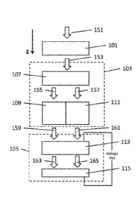
Figure 1 shows a device comprising the optical diode in accordance with the
present disclosure.
In more detail, Figure 1 shows the ordered arrangement of the following
components on a common
optical axis: an antireflection coating 101; an optical diode 103 in
accordance with the present
disclosure; and a photovoltaic device 105. The optical diode 103 comprises a
circular polarisation
splitter 107 having an input aligned with the antireflection coating 101. The
optical diode 103
further comprises a right-hand circular polariser 109 aligned with a first
output of the circular
polarisation splitter 107 and a left-hand circular polariser 111 aligned with
a second output of the
circular polarisation splitter 107. The photovoltaic device 105 comprises a
photovoltaic or absorbing
material 113 aligned with the output of the right-hand circular polariser 109
and the output of the
left-hand circular polariser 111. The solar cell further comprises a reflector
115 aligned with an
output of the photovoltaic material 113. The reflector 115 reflects all
polarisations of light.
In operation, the antireflection coating 101 is arranged to receive first
light 151 such as unpolarised
light, for example, solar light. The antireflection coating 101 outputs second
light 153.
The optical diode 103 has an input and two outputs. The input of the optical
diode is positioned to
receive the second light 153. More specifically, the circular polarisation
splitter 107 of the optical
diode 103 receives the second light 153. The circular polarisation splitter
107 spatially separates the
second light 153 into right-handed circular polarised (RCP) light 155 and left-
handed circular
polarised (LCP) light 157. More specifically, the circular polarisation
splitter 107 outputs the RCP
light 155 on a first optical path and the LCP light 157 on a second optical
path.
5
CA 02907474 2015-09-17
WO 2014/147402 PCT/GB2014/050873
The RCP light 155 is received by the right-handed circular polariser 109. The
right-handed circular
polariser 109 is arranged to transmit right-handed circular polarised light
and reflect left-handed
circular polarised light. The right-handed circular polariser 109 therefore
transmits second RCP light
159 which forms a first output of the optical diode 103.
The LCP light 157 is received by the left-handed circular polariser 111. The
left-handed circular
polariser 111 is arranged to transmit left-handed circular polarised light and
reflect right-handed
circular polarised light. The left-handed circular polariser 111 therefore
transmits second LCP light
161 which forms the second output of the optical diode 103.
The second RCP light 159 and second LCP light 161 are received by the
photovoltaic material 113
which is the photoactive component of the photovoltaic device 105. Any light
not absorbed by the
photovoltaic material 113 ¨ namely, third RCP light 163 and third LCP light
165 ¨ undergoes a first
reflection at reflector 115. The first reflection sends the light back into
the photovoltaic material
113 where further absorption may occur as the light makes a second pass
through the photovoltaic
material 113. However, not all light on the second pass is absorbed by the
photovoltaic material
113. In this case, the light will pass through the photovoltaic material 113
and reach the optical
diode 103 again.
The components are optically aligned such that any of the second RCP light 159
which is reflected by
the reflector 115 (the first reflection), and not absorbed by the photovoltaic
material 113 after the
second pass, is received by the right-handed circular polariser 109. Likewise,
the components are
optically aligned such that any of the second LCP light 161 which is reflected
by the reflector 115,
and not absorbed by the photovoltaic material 113 after the second pass, is
received by the left-
handed circular polariser 111.
Notably, the sense of circular polarisation of circularly polarised light is
reversed by an ordinary
reflection. Therefore, the third RCP light 163 becomes left-handed circular
polarised light after the
first reflection. Any of this light which passes once more through the
photovoltaic material 113 is
therefore reflected by the right-handed circular polariser 109 (i.e. it
undergoes a second reflection)
because the right-handed circular polariser 109 reflects left-handed circular
polarised light.
Therefore a portion of the RCP light 159 makes a third pass through the
photovoltaic material 113.
In fact, it may be understood that a portion of the RCP light 159 may actually
make a fourth pass
through the photovoltaic material 113 following a third reflection at the
reflector 115.
6
CA 02907474 2015-09-17
WO 2014/147402 PCT/GB2014/050873
Likewise, the third LCP light 165 becomes a right-handed circular polarised
light after the first
reflection. Any of this light which passes once more through the photovoltaic
material 113 is
therefore reflected by the left-handed circular polariser 111 (i.e. it
undergoes a second reflection)
because the left-handed circular polariser 111 reflects right-handed circular
polarised light.
Therefore a portion of the LCP light 161 makes a third pass through the
photovoltaic material 113.
In fact, it may be understood that a portion of the LCP light 161 may actually
make a fourth pass
through the photovoltaic material 113 following a third reflection at the
reflector 115.
There is therefore provided an optical diode comprising: a circular
polarisation splitter arranged to
receive at least partially unpolarised light and output right-handed circular
polarised light along a
first optical path and left-handed circular polarised light along a second
optical path; a first circular
polariser arranged on the first optical path, wherein the first polariser is
arranged to transmit right-
handed circular polarised light and reflect left-handed circular polarised
light; and a second circular
polariser arranged on the second optical path, wherein the second polariser is
arranged to transmit
left-handed circular polarised light and reflect right-handed circular
polarised light.
It can therefore be understood that the optical diode functions to redirect
light, which would
otherwise escape the system, back into the photovoltaic material. Accordingly,
more of the first
light 151 is converted into current and then a voltage by the photovoltaic
material. Looking at this
another way, the effective path length of the photovoltaic material is
increased because some light
may make third and fourth passes through the photovoltaic material. Therefore,
the efficiency of a
photovoltaic device may be increased.
In summary, an LCP wave is incident upon the entrance of the device. For
example, the wave may
be propagating along the direction at 600 nm. Provided that the optical diode
is transmissive to left-
handed circular polarised light, this wave will almost fully transmit through
the device, and will
appear at its exit with the same polarization sense (i.e. an LCP wave).
Depending on the absorption
strength of the photovoltaic material after the optical diode, a fraction of
the transmitted power will
be absorbed, while the rest will reflect off the reflector at the end of the
device. The reflector will
invert the sense of polarization of the wave, creating an RCP wave that
propagates in the opposite
direction. Again, a significant fraction of the reflected wave will be
absorbed by the photovoltaic
material as it propagates towards the optical diode. However, the RCP wave
will now perceive the
7
CA 02907474 2015-09-17
WO 2014/147402 PCT/GB2014/050873
optical diode as a reflector, and most of the power will be reflected back
into the photovoltaic
material.
A further schematic of a device in accordance with embodiments is shown in
Figure 2 in which a
solar cell material (absorber region) 213 is sandwiched between a reflector
215 and an optical diode
203, where in this example consists of a layer of a metamaterial ¨ for
example, cholesteric liquid
crystal (CLC) with its pitch tuned to block a certain wavelength range.
From the foregoing, it may be understood that the antireflection coating is
optional. In another
embodiment, the incident unpolarised light is incident directly on the optical
diode 103, 203.
In embodiments, the polarisers comprise a material ¨ such as a metamaterial or
liquid crystal
geometry - that, unlike ordinary reflection, does not invert the sense of
polarisation on reflection. In
these embodiments, the RCP wave has to retain its polarization sense again
after reflection from the
optical diode for causality reasons, as the system is linear and passive.
After this second round of
absorption, most of the remaining energy exits the device. This significantly
increases the absorbed
energy, compared to the device being present in free space without the optical
diode in accordance
with the present disclosure.
In an embodiment, the polarisers and/or polarisation splitter are formed from
metamaterials. That
is, in embodiments at least one of the circular polarisation splitter, first
circular polariser and second
circular polariser comprise an optical metamaterial, wherein the optical
metamaterial comprises a
period component having a dimension no greater than a wavelength of the at
least partially
unpolarised light.
In an embodiment, the periodic component comprises an array of material
elements. In further
embodiments, the array is two-dimensional. The size of the material elements
and/or the spacing of
the material elements are, optionally, sub-wavelength. That is, in an
embodiment each material
element has a first dimension no greater than a wavelength of the at least
partially unpolarised light.
In an embodiment, the first dimension is between 1 nanometre (nm) and 8
micrometres ( m),
optionally, between 1 nm and 100 nm. In an embodiment, the spacing between
adjacent material
elements is between 1 nanometre (nm) and 8 micrometres ( m), optionally,
between 1 nm and 100
nm.
8
CA 02907474 2015-09-17
WO 2014/147402 PCT/GB2014/050873
In an embodiment, the material elements are supported by a host medium. For
example, the at
least one material element may be: at least partially surrounded by the host
medium; located in or
on a surface of the host medium; and/or at least partially embedded in the
host medium. In an
embodiment, the host medium is a dielectric such as silicon or silicon
dioxide.
In an embodiment, the material elements are plasmonic. That is, in an
embodiment, the material
elements comprise a material having a negative dielectric permittivity. In an
embodiment, the
material elements are arranged to resonate at a wavelength of the at least
partially unpolarised
light.
In an embodiment, the material elements are metallic, optionally, at least one
selected from the
group comprising: gold, silver and alumina.
In an embodiment, the circular polariser comprising a planar two-dimensional
array of material
elements made from silver. The material elements are rods and have a width of
20 nm, a length of
100 nm and thickness of 10 nm and adjacent elements are spaced by 50 nm.
However, the skilled person will understand that other sizes and materials may
be used to provide
the effects disclosed herein. For example, the materials elements may be any
plasmonic material at
optical frequencies and may have a size of 1-500 nm. Adjacent material
elements may be spaced by
5-500 nm. The material elements may be ellipsoids, cuboids, spheres,
parallelepipeds, or
combinations of these in groups.
In embodiments, a corresponding left-handed circular polariser is formed from
the same material
elements but rotated
In an advantageous embodiment, the material elements are elongate and
orientated, or "pitched",
with respect to each other to provide optical effects. In an embodiment, the
material elements are
molecules of a liquid crystal. In an embodiment, the metamaterial comprises a
cholesteric liquid
crystal or array of elongate material elements respectively orientated in a
helical configuration. That
is, the elongated material elements are rotated about a propagation axis of
incident light.
The sense of orientation of the respective material elements determines the
sense of polarisation of
the polariser. For example, the same material elements may be used to form the
left and right
9
CA 02907474 2015-09-17
WO 2014/147402 PCT/GB2014/050873
handed circular polarisers however the sense of rotation of the elongated
elements will differ. For
example, the material element may be respectively arranged to form a left-
handed helix or a right-
handed helix.
In an embodiment, the optical diode comprises cholesteric liquid crystals
(CLC). In an embodiment,
the CLC is 1.8 p.m thick (length in the direction of propagation of the light)
with a left handed helix
with pitch p, =315nm . The CLC has an ordinary refractive index of nõ =1.50
and an extraordinary
index of nõ = 1.75. The CLC layers may be assumed to have their optical axes
(their local director) in
the x-y plane, but their orientation depends on their position along the
length of the crystal. The
uniaxial local tensor in the laboratory coordinate system can be written as:
r+ AE COS 2(p AE sin 2(p 0
s(z) = AE sin 2(p ¨ AE COS 2(p 0 (1)
0 0 2
no }
Here = (n,2 +no2)/2 As = (n,2 _no2)/2 and p =2,71-(z ¨ zo)l p , with zo the
location of the starting edge
of the crystal. In this embodiment, the total thickness (length in the
direction of propagation of the
light) of the optical diode is 1.8 p.m and it is aligned with the z-axis of
the domain (the direction of
propagation of the light). Figure 3 shows the result of a simulation of the
planar device shown in
Figure 2 when the incoming radiation is right-hand circularly polarised. More
specifically, Figure 3
shows the field distribution in the photovoltaic material 413 and a single
reflective polariser 410 in
accordance with the present disclosure. The incident wavelength is 500 nm in
free space, and the
absorbing material is modelled with relative permittivity = 3*(1-jtan8),
with tan8 =0.01. The
circular polarizer consists of cholesteric liquid crystals. In this example
the structure is assumed very
large compared to the wavelength in the x & y directions (perpendicular to the
direction of
propagation). The simulation domain includes a 1 p.m long section of air for
improved visualization
of the incoming wave. The absorbing layer is a 1 p.m thick material with a
relative permittivity equal
to E = (1¨ j tan 6), where the loss tangent tans can be varied to simulate
materials with different
absorption strengths.
In embodiments, the cholesteric liquid crystal is made from hydroxypropyl
cellulose or cholesteryl
benzoate having a size of 1 p.m to 1 mm and a pitch of 100 nm to 8 p.m.
CA 02907474 2015-09-17
WO 2014/147402 PCT/GB2014/050873
In another embodiment, the metamaterial polarisers comprise a mix of
cholesteric and nematic
liquid crystals. In an advantageous embodiment, the mix is 70-90% - optionally
80% - cholesteric
and, correspondingly, 30-10% - optionally, 20% - nematic.
The inventors have found that the optical diode in accordance with the present
disclosure
significantly increases the absorbed energy, compared to the device being
present in free space
without the optical diode. Some example results are shown in Figures 3 and 4,
where it may be seen
that, except for very lossy materials, the introduction of the optical diode
doubles the amount of
energy that is absorbed by the material. This scheme is broadband and thus
ideal for existing
photovoltaic devices ¨ in particular, semiconductor solar cells - which suffer
from weak absorption
over a significant portion of the electromagnetic spectrum.
In other embodiments, the optical diode comprises a plurality of layers of
metamaterials. In
embodiments, the optical diode is applied to more complicated systems that
consist of a plurality of
photovoltaic or absorbing later which, optionally, comprise many different
materials. In such cases
the optical diode in accordance with the present disclosure, when placed
immediately after an
existing photovoltaic arrangement, enhances absorption efficiency.
In an embodiment, the optical diode comprises a metamaterial comprising
multiple layers of
cholesteric liquid crystals. Advantageously, the optical metamaterial is
substantially planar.
Accordingly, a layered device may be formed and layering techniques may be
used for fabrication.
Further advantageously, a planar optical diode may be readily coupled with
existing photovoltaic
devices. Notably, in embodiments, the optical diode is passive. That is, it
does not require an
external power source or control systems.
In advantageous embodiments, it may be understand that the first optical path
is substantially
parallel to the second optical path.
Figure 1 shows an embodiment comprises two circular polarisers. However, the
skilled person will
recognise that the optical diode is equally suitable to increase efficiency of
circularly polarised light.
That is, in embodiments, the optical diode operates for one kind of circular
polarization only.
There is therefore provided an optical diode comprising: a circular
polarisation splitter arranged to
receive at least partially unpolarised light and output right-handed circular
polarised light along a
11
CA 02907474 2015-09-17
WO 2014/147402 PCT/GB2014/050873
first optical path and left-handed circular polarised light along a second
optical path; and a circular
polariser arranged on the first optical path, wherein the first polariser is
arranged to transmit one
sense of circularly polarised light and reflect the other sense circularly
polarised light.
However, in advantageous embodiments - such as that shown in Figure 1 - in
order to provide
enhancement independent of the polarization of the incident light, a second
optical diode (but with
inverted orientation compared to the first one) should be placed next to
existing one (transversely to
the direction of propagation of incident light). Incoming unpolarized light
can be first split into left
and right circular polarizations before reaching each diode, using a device
such as a cycloidal
diffractive waveplate (CDW). That is, in an embodiment, the circular
polarisation splitter is formed
from a cycloidal diffractive waveplate. However, the skilled person will
understand that other
circular polarisation splitters may be equally suitable. This device, which
can also be made of
cholesteric liquid crystals, has the ability to split unpolarized light into
two beams of opposite
circular polarizations, which also exit at different locations after the CDW.
This principle enhances
the absorption efficiency for both polarizations, and thus also unpolarized
light.
In embodiments, the CDW comprises liquid crystal molecules which are rotated
along a plane
perpendicular to the direction of light propagation, i.e. the optical axis of
the molecules rotates in
the plane of the layer of material elements. In an embodiment, the molecules
comprise ellipsoidal
molecules of liquid crystal materials such as azobenzene or cinnamates. The
thickness of the layer is
typically between 10 nm to 10 p.m, and it is usually smaller than the spatial
period of the orientation
pattern. In embodiments, the CDW is made using techniques such as photographic
photoalignment.
The optical diode in accordance with the present disclosure may be readily
incorporated in a
photovoltaic device and retrofitted into existing photovoltaic devices. It can
be understood that
there is therefore also provided a photovoltaic device comprising: the optical
diode according to the
present disclosure; a photovoltaic material arranged to receive light on the
first and second optical
paths; and a reflective element arranged to receive light transmitted by the
absorbing element and
redirect that light back towards the optical diode.
The skilled person will understand that any photovoltaic component may be
suitable in accordance
with the present disclosure. For example, in an embodiment, the photovoltaic
component is formed
of at least one selected from the group comprising silicon, germanium, gallium
arsenide and silicon
carbide. In other embodiments, the photovoltaic component is cadmium telluride
or copper indium
12
CA 02907474 2015-09-17
WO 2014/147402 PCT/GB2014/050873
gallium selenide/sulphide. It can be understood from the present disclosure
that other
semiconductors may be equally suitable.
Figure 5 shows an embodiment in which the photovoltaic device is arranged in a
cylindrical
geometry.
The device of Figure 5 has azimuthal symmetry and may be formed by rotating
the one-dimensional
device of Figure 2 by 3600 around its edge (the point where the left edge of
the reflector is located).
Inward propagating, circularly polarized cylindrical waves may be directed
perpendicularly to the
surface of the device, i.e. they are described at the impinging surface by the
expression
= (6 (2)
Here e is the unit vector tangential to the outer surface of the device and 2
is perpendicular to the
x-y plane and out of the page.
The crystal director in this case lies in the 8 plane of the laboratory frame.
The dielectric tensor of
each CLC layer is calculated in the laboratory frame after applying two
rotations. The first is the
rotation along the radial length of the diode by an angle p (r) = 2,71- (r ¨01
p . The length of each
diode is now measured along the r direction instead along the z direction. The
second rotation
occurs in the x-y plane by an angle 9 = tan-' (y / . Thus, the expression for
the permittivity tensor
for the CLC layer is given by
no2 + As sin2 psin2 8 As cos sin cos2 yo As cos sin yo sin
(r,8)= As cos sine cos2 p no2 + As cos2 8sin2 yo ¨As cos silly cos yo (3)
As cos sin yo sine ¨As cos sin yo cos yo no2 + As cos2 p
Along the z direction the device can be extended arbitrarily, or alternated
with a similar device but
with opposite handedness for the diode/polarizer, so that waves of the
opposite polarization are
absorbed. This pair of diodes, coupled with a proper circular polarization
splitter (as indicated in
Figure 1) can absorb all incident polarizations.
13
CA 02907474 2015-09-17
WO 2014/147402 PCT/GB2014/050873
It may therefore be understood that, in an embodiment, the reflective element
is cylindrical and the
photovoltaic material and optical diode are arranged as cylindrical layers
around the reflective
element.
In an embodiment, the photovoltaic device is a solar cell.
The optical diode, metamaterials and/or liquid crystals in accordance with the
present disclosure
may be fabricated by electron beam lithography, focused ion beam lithography,
lift-off processes, or
other lithographic techniques. These techniques may be used to form the
components having the
sub-wavelength parameters and characteristics disclosed herein.
Although embodiments relate to circular polarisation ¨ including circular
polarisers and circular
polarisation beam splitters ¨ it may be understood that embodiments of the
present disclosure may
be equally applicable elliptical radiation. Likewise, the present disclosure
is equally applicable to
metamaterials arranged to provide elliptical or linear polarisation or
polarisation beam splitting, as
defined herein. That is, in an embodiment, there is provided an optical diode
comprising: a
polarisation splitter arranged to receive at least partially unpolarised light
and output first polarised
light along a first optical path and second polarised light along a second
optical path; a first polariser
arranged on the first optical path, wherein the first polariser is arranged to
transmit first polarised
light and reflect second polarised light and wherein the first polariser is a
metamaterial.
Advantageously, the optical diode and photovoltaic device in accordance with
embodiments may be
used as an add-on component existing types of solar panels or photovoltaic
cells. In particular, the
system can be retrofitted in existing photovoltaic devices such as solar
panels. The system is
passive, i.e. it does not require an external power source or an active
control system.
Although aspects and embodiments have been described, variations can be made
without departing
from the inventive concepts disclosed herein.
14