Note: Descriptions are shown in the official language in which they were submitted.
CA 02908205 2015-09-25
WO 2014/156567 <FPHH1823PC>
1
DESCRIPTION
Title of Invention: SPUTTERING DEVICE
Technical Field
[0001] The present invention relates to sputtering
devices, and more particularly, to a sputtering device for
manufacturing hydrogen sensors.
Background Art
[0002] Hydrogen sensors using alloys that exhibit a
change in color (optical characteristic) upon absorption of
hydrogen have been known in the art (see Patent Document 1
by ways of example). A hydrogen sensor is produced by
forming a plurality of thin films of alloy materials, such
as Mg-Ni alloy, on a substrate. Such thin films are formed
using a sputtering device (see Patent Document 2 by way of
example). An inert gas (Ar gas) is introduced into a
vacuum created in the sputtering device, and a target
comprising an alloy material is heated by plasma discharge.
The target is bombarded by ionized Ar, and fine particles
of the alloy material are ejected from the target and form
a film on the substrate. By introducing N2 gas or 02 gas
together with Ar gas, it is possible to carry out reactive
sputtering.
Citation List
Patent Literature
[0003]
Patent Document 1: Japanese Unexamined Patent Publication
No. 2011-219841
Patent Document 2: Japanese Unexamined Patent Publication
No. H05-263228
Summary of Invention
Technical Problem
CA 02908205 2015-09-25
2
[0004] When forming films of a plurality of different
materials on an identical substrate, however, a different
mask needs to be placed between the substrate and the
targets each time a film is to be formed using a different
material, in order to previously delimit a region where the
film is to be formed. A mask has patterned through holes
formed therein, and fine particles of alloy material pass
through the through holes to form a film on a predetermined
region of the substrate. To form a film on a different
region of the substrate, the substrate is taken out of the
sputtering device, and after a mask having a different
through-hole pattern is placed, the substrate is again put
in the sputtering device. Taking out the substrate from
the sputtering device and then placing a new mask in this
manner leads to deterioration of the operation efficiency.
Also, where an easily oxidizable alloy material is used to
form a film, the film is exposed to the atmosphere when the
substrate is taken out of the sputtering device, possibly
causing change of thin film characteristics. In order to
prevent the substrate from being exposed to the atmosphere
when the substrate is taken out of the sputtering device, a
separate vacuum chamber may be provided or a separate
sputtering device may be arranged adjacent to the
sputtering device. Such measures, however, lead to
increase in the overall size of the sputtering device and
require extra space and cost.
[0005] The sputtering device disclosed in Patent
Document 2 is not configured to form films on respective
regions of the substrate because the mask is fixed, and the
substrate and the target are moved to control the film
thickness. To move the target, a large-sized device is
required, leaving the aforementioned space- and cost-
related problems unsolved.
3
[0006] The present invention was made in view of the
aforementioned conventional art, and an object thereof is
to provide a sputtering device which does not require a
substrate to be taken out of the sputtering device or a new
mask to be set in position in cases where films of
different alloy materials are formed on respective regions
of the substrate, and which is superior in terms of space
and cost.
Solution to Problem
[0007] To achieve the object, the present invention
provides a sputtering device including: a vacuum chamber
that is evacuated and hermetically sealed; a plurality of
targets each fixed in the vacuum chamber and comprising a
film forming material; a shield that selectively exposes,
to an inside of the vacuum chamber, only a target among the
plurality of targets out of which a film is to be formed; a
substrate holding unit that holds a substrate on which fine
particles ejected from the target are deposited to form a
film; a first transfer unit that fixedly holds the
substrate holding unit and moves the substrate holding unit
within the vacuum chamber; a mask disposed between the
substrate and the targets; a second transfer unit that
moves the mask within the vacuum chamber; and a plurality
of through-hole units having patterned through holes
penetrating through the mask.
In accordance with a further aspect, a sputtering
device is provided which comprises:
a vacuum chamber that is evacuated and hermetically
sealed;
a plurality of targets each provided in parallel and
each fixed in the vacuum chamber and comprising a film
forming material;
CA 2908205 2019-07-04
3a
a shield that selectively exposes, to an inside of the vacuum
chamber, only a target among the plurality of targets out of which
a film is to be formed;
a substrate holding unit that holds a substrate on which
particles ejected from the target are deposited to form the film;
a first transfer unit that fixedly holds the substrate holding
unit and moves the substrate holding unit within the vacuum
chamber;
a mask disposed between the substrate and the targets;
a second transfer unit that moves the mask within the vacuum
chamber; and
a plurality of through-hole units having patterned through
holes penetrating through the mask,
wherein:
the first transfer unit includes a belt stretched between a
pair of first rollers and positions the substrate in front of one
of the plurality of targets,
the mask is formed as an elongate sheet stretched between a
pair of second rollers,
the first rollers and the second rollers are coupled to output
shafts of first and second motors, respectively,
the plurality of through-hole units are formed in a manner
associated with the targets,
at least one of the targets is associated with two or more of
the plurality of through-hole units; and
each one of the plurality of targets is wider than the through
holes and ejects the particles perpendicularly to a surface of the
substrate.
Advantageous Effects of Invention
[0008] The sputtering device of the present invention does not
require the substrate to be taken out of the sputtering device or a
new mask to be set in position when films of different alloy
materials are formed on respective regions of the substrate, and
yet the sputtering device of the invention is superior in terms of
space and cost. That is, in cases where after the formation of a
film with use
Date Recue/Date Received 2020-07-20
CA 02908205 2015-09-25
4
of a desired target, a film with a different pattern needs
to be formed using a different target, the substrate is
moved to the location of the corresponding target by the
first transfer unit, and if necessary, the mask is moved
using the second transfer unit such that the substrate is
positioned properly with respect to a desired through-hole
unit. Accordingly, films having different patterns can be
formed using a plurality of alloy materials within the
sputtering device.
Brief Description of Drawings
[0009]
FIG. 1 is a sectional view taken along line A-A in
FIG. 2 and schematically illustrating a sputtering device
according to the present invention.
FIG. 2 is a sectional view taken along line D-D in
FIG. 1.
FIG. 3 is a sectional view taken along line A-A in
FIG. 2 and illustrating a state of the sputtering device
different from that illustrated in FIG. 1.
FIG. 4 is a sectional view taken along line B-B in
FIG. 2.
FIG. 5 is a sectional view taken along line B-B in
FIG. 2 and illustrating a state of the sputtering device
different from that illustrated in FIG. 4.
FIG. 6 is a sectional view taken along line C-C in
FIG. 2.
Description of Embodiments
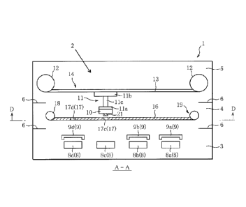
[0010] As illustrated in FIG. 1, a sputtering device 1
according to the present invention has a substantially
hermetically sealed space serving as a vacuum chamber 2.
The vacuum chamber 2 is composed roughly of three regions,
namely, a target section 3, a sputter section 4, and a
substrate section 5. The regions 3 to 5 communicate with
CA 02908205 2015-09-25
each other and may be partitioned to a certain extent by
partition walls 6 insofar as the regions 3 to 5 can
communicate with each other. The vacuum chamber 2 is
evacuated to create a vacuum therein. A plurality of (in
5 the figure, four) targets 8 are fixedly disposed in the
target section 3 forming part of the vacuum chamber 2. The
targets 8 are materials out of which films are formed on a
substrate 10, and more specifically, the targets are masses
of metals (alloys). In the illustrated example, W03, Mg-
Ti, Mg-Ni and Pd are used as targets 8a to 8d,
respectively.
[0011] The targets 8 are associated respectively with
shields 9 (9a to 9d), such as shutters by way of example.
Specifically, the other targets than the one used for film
formation are covered with their respective shields 9, so
that only the target 8 used for film formation is
selectively exposed to the inside of the vacuum chamber 2.
The substrate 10, on which films are formed using the
targets 8, is held by a substrate holding unit 11 disposed
in the substrate section 5. The substrate holding unit 11
includes a gripper ha for gripping the substrate 10 and a
base 11b, and the gripper ha and the base llb are coupled
to each other by an elongate coupler 11c. Among the parts
constituting the substrate holding unit 11, the base lib is
positioned in the substrate section 5. The coupler 11c
extends toward the sputter section 4, and the gripper ha
is positioned in the sputter section 4. Thus, the
substrate 10 held by the gripper ha is located within the
sputter section 4.
[0012] The substrate holding unit 11 is movable within
the vacuum chamber 2 while being fixedly held by a first
transfer unit 14. Specifically, the first transfer unit 14
includes a pair of first rollers 12 disposed within the
CA 02908205 2015-09-25
6
substrate section 5, and a belt 13 stretched between the
first rollers 12. An output shaft of a first motor 15 is
coupled to one of the first rollers 12. Thus, as the first
motor 15 is driven, the first roller 12 that is coupled to
the motor 15 is rotated by the output shaft. As a result,
the driven roller, namely, the other one of the first
rollers 12 also rotates, so that as the belt 13 moves, the
substrate holding unit 11 moves within the vacuum chamber
2. That is, the substrate 10 held by the substrate holding
unit 11 moves within the sputter section 4 along the
direction of movement of the belt 13.
[0013] A mask 16 is
disposed within the sputter section
4 and located between the substrate 10 and the targets 8.
The mask 16 has through holes 17 formed therein in a
patterned manner. Forming through holes in a patterned
manner denotes herein that the through holes 17 form a
desired through-hole pattern when viewed from the target
side. The through holes 17 are formed as discrete through-
hole units 17a to 17f each including one or more through
holes. In the illustrated example, six through-hole units
17a to 17f in total are formed. Also, in the illustrated
example, the through-hole units 17a to 17f each include
three through holes 17 aligned vertically. The mask 16 is
moved within the vacuum chamber 2 by a second transfer unit
19. The second transfer unit 19 includes a pair of second
rollers 18. The mask 16 is formed as an elongate sheet and
stretched between the pair of second rollers 18. An output
shaft of a second motor 20 is coupled to one of the second
rollers 18. Thus, as the second motor 20 is driven, the
second roller 18 that is coupled to the motor 20 is rotated
by the output shaft. As a result, the driven roller,
namely, the other one of the second rollers 18 also
CA 02908205 2015-09-25
7
rotates, so that the mask 16 moves within the vacuum
chamber 2 (sputter section 4).
[0014] The through holes 17 are formed as a plurality of
patterned through-hole units 17a to 17f as mentioned above,
and the through-hole units 17a to 17f are associated with
the targets 8. In the illustrated example, as is clear
from FIG. 2, the through-hole unit 17a is associated with
the target 8a, the through-hole unit 17b is associated with
the target 8b, the through-hole unit 17c is associated with
the target 8c, and the through-hole units 17d to 17f are
associated with the target 8d. That is to say, only the
target 8d is associated with a plurality of through-hole
units 17d to 17f.
[0015] To actually form films on the substrate 10 using
the sputtering device 1 configured as described above, the
procedure explained below is followed.
[0016] First, a substrate is set in the gripper lla of
the substrate holding unit 11, and the vacuum chamber 2 is
evacuated to create a vacuum therein. Then, an inert gas
(Ar gas) is introduced into the vacuum chamber 2. If
necessary, N2 gas or 02 gas is also introduced into the
vacuum chamber. Subsequently, the first motor 15 is driven
to move the belt 13 together with the substrate holding
unit 11. The substrate 10 is positioned first in front of
the Mg-Ni target 8c, as shown in FIG. 1. At this time, the
positioning of the mask 16 is adjusted appropriately using
the second motor 20 so that the through-hole unit 17c
formed in the mask 16 may be situated between the substrate
10 and the target 8c.
[0017] Then, only the shield Sc is opened, and with the
shield Sc kept open, the target 8c is heated by plasma
discharge, whereupon the target 8c is bombarded by ionized
Ar, and fine Mg-Ni particles are ejected from the target Sc
CA 02908205 2015-09-25
8
toward the substrate 10 through the through-hole unit 17c,
with the result that a film is formed according to the
pattern of the through-hole unit 17c. Where the target 8
used is changed, films are formed on the same principle.
The Mg-Ni particles are deposited as a first layer 21 on
the substrate 10.
[0018] Then, as shown in FIG. 3, the substrate 10 is
positioned in front of the Pd target 8d. In the
illustrated example, the through-hole unit 17d of the mask
16 situated between the target 8d and the substrate 10 has
a pattern shape identical with that of the through-hole
unit 17c. The shield 9d alone is opened, and using the
target 8d, a film is formed on the substrate 10. As a
result, a Pd layer as a second layer 22 is formed directly
over the first layer 21. When forming films according to
an identical pattern as in the illustrated case, the
position of the substrate 10 relative to the target 8d to
be used this time is adjusted to be the same as that of the
substrate 10 relative to the previously used target 8c,
whereby the second layer 22 can be formed over the first
layer 21.
[0019] Subsequently, as shown in FIG. 4, the shield 9b
alone is opened, and the substrate 10 is positioned in
front of the Mg-Ti target 8b. The second motor 20 is
driven to adjust the positioning of the mask 16 such that
the through-hole unit 17b is situated between the substrate
10 and the target 8b. Then, as a third layer 23, a Mg-Ti
layer is formed on the substrate 10. In the example
illustrated in FIG. 4, the through-hole unit 17b has a
through-hole pattern different from that of the through-
hole unit 17c, and also the film forming position on the
substrate 10 is slightly shifted. Consequently, the third
layer 23 is formed directly on the substrate 10.
CA 02908205 2015-09-25
9
[0020] Then, as shown in FIG. 5, only the shield 9d is
opened, and the substrate 10 is again positioned in front
of the Pd target 8d. The mask 16 is also moved such that,
in this case, the through-hole unit 17e having a through-
hole pattern identical with that of the through-hole unit
17b is situated between substrate 10 and the target 8d. At
this time, the position of the substrate 10 relative to the
target 8d to be used this time is adjusted to be the same
as that of the substrate 10 relative to the previously used
target 8b. With the substrate thus positioned, a Pd layer
as a fourth layer 24 is formed directly over the third
layer 23.
[0021] Subsequently, as shown in FIG. 6, only the shield
9a is opened, and the substrate 10 is positioned in front
of the W03 target 8a. The second motor 20 is driven to
adjust the positioning of the mask 16 such that the
through-hole unit 17a is situated between the substrate 10
and the target 8a. In the example illustrated in FIG. 6,
the through-hole unit 17a has a through-hole pattern
different from those of the through-hole units 17b and 17c,
and also the film forming position on the substrate 10 is
slightly shifted from those for the targets 8b and 8c.
With the substrate thus positioned, a WO3 layer as a fifth
layer 25 is formed directly on the substrate 10. Where a
Pd layer needs to be formed directly over the fifth layer
25, the through-hole unit 17f may be used to form a film of
Pd.
[0022] In this manner, sputtering can be carried out
while changing the positioning of the mask 16 without the
need to take out the substrate 10 from the sputtering
device 1 each time the target 8 is changed. That is, even
in cases where the pattern of the mask needs to be changed
while films are formed using a plurality of targets 8, the
CA 02908205 2015-09-25
substrate 10 can be moved to the location of the necessary
target 8 by the first transfer unit 14, and if necessary,
the mask 16 is moved using the second transfer unit 19 such
that the substrate 10 is positioned properly with respect
5 to the desired through-hole unit 17. Accordingly, films of
different patterns and different alloy materials can be
formed within the sputtering device 1, and it is possible
to improve the quality of films formed using easily
oxidizable targets, for example. Thus, even in cases where
10 films are formed using different alloy materials on
respective predetermined regions of the substrate 10, it is
not necessary to take out the substrate 10 from the
sputtering device 1 in order to allow a new mask 16 to be
set. If, like Pd in the illustrated example, a certain
target is expected to be used in conjunction with a
plurality of through-hole units, a plurality of through-
hole units 17d to 17f may be prepared for such a target 8d,
and since the target 8 need not be provided for each of the
through-hole units, space and cost can advantageously be
saved.
[0023] In hydrogen sensors, alloys such as the
aforementioned Mg-NI alloy are used for storing hydrogen.
It has been known that a Pd layer additionally deposited as
a catalyst layer serves to improve the hydrogen absorbing
properties. Thus, in the case of the Pd target 8d, the
through-hole unit 17d having the same through-hole pattern
as the through-hole unit 17c with which the Mg-Ni target 8c
is associated may be used to cover the first layer 21
(hydrogen storage layer) with the second layer 22 (catalyst
layer). The aforementioned sputtering device 1 is
therefore especially suited for the manufacture of hydrogen
sensors. In semiconductor applications, sputtering needs
to be performed such that neighboring patterns do no
CA 02908205 2015-09-25
11
overlap each other. In the case of hydrogen sensors, on
the other hand, overlapping of edges of neighboring alloy
layers does not significantly affect the function of
hydrogen sensors because hydrogen sensors are expected to
exhibit a visually observable change in color upon
absorption of hydrogen. It is therefore unnecessary to
provide the sputtering device with a mechanism for
precisely adjusting the distance between the through-hole
units 17 and the substrate 10 or between the targets 8 and
the mask 16 in order to prevent neighboring layers from
overlapping each other, and the sputtering device may have
a simplified structure. Also in this respect, the
aforementioned sputtering device 1 is suited for the
manufacture of hydrogen sensors.
[0024] <Aspects of the Invention>
To achieve the aforementioned object, the present
invention provides a sputtering device including: a vacuum
chamber that is evacuated and hermetically sealed; a
plurality of targets each fixed in the vacuum chamber and
comprising a film forming material; a shield that
selectively exposes, to an inside of the vacuum chamber,
only a target among the plurality of targets out of which a
film is to be formed; a substrate holding unit that holds a
substrate on which fine particles ejected from the target
are deposited to form a film; a first transfer unit that
fixedly holds the substrate holding unit and moves the
substrate holding unit within the vacuum chamber; a mask
disposed between the substrate and the targets; a second
transfer unit that moves the mask within the vacuum
chamber; and a plurality of through-hole units having
patterned through holes penetrating through the mask.
[0025] Preferably, the first transfer unit includes a
belt stretched between a pair of first rollers, the mask is
CA 02908205 2015-09-25
12
formed as an elongate sheet stretched between a pair of
second rollers, the first rollers and the second rollers
are coupled to output shafts of first and second motors,
respectively, the plurality of through-hole units are
formed in a manner associated with the targets, and at
least one of the targets is associated with two or more of
the plurality of through-hole units.
Reference Signs List
[0026]
1: sputtering device
2: vacuum chamber
3: target section
4: sputter section
5: substrate section
6: partition wall
8: target
9: shield
10: substrate
11: substrate holding unit
12: first roller
13: belt
14: first transfer unit
15: first motor
16: mask
17: through hole
18: second roller
19: second transfer unit
20: second motor
21: first layer
22: second layer
23: third layer
24: fourth layer
25: fifth layer