Note: Descriptions are shown in the official language in which they were submitted.
CA 02908514 2015-10-28
52663-149
CHARGING METHOD, MOBILE DEVICE, CHARGING DEVICE, AND
CHARGING SYSTEM
TECHNICAL FIELD
[0001] The present invention relates to the field of communications
technologies, and
in particular, to a charging method, a mobile device, a charging device, and a
charging system.
BACKGROUND
10002] Currently, a user usually connects a mobile device (such as a
mobile phone or a
tablet computer) to an external power supply by using a charging device (such
as a charger),
so as to implement charging of the mobile device; or a user connects a mobile
device to an
external device by using a universal serial bus (USB) USB port, which can also
implement
data exchange between the mobile device and the external device or implement
charging of
the mobile device.
[0003] Current charging circuits cluster on a side of a mobile
device; therefore, as
calculated according to highest conversion efficiency 93% of a charging
circuit in a current
ideal situation, a charging circuit on the side of the mobile device generates
a heat loss of 0.7
W, which causes a heat generation problem during a process of charging the
mobile device,
thereby bringing discomfort to a user in use.
[0004] In addition, with rapid development of mobile devices, battery
capacities of the
mobile devices are increasing, and a shorter charging time is required. If a
conventional
charging circuit continues to be used for charging a mobile device, a charging
time is
excessively long. Therefore, a USB power supply standard is added to a latest
USB standard,
a supply voltage is increased to 20 V, and a supply current is increased to 5
A, so as to quickly
charge a mobile device in a short time. However, because of a significant
increase in the
supply voltage and the supply current, a heat generation problem during a
process of charging
the mobile device is more serious. When a current of 5 A is provided for a
mobile device
according to a latest USB power supply standard, a charging circuit on the
side of the mobile
device generates a heat loss of 7 W, and this heat loss cannot be endured by a
current mobile
CA 02908514 2015-10-28
'52663-149
device.
[0005] To resolve a current heat generation problem during a process
of charging a
mobile device, and to make the mobile device adapt to a charging mode in which
an a supply
voltage and a supply current have been increased, cooling measures such as
graphite attaching
or air cooling is used on the side of the mobile device, so as to reduce a
heat loss generated
during the process of charging the mobile device. However, in this method, a
volume of the
mobile device is increased, and when a charging current keeps increasing, the
heat loss of the
mobile device cannot be reduced radically, which are limitations of the prior
art.
SUMMARY
[0006] Embodiments of the present invention provide a charging method, a
mobile
device, a charging device, and a charging system, which are used to implement
charging of a
mobile device with a high current, reduce a heat loss of the mobile device as
much as
possible, facilitate use of a user, and resolve a problem of limitations in
the prior art.
[0007] According to a first aspect, an embodiment of the present
invention provides a
mobile device, where the mobile device includes a battery and a connector;
where
the connector includes a charging pin and a ground pin; and
when the charging pin establishes a connection to an output pin of a charging
device by using a charging cable or a battery charging stand, the charging pin
receives a first
current signal transmitted by the output pin of the charging device, and
transmits the first
current signal to an anode pin of the battery, so as to charge the battery.
[0008] With reference to the first aspect, in a first possible
implementation manner, the
mobile device further includes an analog switch;
when the charging pin establishes a connection to the output pin of the
charging device by using a charging cable or a battery charging stand, the
analog switch
connects the anode pin of the battery to the charging pin; and
2
CA 02908514 2015-10-28
'52663-149
the charging pin receives the first current signal transmitted by the output
pin
of the charging device, and transmits the first current signal to the anode
pin of the battery by
using the analog switch, so as to charge the battery.
[0009] With reference to the first possible implementation manner of
the first aspect,
in a second possible implementation manner, the mobile device further includes
a charging
circuit and a universal serial bus USB port;
when the charging pin is disconnected from the output pin of the charging
device, the analog switch disconnects the anode pin of the battery from the
charging pin, and
an output pin of the charging circuit is connected to the anode pin of the
battery by using the
analog switch; and
an input pin of the charging circuit is connected to the USB port, receives a
second current signal transmitted by the USB port, and transmits the second
current signal to
the anode pin of the battery by using the output pin of the charging circuit
and the analog
switch, so as to charge the battery.
[0010] With reference to the first aspect or the first or the second
possible
implementation manner of the first aspect, in a third possible implementation
manner, the
mobile device further includes a controller and a voltage converting circuit,
where
with one end connected to the charging pin, and the other end connected to the
controller, the voltage converting circuit is configured to: when the charging
pin establishes a
connection to the output pin of the charging device by using a charging cable
or a battery
charging stand, convert a voltage of the charging pin and then transmit a
converted voltage to
the controller.
100111 With reference to the third possible implementation manner of
the first aspect,
in a fourth possible implementation manner, the controller further includes a
bus port, and the
connector further includes a single-wire or multi-wire bus pin, where
the bus port is connected to the single-wire or multi-wire bus pin of the
3
CA 02908514 2015-10-28
=52663-149
connector by using a bus, and is configured to transmit bus data or a control
signal generated
by the controller, so that the charging device adjusts the output first
current signal after
receiving the bus data or the control signal.
[0012] With reference to the first aspect or any one of the first to
the fourth possible
implementation manners of the first aspect, in a fifth possible implementation
manner, the
ground pin is connected to a first ground pin of the charging device by using
the charging
cable or the battery charging stand; and
the ground pin, a ground pin of the battery and a ground pin of the charging
circuit are connected to each other.
[0013] With reference to the first aspect or any one of the first to the
fifth possible
implementation manners of the first aspect, in a sixth possible implementation
manner, the
connector is specifically a multi-pin port, a multi-contact port, or a port
multiplexed with the
USB port by using the analog switch.
[0014] According to a second aspect, an embodiment of the present
invention provides
a charging device, where the charging device includes a switch charger module
and a charging
circuit, where
the charging circuit includes an input pin and an output pin;
the input pin is connected to an output pin of the switch charger module, and
is
configured to receive a first current signal transmitted by the output pin of
the switch charger
module; and
the output pin establishes a connection to a charging pin of a mobile device
by
using a charging cable or a battery charging stand, so as to use the first
current signal to
charge a battery of the mobile device.
100151 With reference to the second aspect, in a first possible
implementation manner,
the charging circuit further includes a bus port;
4
CA 02908514 2015-10-28
52663-149
=
the bus port is connected to a single-wire or multi-wire bus pin of a
connector
in the mobile device by using a bus, and is configured to receive bus data or
a control signal
transmitted by the mobile device; and
the charging circuit is further configured to adjust the first current signal
according to the bus data or the control signal.
[0016] With reference to the second aspect or the first possible
implementation
manner of the second aspect, in a second possible implementation manner, the
charging circuit
further includes a first ground pin and a second ground pin; where
the first ground pin is connected to a ground pin of the mobile device by
using
the charging cable or the battery charging stand; and
the second ground pin is connected to a ground pin of the switch charger
module.
[0017] With reference to the second aspect or the first or the second
possible
implementation manner of the second aspect, in a third possible implementation
manner, the
charging circuit is specifically a switch charging circuit or a linear
charging circuit.
[0018] According to a third aspect, an embodiment of the present
invention provides a
charging method, where the charging method includes:
receiving, by a charging pin of a connector when the charging pin establishes
a
connection to an output pin of a charging device by using a charging cable or
a battery
charging stand, a first current signal transmitted by the output pin of the
charging device; and
transmitting, by the charging pin, the first current signal to an anode pin of
a
battery, so as to charge the battery.
[0019] With reference to the third aspect, in a first possible
implementation manner,
after the receiving, by a charging pin of a connector when the charging pin
establishes a
connection to an output pin of a charging device by using a charging cable or
a battery
5
CA 02908514 2015-10-28
= 52663-149
charging stand, a first current signal transmitted by the output pin of the
charging device, and
before the transmitting, by the charging pin, the first current signal to an
anode pin of a
battery, the method further includes:
connecting, by an analog switch, the anode pin of the battery to the charging
pin.
[0020] With reference to the first possible implementation manner of
the third aspect,
in a second possible implementation manner, the method further includes:
when the charging pin of the connector is disconnected from the output pin of
the charging device, disconnecting, by the analog switch, the anode pin of the
battery from the
charging pin, and connecting an output pin of a charging circuit to the anode
pin of the battery
by using the analog switch;
receiving, by an input pin of the charging circuit, a second current signal by
using a USB port; and
transmitting, by the input pin of the charging circuit, the second current
signal
to the anode pin of the battery by using the output pin of the charging
circuit and the analog
switch, so as to charge the battery.
[0021] With reference to the third aspect or the first or the second
possible
implementation manner of the third aspect, in a third possible implementation
manner, the
method further includes:
generating, by a controller, bus data or a control signal; and
transmitting, by the controller, the bus data or the control signal to the
charging
device, so that the charging device adjusts the output first current signal.
[0022] According to a fourth aspect, an embodiment of the present
invention provides
a charging system, where the charging system includes the mobile device
according to the
first aspect of the present invention or any one of the six possible
implementation manners of
6
81791944
the first aspect, and the charging device according to the second aspect of
the present
invention or any one of the three possible implementation manners of the
second aspect.
[0022a] According to a further aspect of the present disclosure, there
is provided a
mobile device, wherein the mobile device comprises a battery and a connector,
wherein the
connector comprises a charging pin and a ground pin; and when the charging pin
establishes a
connection to an output pin of a charging device by using a charging cable or
a battery
charging stand, the charging pin receives a first current signal transmitted
by the output pin of
the charging device, and transmits the first current signal to an anode pin of
the battery, and
the charging device comprising a charging circuit, the charging device
supplies the first
current signal by using the charging circuit, so as to charge the battery,
wherein the mobile
device further comprises an analog switch; when the charging pin establishes a
connection to
the output pin of the charging device by using the charging cable or the
battery charging stand,
the analog switch connects the anode pin of the battery to the charging pin;
and the charging
pin receives the first current signal transmitted by the output pin of the
charging device, and
transmits the first current signal to the anode pin of the battery by using
the analog switch, so
as to charge the battery, wherein the mobile device further comprises a
charging circuit and a
universal serial bus USB port; when the charging pin is disconnected from the
output pin of
the charging device, the analog switch disconnects the anode pin of the
battery from the
charging pin, and an output pin of the charging circuit of the mobile device
is connected to the
anode pin of the battery by using the analog switch; and an input pin of the
charging circuit of
the mobile device is connected to the USB port, receives a second current
signal transmitted
by the USB port, wherein the second current signal is smaller than the first
current signal, and
transmits the second current signal to the anode pin of the battery by using
the output pin of
the charging circuit of the mobile device and the analog switch, so as to
charge the battery.
[0022b] Such a mobile device could be implemented in a charging system,
with a
charging device as disclosed herein.
[0022c] Another aspect of the present disclosure relates to a charging
device, wherein
the charging device comprises a switch charger module and a charging circuit,
wherein the
charging circuit comprises an input pin and an output pin; the input pin is
connected to an
7
CA 2908514 2019-05-29
81791944
output pin of the switch charger module, and is configured to receive a first
current signal
transmitted by the output pin of the switch charger module; the output pin
establishes a
connection to a charging pin of a mobile device by using a charging cable or a
battery
charging stand, so as to use the first current signal to charge a battery of
the mobile device,
wherein the charging circuit further comprises a bus port, wherein the bus
port is connected to
a single-wire or multi-wire bus pin of a connector in the mobile device by
using a bus, and is
configured to receive bus data or a control signal transmitted by the mobile
device; and the
charging circuit is further configured to adjust the first current signal
according to the bus data
or the control signal.
[0022d] Another aspect of the present disclosure relates to a charging
method for a
mobile device, wherein the method comprises: receiving, by a charging pin of a
connector
when the charging pin establishes a connection to an output pin of a charging
device by using
a charging cable or a battery charging stand, a first current signal
transmitted by the output pin
of the charging device; and transmitting, by the charging pin, the first
current signal to an
anode pin of the battery, the charging device comprising a charging circuit,
the charging
device supplies the first current signal by using the charging circuit of the
charging device, so
as to charge the battery, wherein after the receiving, by a charging pin of a
connector when the
charging pin establishes a connection to an output pin of a charging device by
using the
charging cable or the battery charging stand, a first current signal
transmitted by the output pin
of the charging device, and before the transmitting, by the charging pin, the
first current signal
to an anode pin of a battery, the method further comprises: connecting, by an
analog switch,
the anode pin of the battery to the charging pin, wherein the method further
comprises: when
the charging pin is disconnected from the output pin of the charging device,
disconnecting, by
the analog switch, the anode pin of the battery from the charging pin, and
connecting an
output pin of a charging circuit of the mobile device to the anode pin of the
battery by using
the analog switch; receiving, by an input pin of the charging circuit of the
mobile device, a
second current signal by using a USB port, wherein the second current signal
is smaller than
the first current signal; and transmitting, by the input pin of the charging
circuit of the mobile
device, the second current signal to the anode pin of the battery by using the
output pin of the
charging circuit of the mobile device and the analog switch, so as to charge
the battery.
7a
CA 2908514 2019-05-29
81791944
[0023] Therefore, by means of an application of the charging method,
the mobile
device, the charging device, and the charging system that are provided in the
embodiments of
the present invention, the mobile device is connected to the charging device
by using a
charging cable or a battery charging stand, and receives a high current
transmitted by the
charging device, so as to charge a battery of the mobile device. In addition,
a charging circuit
that provides a high current is not included in the mobile device, but exists
in the charging
device, which makes the mobile device only receive a high current, so as to
reduce a heat loss
of the mobile device as much as possible. Further, a heat generation problem
during a process
of charging a mobile device in the prior art is resolved, the mobile device is
also made to
adapt to a charging mode in which a supply voltage and a supply current have
been increased,
and a solution in the prior art is also enriched.
BRIEF DESCRIPTION OF DRAWINGS
[0024] FIG. 1 is a schematic structural diagram of a mobile device
according to
Embodiment 1 of the present invention;
[0025] FIG. 2 is a schematic structural diagram of a mobile device
according to
Embodiment 2 of the present invention;
[0026] FIG. 3 is a schematic structural diagram of a mobile device
according to
Embodiment 3 of the present invention;
[0027] FIG. 4 is a schematic structural diagram of a mobile device
according to
Embodiment 4 of the present invention;
[0028] FIG. 5 is a schematic structural diagram of a mobile device
according to
Embodiment 5 of the present invention;
[0029] FIG. 6 is a schematic structural diagram of a charging device
according to an
embodiment of the present invention;
7b
CA 2908514 2019-05-29
CA 02908514 2015-10-28
= 52663-149
[0030] FIG. 7 is a schematic diagram of a connection system that
includes a mobile
device and a charging device according to an embodiment of the present
invention; and
[0031] FIG. 8 is a flowchart of a charging method according to an
embodiment of the
present invention.
DESCRIPTION OF EMBODIMENTS
[0032] To make the objectives, technical solutions, and advantages of
the present
invention clearer, the following further describes the embodiments of the
present invention in
detail with reference to the accompanying drawings.
[0033] The following uses FIG. 1 as an example to describe a mobile
device provided
in an embodiment of the present invention, where FIG. 1 is a schematic
structural diagram of
the mobile device according to this embodiment of the present invention.
[0034] An implementation body of the embodiment shown in FIG. 1 is
the mobile
device. In FIG. 1, the mobile device includes the following components: a
battery 110 and a
connector 120.
[0035] The connector includes a charging pin V1 and a ground pin G1.
[0036] When the charging pin establishes a connection to an output
pin of a charging
device by using a charging cable or a battery charging stand, the charging pin
receives a first
current signal transmitted by the output pin of the charging device, and
transmits the first
current signal to an anode pin of a battery, so as to charge the battery.
100371 Specifically, in this embodiment of the present invention, one end
of the
charging pin of the connector is connected to the anode pin of the battery,
and the other end is
connected to the output pin of the charging device by using the charging cable
or the battery
charging stand.
[0038] The charging cable can specifically endure a current signal of
a high voltage
and a high current. As an example instead of a limitation, the charging cable
can specifically
8
CA 02908514 2015-10-28
.52663-149
endure a high-current signal of 5 A, and can further endure a high-current
signal that exceeds
A in an actual application.
[0039] It should be noted that in this embodiment of the present
invention, the
charging device is a charging device that provides electric energy, includes a
charging circuit
5 and may be connected to a common power supply. As an example instead of a
limitation, to
implement charging with a high current, the charging circuit in the charging
device can
provide a high-current signal, and the first current signal may be
specifically a high-current
signal of 5 A.
[0040] The mobile device in this embodiment of the present invention
may directly
receive, by using the connector, a high current provided by the charging
device, so as to
shorten a charging time. In addition, a charging circuit that provides a high
current does not
exist in the mobile device, but exists in the charging device, which makes the
mobile device
only receive a high current, so as to reduce a heat loss as much as possible.
[0041] Therefore, by means of an application of the mobile device
provided in this
embodiment of the present invention, the mobile device is connected to the
charging device
by using a charging cable or a battery charging stand, and receives a high
current transmitted
by the charging device, so as to charge a battery of the mobile device. In
addition, a charging
circuit that provides a high current is not included in the mobile device, but
exists in the
charging device, which makes the mobile device only receive a high current, so
as to reduce a
.. heat loss of the mobile device as much as possible. Further, a heat
generation problem during
a process of charging a mobile device in the prior art is resolved, the mobile
device is also
made to adapt to a charging mode in which a supply voltage and a supply
current have been
increased, and a solution in the prior art is also enriched.
[0042] Optionally, based on the forgoing embodiment, the mobile
device further
includes an analog switch 210. As shown in FIG. 2, the analog switch in FIG. 2
may be a
single-pole single-throw switch, and may be specifically implemented by using
a field effect
transistor.
[0043] As shown in FIG. 2, a lead EN is led from the charging pin V1
of the
9
CA 02908514 2015-10-28
= 52663-149
connector, and the lead EN is connected to a switch pin of the analog switch.
When the
charging pin V1 establishes a connection to an output pin V1 of a charging
device by using a
charging cable or a battery charging stand, a voltage of the lead EN changes,
which triggers
the analog switch to close, so as to connect the anode pin of the battery to
the charging pin V1
of the connector.
[0044] When the connector is not connected to a charging device, the
analog switch
210 is in a disconnected state, and the ground pin 61 of the connector is
connected to a
ground pin G2 of the battery.
[0045] The charging pin receives a first current signal transmitted
by the output pin of
the charging device, and transmits the first current signal to the anode pin
of the battery by
using the analog switch, so as to charge the battery.
[0046] Based on the forgoing embodiment, the analog switch 210 is
added. When the
charging pin establishes a connection to the output pin of the charging device
by using a
charging cable or a battery charging stand, the analog switch is triggered to
connect the anode
pin of the battery to the charging pin, which can prevent electric leakage of
the connector
when charging is not performed.
[0047] It may be understood that the lead EN is led from the charging
pin V1 of the
connector, and the lead EN is connected to the switch joint of the analog
switch. If the voltage
of the lead EN jumps from a low electrical level to a high electrical level,
it indicates that the
charging pin V1 has established a connection to the output pin V1 of the
charging device by
using the charging cable or the battery charging stand; if the voltage of the
lead EN jumps
from a high electrical level to a low electrical level, it indicates that the
charging pin V1 has
been disconnected from the output pin V1 of the charging device.
[0048] The charging pin V1 establishes a connection to an output pin
V1 of an
external charging device by using a charging cable or a battery charging
stand, so that the
charging pin Vi receives a first current signal, so as to charge the battery.
[0049] Optionally, based on the forgoing embodiment, the mobile
device further
CA 02908514 2015-10-28
'52663-149
includes a charging circuit 310 and a universal serial bus USB port 320. As
shown in FIG. 3,
the analog switch in FIG. 3 is a single-pole double-throw switch, and is
specifically
implemented by using a field effect transistor.
[0050] As shown in FIG. 3, when the connector is not connected to a
charging device,
the anode pin Vbat of the battery is connected to an output pin V2 of the
charging circuit by
using the analog switch, an input pin V3 of the charging circuit is connected
to the USB port,
a ground pin G3 of the charging circuit, the ground pin G2 of the battery and
the ground pin
G1 of the connector are connected to each other, and the charging pin V1 of
the connector
hangs in the air; one end of a voltage converting circuit is connected to the
charging pin V1,
and the other end is connected to a voltage pin Vdet of a controller.
[0051] Based on the forgoing embodiment, the charging circuit and the
universal serial
bus USB port are added. By adding the charging circuit and the USB port, when
the charging
pin V1 is disconnected from an output pin V1 of the charging device, the
battery may still be
charged by using the USB port, and data exchange with another mobile device
may also be
implemented by using the USB port.
[0052] When the charging pin V1 is disconnected from the output pin
V1 of the
charging device, the analog switch disconnects the anode pin Vbat of the
battery from the
charging pin V1, and the output pin V2 of the charging circuit is connected to
the anode pin
Vbat of the battery by using the analog switch.
[0053] The input pin V3 of the charging circuit is connected to the USB
port, receives
a second current signal transmitted by the USB port, and transmits the second
current signal to
the anode pin Vbat of the battery by using the output pin V2 of the charging
circuit and the
analog switch, so as to charge the battery.
[0054] It should be noted that in this embodiment of the present
invention, the
charging circuit 310 in the mobile device is configured to provide a direct
current signal
required by the battery, and specifically, a charging circuit in an existing
mobile device may
be used. In order not to make the mobile device generate an unendurable heat
loss due to
charging with a high current, the charging circuit in the mobile device is set
to provide a low-
11
CA 02908514 2015-10-28
= 52663-149
current signal.
[0055] It should be noted that in this embodiment of the present
invention, the mobile
device (such as a mobile phone or a tablet computer) may further be connected
to another
mobile device (such as a desktop computer or a notebook computer) by using the
USII port.
The another mobile device may be connected to a common power supply, so as to
provide
electric energy for the mobile device in this embodiment of the present
invention. As an
example instead of a limitation, the second current signal may be specifically
a low-current
signal of 2 A. The charging device in this embodiment includes a charging
circuit, where the
charging circuit can provide a high-current signal, for example, a current
signal of 5 A.
[0036] The mobile device in this embodiment of the present invention may
directly
receive, by using the connector, a high current provided by the charging
device, so as to
shorten a charging time. In addition, a charging circuit that provides a high
current does not
exist in the mobile device, but exists in the charging device, which makes the
mobile device
only receive a high current, so as to reduce a heat loss as much as possible.
Further, the
charging circuit in the mobile device is a charging circuit that can maintain
the low-current
signal of 2 A. Therefore, a heat loss of the mobile device can be further
reduced.
[0057] It may be understood that in the mobile device shown in FIG.
3, when the
charging pin V1 establishes a connection to the output pin VI of the charging
device by using
a charging cable or a battery charging stand, a voltage of the lead EN
changes.
[0058] Specifically, as shown in FIG. 3, the lead EN is led from the
charging pin VI
of the connector, and the lead EN is connected to the switch joint of the
analog switch. If the
voltage of the lead EN jumps from a low electrical level to a high electrical
level, it indicates
that the charging pin VI has established a connection to the output pin V1 of
the charging
device by using the charging cable or the battery charging stand; if the
voltage of the lead EN
jumps from a high electrical level to a low electrical level, it indicates
that the charging pin VI
has been disconnected from the output pin V1 of the charging device.
10059] The charging pin V1 establishes a connection to an output pin
V1 of an
external charging device by using a charging cable or a battery charging
stand, so that the
12
CA 02908514 2015-10-28
52663-149
charging pin VI receives a first current signal, so as to charge the battery.
[0060] Optionally, based on the forgoing embodiment, the mobile
device further
includes a controller 410 and a voltage converting circuit 420, as shown in
FIG. 4.
[0061] With one end connected to the charging pin V1, and the other
end connected to
a voltage pin Vdet of the controller, the voltage converting circuit is
configured to: when the
charging pin VI establishes a connection to an output pin of a charging device
by using a
charging cable or a battery charging stand, detect a voltage of the charging
pin, convert the
voltage and then transmit a converted voltage to the controller, so that the
controller
determines that the mobile device established a connection to the charging
device.
[0062] In this embodiment of the present invention, the voltage converting
circuit
adjusts a detected voltage of the charging pin to a voltage that can be
endured by the
controller. For example, the voltage of the charging pin is a voltage of
approximately 10 V,
and the voltage that can be endured by the controller is 2 V; then, the
voltage converting
circuit adjusts the voltage of the charging pin to a voltage of 2 V that can
be endured by the
controller, so that the controller determines that the mobile device has
established a
connection to the charging device.
[0063] Optionally, based on the forgoing embodiment, the controller
further includes a
bus port, the connector further includes a single-wire or multi-wire bus pin,
and the charging
device includes a bus port (not clearly shown in FIG. 4).
[0064] The bus port of the controller is connected to the single-wire or
multi-wire bus
pin by using a bus, and the single-wire or multi-wire bus pin of the connector
is also
connected to a bus pin of the charging device by using the bus. When the
connector is
connected to the charging device, the bus port of the controller is connected
to the bus port of
the charging device by using the single-wire or multi-wire bus pin of the
connector. The bus is
configured to transmit bus data or a control signal generated by the
controller, so that the pin
corresponding to the charging device adjusts an output first current signal
after receiving the
bus data or the control signal.
13
CA 02908514 2015-10-28
= 52663-149
10065] In a preferred embodiment, the bus may be an inter-integrated
circuit I2C bus,
and the single-wire or multi-wire bus pin included in the connector is an I2C
data signal pin
I2C-DATA and an I2C clock pin I2C-CLK, as shown in FIG. 4.
100661 The I2C data signal pin I2C-DATA is connected to the bus port
of the
controller, and is configured to transmit I2C data signal or a control signal
generated by the
controller; the I2C clock pin I2C-CLK is connected to the bus port of the
controller, and is
configured to transmit an I2C clock signal generated by the controller, so
that the bus port of
the charging device adjusts the output first current signal after receiving
the I2C data signal or
the control signal, and the I2C clock signal.
100671 Specifically, the mobile device transmits, by using the I2C data
signal pin I2C-
DATA and the I2C clock pin I2C-CLK of the connector and the I2C bus, the I2C
data signal
or the control signal, and the I2C clock signal to the bus port of the
charging device. In an
example, after the mobile device establishes a connection to the charging
device by using a
charging cable, charging is performed. During a charging process, when the
controller
determines that a first current signal provided by the charging device is so
high that the
mobile device cannot endure, the controller may notify the charging device of
a required first
current signal by transmitting I2C data signal or a control signal, and an I2C
clock signal to
the charging device, so that the charging device adjusts the output first
current signal
according to the I2C data signal or the control signal, and the I2C clock
signal that are
received by the corresponding port.
100681 It may be understood that the foregoing describes working
processes of the bus
port of the controller and the bus pin of the connector by using an I2C bus as
an example. In
an actual application, a connection between the bus port of the controller and
the single-wire
or multi-wire bus pin of the connector is not limited to use of an 12C bus,
and an SPI bus or
the like may also be used.
[0069] Optionally, the ground pin G1 of the connector is connected to
a first ground
pin G1 of the charging device by using the charging cable or the battery
charging stand, and
the ground pin Gl, the ground pin G2 of the battery and the ground pin G3 of
the charging
14
CA 02908514 2015-10-28
52663-149
circuit are connected to each other.
[0070] Optionally, the connector is specifically a multi-pin port, a
multi-contact port,
or a port multiplexed with the USB port by using the analog switch.
[0071] Specifically, the connector in the mobile device provided in
this embodiment
of the present invention may be one of multiple types of ports, such as a
multi-pin port, a
multi-contact port, or a port multiplexed with the USB port by using the
analog switch. As an
example instead of a limitation, in FIG. 5, an analog switch and a USB port
are multiplexed to
serve as a connector. In FIG. 5, the analog switch and the USB port are
multiplexed, so as to
implement functions of the connector in the foregoing embodiment. A charging
process
implemented by the mobile device is as follows: When the mobile device does
not establish a
connection to a charging device, the analog switch is connected to the
charging circuit of the
mobile device by default. The lead EN is led from the voltage pin of the
controller, and the
lead EN is connected to the switch joint of the analog switch. When the mobile
device
establishes a connection to the charging device by using a charging cable or a
battery charging
stand, the analog switch remains connected to the charging circuit when the
controller detects,
by using a USB ID pin, that the mobile device is connected to a computer or
another USB
device by using a USB to perform USB charging; when the controller detects, by
using the
USB ID pin, that the mobile device is charged by using the charging device, a
voltage of the
lead EN jumps from a low electrical level to a high electrical level, and the
analog switch is
disconnected from the charging circuit, and is connected to a Vbat pin of the
battery through
switching, so as to complete charging of the battery. FIG. 5 is only an
example for
implementing the functions of the connector by using another method, and no
limitation is
constituted thereto in an actual application.
[0072] To make the objectives, technical solutions, and advantages of
the present
invention clearer, the following further describes the embodiments of the
present invention in
detail with reference to the accompanying drawings.
[0073] The following uses FIG. 6 as an example to describe a charging
device
provided in an embodiment of the present invention, where FIG. 6 is a
schematic structural
CA 02908514 2015-10-28
= 52663-149
diagram of the charging device according to this embodiment of the present
invention.
[0074] An implementation body of the embodiment shown in FIG. 6 is
the charging
device. As shown in FIG. 6, the charging device includes the following parts:
a switch charger
module 610 and a charging circuit 620.
[0075] In FIG. 6, an output pin V3 and a ground pin G3 of the switch
charger module
are respectively connected to an input pin V2 and a second ground pin G2 of
the charging
circuit, an output pin V1 of the charging circuit is connected to a charging
pin V1 of a mobile
device by using a charging cable or a battery charging stand, and a first
ground pin G1 of the
charging circuit is connected to a ground pin G1 of the mobile device by using
a charging
cable or a battery charging stand.
[0076] In the charging device, the charging circuit includes the
output pin V1 and the
input pin V2.
[0077] The input pin V2 is connected to the output pin V3 of the
switch charger
module, and is configured to receive a first current signal transmitted by the
output pin V3 of
the switch charger module.
[0078] The output pin Vi establishes a connection to the charging pin
VI of the
mobile device by using a charging cable or a battery charging stand, so as to
use the first
current signal to charge a battery of the mobile device.
[0079] Specifically, when the output pin V1 of the charging circuit
establishes a
connection to the charging pin V1 of the mobile device by using a charging
cable or a battery
charging stand, the output pin V1 transmits a carried voltage to the charging
pin V1, which
makes a voltage of a lead EN connected to the charging pin Vi jump, so as to
connect an
analog switch in the mobile device to the charging pin V1, so that the first
current signal is
transmitted to an anode pin Vbat of the battery by using the analog switch, so
as to charge the
battery in the mobile device.
[0080] In this embodiment of the present invention, the charging
cable can specifically
16
CA 02908514 2015-10-28
52663-149
endure a current signal of a high voltage and a high current. As an example
instead of a
limitation, the charging cable can specifically endure a high-current signal
of 5 A, and can
further endure a high-current signal that exceeds 5 A in an actual
application.
[0081] Further, the switch charger module in this embodiment of the
present invention
is configured to: connect to a power supply, receive an alternating current
signal transmitted
by the power supply, convert the alternating current signal into a direct
current signal, and
transmit the direct current signal to the charging circuit.
[0082] The charging circuit is configured to: receive the direct
current signal, convert
the received direct current signal into a direct current signal required by
the battery of the
mobile device, and transmit, by using a charging cable or a battery charging
stand, the direct
current signal required by the battery to the mobile device, where the direct
current signal that
is required by the battery and that is transmitted to the mobile device is a
first current signal.
[0083] The switch charger module is connected to a common power
supply, and
receives an alternating current signal (for example, an alternating current of
220 V)
transmitted by the power supply. The switch charger module converts the
alternating current
signal into a direct current signal (for example, a direct current of 110 V),
and transmits the
direct current signal, which is obtained after conversion, to the input pin V2
of the charging
circuit by using the output pin V3.
[0084] The charging circuit receives, by using input pin V2, the
direct current signal
transmitted by the switch charger module, converts, according to a charge
curve of the battery
of the mobile device, the direct current signal into a direct current signal
required by the
battery, and transmits, by using the output pin V1 of the charging circuit and
a charging cable
or a battery charging stand, the direct current signal required by the battery
to the charging pin
VI of the mobile device.
[0085] Herein, a charge curve of a battery is a characteristic curve of
charging of the
battery. For example, when the battery is empty (a battery level is zero), in
this case, the
battery can receive only a low current for charging, and therefore, the
charging circuit
provides a current signal of a low current for the battery according to the
charge curve of the
17
CA 02908514 2015-10-28
52663-149
battery. When there is a certain amount of electricity in the battery (the
battery level is 20% of
a total battery capacity), in this case, the battery can receive a high
current for charging, and
therefore, the charging circuit provides a current signal of a high current
for the battery
according to the charge curve of the battery.
[0086] It should be noted that in this embodiment of the present invention,
the
charging device is a charging device that provides electric energy and may be
connected to a
common power supply. As an example instead of a limitation, the first current
signal may be
specifically a high-current signal of 5 A. In this embodiment of the present
invention, the
charging circuit that provides a high-current signal is disposed in the
charging circuit;
therefore, the mobile device may directly receive, by using a connector, a
high current
provided by the charging device, so as to shorten a charging time, so that a
heat loss is
reduced as much as possible a high current is disposed in the charging device.
100871 Optionally, the charging circuit further includes a bus port.
[0088] The bus port of the charging circuit is connected to a bus pin
of the connector
in the mobile device, and is configured to receive bus data or a control
signal transmitted by
the mobile device.
[0089] The charging circuit is further configured to adjust the first
current signal
according to the bus data or the control signal.
[0090] In a preferred embodiment, when a bus is an I2C bus, the bus
port of the
charging circuit includes an I2C data signal pin I2C-DATA and an I2C clock pin
I2C-CLK.
[0091] The I2C data signal pin I2C-DATA in the charging circuit is
connected to an
I2C data signal pin I2C-DATA of the connector in the mobile device, and is
configured to
receive I2C data signal or a control signal generated by a controller in the
mobile device.
[0092] The I2C clock pin I2C-CLK in the charging circuit is connected
to an I2C
clock pin I2C-CLK of the connector in the mobile device, and is configured to
receive an I2C
clock signal generated by the controller in the mobile device.
18
CA 02908514 2015-10-28
52663-149
[0093] The charging circuit is further configured to adjust the first
current signal
according to the I2C data signal or the control signal, and the I2C clock
signal.
[0094] Specifically, the mobile device transmits the I2C data signal
or the control
signal, and the I2C clock signal to the charging device by using the I2C data
signal pin I2C-
DA1A and the I2C clock pin 12C-CLK of the connector and the I2C bus. In an
example, after
the mobile device establishes a physical connection to the charging device by
using a charging
cable, charging is performed. During a charging process, when the controller
determines that a
first current signal provided by the charging device is so high that the
mobile device cannot
endure, the controller may notify the charging device of a required first
current signal by
transmitting I2C data signal or a control signal, and an I2C clock signal to
the charging
device, so that the charging device adjusts the output first current signal
according to the I2C
data signal or the control signal, and the I2C clock signal that are received,
and then transmits
an adjusted first current signal to an anode pin V1 of the connector in the
mobile device by
reusing the charging cable.
[0095] It may be understood that the foregoing describes a working process
of the bus
port of the charging circuit by using an I2C bus as an example. In an actual
application, a type
of a bus is not limited to an I2C bus, and may also be an SPI bus or the like.
[0096] Optionally, the charging circuit further includes the first
ground pin G1 and the
second ground pin 02.
[0097] The first ground pin 01 is connected to the ground pin 01 of the
mobile device
by using a charging cable or a battery charging stand.
[0098] The second ground pin 02 is connected to the ground pin G3 of
the switch
charger module.
[0099] Optionally, the charging circuit is specifically a switch
charging circuit or a
linear charging circuit.
[00100] Specifically, in this embodiment of the present invention, a
charging circuit
19
CA 02908514 2015-10-28
= 52663-149
that can provide a high current is disposed in the charging device, so as to
reduce a heat loss
of a mobile device. However, a heat loss of the charging device is easily
caused if a charging
circuit that provides a high current is disposed in the charging device;
therefore, in this
embodiment of the present invention, the charging circuit may be specifically
set as a switch
charging circuit or a linear charging circuit, so as to reduce a heat loss of
the charging device.
Either the switch charging circuit or the linear charging circuit is a circuit
well known to a
person skilled in the art, and therefore, details are not described herein
again.
[00101] Therefore, by means of an application of the charging device
provided in this
embodiment of the present invention, a charging circuit that can provide a
high current is
added in the charging device, to transmit a high current to a mobile device by
using a charging
cable, which makes the mobile device only receive a high current, so as to
reduce a heat loss
of the mobile device as much as possible. Further, a heat generation problem
during a process
of charging a mobile device in the prior art is resolved, the mobile device is
also made to
adapt to a charging mode in which a supply voltage and a supply current have
been increased,
.. and a solution in the prior art is also enriched.
[00102] In the foregoing multiple embodiments, a mobile device and a
charging device
are separately used as implementation bodies to briefly describe charging
processes. Further,
the charging processes described in the foregoing embodiments may be completed
by using a
connection system of a mobile device and a charging device shown in FIG. 7. As
shown in
FIG. 7, the mobile device includes the foregoing multiple components, and a
specific charging
process is as follows:
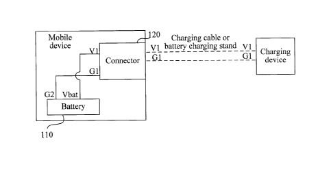
[00103] The foregoing has described a connection relationship between
pins of a
mobile device and those inside a charging device, and details are not
described herein again.
When a charging pin V1 establishes a connection to an output pin VI of the
charging device
by using a charging cable or a battery charging stand, an analog switch
connects an anode pin
Vbat of a battery to the charging pin Vi; the charging pin V1 receives a first
current signal
transmitted by the output pin V1 of the charging device, and transmits the
first current signal
to the anode pin Vbat of the battery by using the analog switch, so as to
charge the battery.
CA 02908514 2015-10-28
52663-149
[00104] Further, the mobile device may further perform exchange
communication with
the charging device by using an I2C bus, and the mobile device transmits an
I2C data signal
and an I2C control signal to the charging device by using the I2C bus, so that
the charging
device adjusts an output current signal.
[00105] The foregoing describes a charging process performed after a mobile
device
establishes a connection to a charging device by using a charging cable. When
the mobile
device is disconnected from the charging device (not shown in the figure), the
mobile device
may receive a second current signal from a USB port by using a charging
circuit of the mobile
device, so as to charge a battery. Charging a battery by using a USB port is
the prior art:
1 0 therefore, details are not described herein again.
[00106] To make the objectives, technical solutions, and advantages of
the present
invention clearer, the following further describes the embodiments of the
present invention in
detail with reference to the accompanying drawings.
[00107] The following uses FIG. 8 as an example to describe a charging
method
provided in an embodiment of the present invention, where FIG. 8 is a
flowchart of the
charging method according to this embodiment of the present invention. The
charging method
provided in this embodiment of the present invention is based on the mobile
device and the
charging device that are described in the foregoing embodiments.
[00108] As shown in FIG. 8, the charging method specifically includes
the following
steps:
[00109] Step 810: When a charging pin of a connector establishes a
connection to an
output pin of a charging device by using a charging cable or a battery
charging stand, the
charging pin receives a first current signal transmitted by the output pin of
the charging
device.
[00110] Further, in this embodiment of the present invention, one end of
the charging
pin of the connector is connected to an anode pin of a battery, and the other
end is connected
to the output pin of the charging device by using a charging cable or a
battery charging stand.
21
CA 02908514 2015-10-28
= 52663-149
The charging cable can specifically endure a current signal of a high voltage
and a high
current. As an example instead of a limitation, the charging cable can
specifically endure a
high-current signal of 5 A, and can further endure a high-current signal that
exceeds 5 A in an
actual application.
1001111 It should be noted that in this embodiment of the present
invention, the
charging device is a charging device that provides electric energy and may be
connected to a
common power supply. As an example instead of a limitation, the first current
signal may be
specifically a high-current signal of 5 A.
[00112] Step 820: The charging pin transmits the first current signal
to an anode pin of
a battery, so as to charge the battery.
[00113] Specifically, the charging pin of the connector is connected
to the anode pin of
the battery. After the charging pin receives the first current signal output
by the output pin of
the charging device, the charging pin transmits the first current signal to
the anode pin of the
battery, so as to charge the battery.
[00114] It may be understood that a mobile device in this embodiment of the
present
invention may directly receive, by using a connector, a high current provided
by a charging
device, so as to shorten a charging time. In addition, a charging circuit that
provides a high
current does not exist in the mobile device, but exists in the charging
device, which makes the
mobile device only receive a high current, so as to reduce a heat loss as much
as possible.
[00115] Optionally, an embodiment of the present invention further provides
another
charging method.
[00116] An analog switch is disposed between the anode pin of the
battery and the
charging pin. When the charging pin of the connector establishes a connection
to the output
pin of the charging device by using a charging cable or a battery charging
stand, the analog
switch connects the anode pin of the battery to the charging pin.
[00117] Further, the charging cable can specifically endure a current
signal of a high
22
CA 02908514 2015-10-28
= 52663-149
voltage and a high current. As an example instead of a limitation, the
charging cable can
specifically endure a high-current signal of 5 A, and can further endure a
high-current signal
that exceeds 5 A in an actual application.
[00118] The charging pin receives the first current signal transmitted
by the output pin
of the charging device.
[00119] Specifically, the charging pin receives, by using a charging
cable or a battery
charging stand, the first current signal output by the output pin of the
charging device.
[00120] It should be noted that in this embodiment of the present
invention, the
charging device is a charging device that provides electric energy and may be
connected to a
common power supply. As an example instead of a limitation, the first current
signal may be
specifically a high-current signal of 5 A.
[00121] The charging pin transmits the first current signal to the
anode pin of the
battery by using the analog switch, so as to charge the battery.
[00122] Specifically, the analog switch connects the charging pin of
the connector to
the anode pin of the battery; therefore, after receiving the first current
signal output by the
output pin of the charging device, the charging pin transmits the first
current signal to the
anode pin of the battery by using the analog switch, so as to charge the
battery.
[00123] It may be understood that a mobile device in this embodiment
of the present
invention may directly receive, by using a connector, a high current provided
by a charging
device, so as to shorten a charging time. In addition, a charging circuit that
provides a high
current does not exist in the mobile device, but exists in the charging
device, which makes the
mobile device only receive a high current, so as to reduce a heat loss as much
as possible.
[00124] Optionally, this embodiment of the present invention further
includes a step in
which when the charging pin of the connector is disconnected from the output
pin of the
charging device, the battery may still be charged by using a USB port. The
mobile device may
also perform data exchange with another mobile device by using the USB port.
23
CA 02908514 2015-10-28
, 52663-149
[00125] When the charging pin is disconnected from the output pin of
the charging
device, the analog switch disconnects the anode pin of the battery from the
charging pin, and
an output pin of the charging circuit is connected to the anode pin of the
battery by using the
analog switch.
[00126] An input pin of the charging circuit receives a second current
signal by using
the USB port.
100127] Specifically, the input pin of the charging circuit is
connected to the USB port
and receives the second current signal by using the USB port.
[00128] Further, in this embodiment of the present invention, the
mobile device (such
as a mobile phone or a tablet computer) may further be connected to another
mobile device
(such as a desktop computer or a notebook computer) by using the USB port. The
another
mobile device may be connected to a common power supply, so as to provide
electric energy
for the mobile device in this embodiment of the present invention. As an
example instead of a
limitation, the second current signal may be specifically a low-current signal
of 2 A.
[00129] The input pin of the charging circuit transmits the second current
signal to the
anode pin of the battery by using the output pin of the charging circuit and
the analog switch,
so as to charge the battery.
[00130] Specifically, the output pin of the charging circuit is
connected to a voltage pin
of the battery by using the analog switch, and the input pin of the charging
circuit is connected
to the USB port; therefore, after receiving the second current signal by using
the USB port,
the input pin of the charging circuit transmits the second current signal to
the battery by using
the output pin of the charging device and the analog switch, so as to charge
the battery.
[00131] It may be understood that a mobile device in this embodiment
of the present
invention may directly receive, by using a connector, a high current provided
by a charging
device, so as to shorten a charging time. In addition, a charging circuit that
provides a high
current does not exist in the mobile device, but exists in the charging
device, which makes the
mobile device only receive a high current, so as to reduce a heat loss as much
as possible.
24
CA 02908514 2015-10-28
52663-149
Further, the charging circuit in the mobile device is a charging circuit that
can maintain the
low-current signal of 2 A. Therefore, a heat loss of the mobile device can be
further reduced.
[00132] Optionally, this embodiment of the present invention further
includes a step of
performing exchange communication by the mobile device with the charging
device by using
a bus.
[00133] A controller generates bus data or a control signal.
1001341 Specifically, during the foregoing process described in step
810 and step 820,
after the mobile device establishes a connection to the charging device by
using a charging
cable, charging is performed. During a charging process, when the controller
determines that a
first current signal provided by the charging device is so high that the
mobile device cannot
endure, the controller generates bus data or a control signal.
[00135] The controller transmits the bus data or the control signal to
a bus port of the
charging device by using a bus port and a single-wire or multi-wire bus pin of
the connector,
so that the charging device adjusts an output first current signal.
[00136] Therefore, by means of an application of the charging method
provided in this
embodiment of the present invention, a mobile device is connected to a
charging device by
using a charging cable, and receives a high current transmitted by the
charging device, so as to
charge a battery of the mobile device. In addition, a charging circuit that
provides a high
current is not included in the mobile device, but exists in the charging
device, which makes
the mobile device only receive a high current, so as to reduce a heat loss of
the mobile device
as much as possible. Further, a heat generation problem during a process of
charging a mobile
device in the prior art is resolved, the mobile device is also made to adapt
to a charging mode
in which a supply voltage and a supply current have been increased, and a
solution in the prior
art is also enriched.
[00137] A person skilled in the art may be further aware that, in
combination with the
examples described in the embodiments disclosed in this specification, units
and algorithm
steps may be implemented by electronic hardware, computer software, or a
combination
CA 02908514 2015-10-28
= 52663-149
thereof To clearly describe the interchangeability between the hardware and
the software, the
foregoing has generally described compositions and steps of each example
according to
functions. Whether the functions are performed by hardware or software depends
on particular
applications and design constraint conditions of the technical solutions. A
person skilled in the
art may use different methods to implement the described functions for each
particular
application, but it should not be considered that the implementation goes
beyond the scope of
the present invention.
[00138] Steps of methods or algorithms described in the embodiments
disclosed in this
specification may be implemented by hardware, a software module executed by a
processor,
or a combination thereof. The software module may reside in a random access
memory
(RAM), a memory, a read-only memory (ROM), an electrically programmable ROM,
an
electrically erasable programmable ROM, a register, a hard disk, a removable
disk, a CD-
ROM, or any other form of storage medium known in the art.
[00139] In the foregoing specific implementation manners, the
objective, technical
solutions, and benefits of the present invention are further described in
detail. It should be
understood that the foregoing descriptions are only specific implementation
manners of the
present invention, but are not intended to limit the protection scope of the
present invention.
Any modification, equivalent replacement, or improvement made without
departing from the
principle of the present invention should fall within the protection scope of
the present
invention.
26