Note: Descriptions are shown in the official language in which they were submitted.
1
CA 02908664 2015-10-02
WO 2015/065081 PCT/KR2014/010335
Description
Title of Invention: CRUM UNIT MOUNTABLE AND DIS-
MOUNTABLE IN CONSUMABLE UNIT OF IMAGE FORMING
APPARATUS AND IMAGE FORMING APPARATUS USING
THE SAME
Technical Field
Hi Aspects of the exemplary embodiments relate to a Customer Replaceable
Unit
Monitor (CRUM) unit mountable and dismountable in a consumable unit of an
image
forming apparatus and an image forming apparatus using the same, and more par-
ticularly, to a CRUM unit which extracts power from a clock signal and an
image
forming apparatus using the same.
Background Art
[2] With the development of electronic technology, various types of
electronic products
have been developed. In particular, as computers are used widely, the
distribution rate
of computer peripheral devices has also been increasing. The computer
peripheral
devices refer to devices which improve usability of computers, and include
such image
forming apparatuses as a printer, a scanner, a copier, an MFP, etc.
[31 The image forming apparatuses use an ink or a toner to print an image
on a paper. An
ink or a toner is used every time an image forming job is performed and used
up if it is
used for more than a predetermined time. In this case, a unit which stores the
ink or the
toner should be replaced. As such, a part or an element which is replaced in
the process
of using an image forming apparatus is referred to as a consumable unit or a
re-
placeable unit. For convenience of explanation, it will be referred to as a
consumable
unit in this specification.
[4] The consumable unit includes not only a unit which should be replaced
when it is
used up, such as an ink or a toner, but also a unit which should be replaced
after a pre-
determined period of time since its properties change as time goes by and
thus, high
printing quality cannot be expected. That is, the consumable unit may also
include
such parts as a color developer and an intermediate transfer belt. Such
consumable
units should be replaced regularly at an appropriate replacement time.
[51 The replacement time may be determined using a use condition index.
The user
condition index represents the degree of use of an image forming apparatus,
and may
be the number of papers which are printed and output from an image forming
apparatus, the number of dots forming an image, etc. An image forming
apparatus may
count the number of papers or dots to determine the replacement time of each
CA 02908664 2016-04-29
2
consumable unit.
[6] Recently, in order to allow a user to determine the replacement time of
each unit ac-
curately, a CRUM unit may be mounted or dismounted in each consumable unit.
[7] If a consumable unit is mounted on an image forming apparatus, a CRUM
unit and
the image forming apparatus are able to communicate with each other through
each
terminal. The CRUM unit includes a power terminal to receive power provided
from
the image forming apparatus. Accordingly, the power provided from the image
forming apparatus is transmitted to the power terminal, and the CRUM unit may
operate by receiving the power from the power terminal.
[8] However, considering the structural features, the presence of a power
terminal to
provide power may increase the number of interlaces of the CRUM unit. The in-
creasing number of terminals or interfaces also increases the size of the CRUM
unit,
influencing the costs of the CRUM unit.
[9] In addition, as the power is supplied even during a pause in operation,
when data is
not received or transmitted through the power terminal, the power consumption
of the
image forming apparatus increases. In order to overcome the above
disadvantages, it
has been suggested to remove the power terminal and use only two terminals
which
combine data with a clock. However, unlike the case where data and clock are
separately embodied, an interface circuit of a main board needs to be
constructed using
an analog method, and therefore, there are drawbacks of complicated circuit
map and
limitation of speed, or the like.
[10] It is an object of the present invention to address the abovementioned
disadvantages.
Disclosure of Invention
Technical Problem
[11]
[12] An aspect of the exemplary embodiments relates to a CRUM unit which is
configured to extract power from a clock signal which is received from an
image
forming apparatus and an image forming apparatus using the same.
Solution to Problem
[13] According to an exemplary embodiment, the CRUM unit includes a power
extracting
circuit configured to, when a clock signal is received from an image forming
apparatus, extract power from a high value of the clock signal and store the
power in a
capacitive element; and a controller configured to operate using the extracted
power,
wherein the clock signal has a first pulse width in a data section where a
data signal is
received and transmitted, and has a second pulse width which is different from
the first
3
CA 02908664 2015-10-02
WO 2015/065081 PCT/KR2014/010335
pulse width in an pause section where a data signal is not received.
[14] Reference is made to a power extracting circuit, which will be
understood to refer
also to a charge extracting circuit, for supply of charge to the capacitive
element, to
store the charge or extracted charge in the capacitive element.
[15] In this case, the first pulse width of the clock signal may be greater
than the second
pulse width.
[16] The clock signal may be characterized by that a high value and a low
value re-
peatedly alternate in the data section with a first cycle or the high value
and the low
value repeatedly alternate in the pause section with a second cycle which is
different
from the first cycle.
[17] The first cycle may be greater than the second cycle.
[18] The controller may receive and transmit a data signal from the image
forming
apparatus according to the clock signal and manage a memory.
[19] The controller, when it is determined that the pause section is
changed to the data
section based on the clock signal, may transmit/receive the data signal in the
data
section.
[20] The controller, when a high value and a low value of the clock signal
repeatedly
alternate in the pause section and a section where one of the high value and
the low
value is maintained exceed a predetermined a first time, may determine that
the data
section is changed to the data section, and when a high value and a low value
of the
clock signal repeatedly alternate in the data section and a section where one
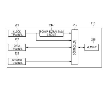
of the high
value and the low value is maintained is smaller than the first time, may
determine that
the data section is changed to the pause section.
[21] The controller, when a high value and a low value of the clock signal
repeatedly
alternate in the pause section and a section where a low value of the clock
signal is
maintained exceeds a predetermined first time, may determine that the time
when the
section exceeds the first time as a time when reception/transmission of the
data signal
starts, and when a high value and a low value of the clock signal repeatedly
alternate in
the data section or the pause section and a section where a high value of the
clock
signal is maintained exceeds a predetermined second time, is operable to
determine
that the time when the section exceeds the second time as a time when
reception of the
data signal ends.
[22] The memory and the controller may consist of one integrated chip, IC.
[23] The power extracting circuit may include a switching element
configured to pass a
clock signal having the high value from among the received clock signals, and
a ca-
pacitive element configured to be recharged by the clock signal which is
passed from
the switching element.
[24] The switching element may be at least one of a diode and a transistor.
4
CA 02908664 2015-10-02
WO 2015/065081 PCT/KR2014/010335
[25] The CRUM unit may further include a data terminal configured to
transmit/receive
the data signal which is divided to a data section and a pause section, when
the CRUM
unit communicates with a main body of the image forming apparatus, a clock
terminal
configured to receive the clock signal from the main body, and a ground
terminal
configured to be connected to a ground terminal of the main body of the image
forming apparatus.
[26] The CRUM may further include a power terminal which is connected to a
power
terminal of the main body of the image forming apparatus, wherein the power
terminal
of the CRUM unit may maintain an inactive state.
[27] The clock signal may have a third width which is different from the
first pulse width
in an idle section where a data signal is not received and transmitted.
[28] According to another exemplary embodiment, a CRUM unit includes a data
terminal
configured to transmit/receive the data signal which is divided to a data
section and an
pause section, when the CRUM unit communicates with a main body of the image
forming apparatus, a clock terminal configured to receive the clock signal for
de-
termining whether the data signal is received or transmitted from the main
body, and a
ground terminal configured to be connected to a ground terminal of the main
body of
the image forming apparatus, a power extracting circuit configured to extract
power
from a high value of the clock signal and store in a capacitive element, and a
controller
configured to be operable using the extracted power, wherein the clock signal
has a
first pulse width in a data section where a data signal is received and
transmitted, and
has a second pulse width which is different from the first pulse width in an
pause
section where a data signal is not received.
[29] According to an exemplary embodiment, an image forming apparatus
includes a
main body having a main controller which is configured to control an operation
of the
image forming apparatus, a consumable unit configured to be mounted on the
main
body to operable to communicate with the main controller, and a CRUM unit
configured to store information on the consumable unit, wherein the main
controller is
configured to transmit a clock signal where a high value and a low value
repeatedly
alternate in a predetermined pattern in an pause section where a data signal
is not
received to the CRUM unit, wherein the clock signal has a first pulse width in
a data
section where a data signal is received and transmitted, and has a second
pulse width
which is different from the first pulse width in an pause section where a data
signal is
not received.
[30] In this case, the first pulse width of the clock signal may be greater
than the second
pulse width.
[31] The CRUM unit may include a power extracting circuit configured to,
when the
clock signal is received during data transmission process with the main
controller,
5
CA 02908664 2015-10-02
WO 2015/065081 PCT/KR2014/010335
extract power from the clock signal and store the extracted power in a
capacitive
element, a memory, and a controller configured to be activated by the
extracted power,
transmit/receive the data signal according to the clock signal, and manage the
memory
according to the transmitted/received data signal.
[32] The CRUM unit may further include a data terminal configured to
transmit/receive
the data signal from the main controller, a clock terminal configured to
receive the
clock signal which is transmitted from the main controller, and a ground
terminal.
[33] The controller, when it is determined that the pause section is
changed to the data
section based on the clock signal, may transmit/receive the data signal in the
data
section.
[34] According to an exemplary embodiment, a consumable unit which is
mountable and
dismountable on an image forming apparatus includes a first contact point
configured
to receive a clock signal from a main body of the image forming apparatus, a
second
contact point configured to transmit/receive a data signal to/from the main
body of the
image forming apparatus, a third contact point configured to be connected to a
ground
terminal of the main body of the image forming apparatus, and a CRUM unit
configured to receive the clock signal and the data signal, wherein the CRUM
unit
configured to extract power from a high value of the clock signal in an pause
section in
which the data signal is not received, wherein the clock signal has a first
pulse width in
a data section where a data signal is received and transmitted and a second
pulse width
which is different from the first pulse width in the pause section in which
data is not
received.
[35] The consumable unit may be a developer or a developing device.
[36] A Customer Replacement Unit Monitor (CRUM) unit which is mountable on
a
consumable unit of an image forming apparatus according to an exemplary em-
bodiment includes a plurality of interfaces configured to be connected to the
consumable unit, a power extracting circuit configured to, when a clock signal
is
received through one of the plurality of interfaces, extracts power from the
clock
signal, and an interface controller configured to transmit/receive data
through at least
one of the plurality of interfaces according to the clock signal, and the
clock signal has
a first pulse width in a data section where a data signal is received and has
a second
pulse width which is different from the first pulse width in an idle section
where a data
signal is not received.
[37] The interface controller, when it is determined that the idle section
is changed to the
data section based on the clock signal, may transmit/receive the data signal
in the data
section.
[38] The interface controller, when a high value and a low value of the
clock signal re-
peatedly alternate in the idle section and a section where one of the high
value and the
6
CA 02908664 2015-10-02
WO 2015/065081 PCT/KR2014/010335
low value is maintained exceeds a predetermined first time, may determine that
the idle
section is changed to the data section, and when a high value and a low value
of the
clock signal repeatedly alternate in the data section and a section where one
of the high
value and the low value is maintained has the first time, may determine that
the data
section is changed to the idle section.
[39] The interface controller, when a high value and a low value of the
clock signal re-
peatedly alternate in the idle section and a section where a low value of the
clock
signal is maintained exceeds a predetermined first time, may determine that
the time
when the section exceeds the first time as a time when reception of the data
signal
starts, and when a high value and a low value of the clock signal repeatedly
alternate in
the data section or the idle section and a section where a high value of the
clock signal
is maintained exceeds a predetermined second time, may determine that the time
when
the section exceeds the second time as a time when reception of the data
signal ends.
[40] The power extracting circuit may extract the power using a clock
signal having the
first pulse width and a clock signal having the second pulse width, and the
interface
controller may transmit/receive the data signal corresponding to the data
section based
on the clock signal.
[41] The CRUM unit may further include a memory and a controller configured
to be
activated by the power and manage the memory according the data signal which
is
transmitted/received to/from the interface controller.
[42] The interface controller, the memory, and the controller may consist
of at least one
Integrated Chip (IC).
[43] The power extracting circuit may include a diode configured to pass a
clock signal
having a high value out of the clock signal and a capacitor configured to be
recharged
by the clock signal which is passed from the diode.
[44] The power extracting circuit may include a switching element
configured to be
connected to the interface and pass a clock signal having the high value by
performing
a switching operation according to the clock signal which is received through
the
interface and a capacitor configured to be recharged by the clock signal which
is
passed from the switching element.
[45] The plurality of interfaces may include a first interface configured
to receive the
clock signal from a clock terminal provided on the consumable unit, a second
interface
configured to transmit/receive the data signal to/from a data terminal
provided on the
consumable unit, and a third interface configured to be connected to a ground
terminal
provided on the consumable unit.
[46] The plurality of interfaces may include a first interface configured
to receive the
clock signal from a clock terminal provided on the consumable unit, a second
interface
configured to transmit/receive the data signal to/from a data terminal
provided on the
7
CA 02908664 2015-10-02
WO 2015/065081 PCT/KR2014/010335
consumable unit, a third interface configured to be connected to a power
terminal
provided on the consumable unit, and a fourth interface configured to be
connected to
a ground terminal provided on the consumable unit, and the third interface may
maintain an inactive state.
[47] The plurality of interfaces may include a first interface configured
to receive the
clock signal from a clock terminal provided on the consumable unit, a second
interface
configured to transmit/receive the data signal to/from a first data terminal
provided on
the consumable unit, a third interface configured to transmit a data signal to
the image
forming apparatus through a second data terminal provided on the consumable
unit,
and a fourth interface configured to be connected to a ground terminal
provided on the
consumable unit.
[48] The clock signal may have a clock wave form where a high value section
and a low
value section having the second pulse width repeatedly alternate in the idle
section, and
a size of the clock signal in the high value section may exceed '0'.
[49] The clock signal may have a clock wave form where a high value section
and a low
value section having the second pulse width repeatedly alternate in the idle
section, and
a size of the clock signal in the low value section may be smaller than the
high value.
[50] An image forming apparatus according to an exemplary embodiment
includes a main
body configured to have a main controller which controls an operation of the
image
forming apparatus, a consumable unit configured to be mounted on the main body
to
enable communication with the main controller, and a CRUM unit configured to
be
provided on the consumable unit, and the main controller transmits a clock
signal
where a high value and a low value repeatedly alternate in a predetermined
pattern in
an idle section where a data signal is not received to the CRUM unit through
the
consumable unit, and the clock signal has a first pulse width in a data
section where the
data signal is received and a second pulse width which is a different from the
first
pulse width in the idle section.
[51] The consumable unit may include a data terminal configured to
transmit/receive the
data signal to/from the main controller, a clock terminal configured to
receive the clock
signal which is transmitted from the main controller, and a ground terminal.
[52] The CRUM unit may include a first interface configured to
transmit/receive the data
signal to/from the data terminal, a second interface configured to receive the
clock
signal from the clock terminal, a power extracting circuit configured to, when
the clock
signal is received through the first interface, extract power from the clock
signal, an
interface controller configured to transmit/receive the data signal through at
least one
of the plurality of interfaces according to the clock signal, a memory, and a
controller
configured to be activated by the power and manage the memory according to the
data
signal which is transmitted/received to/from the interface controller.
8
CA 02908664 2015-10-02
WO 2015/065081 PCT/KR2014/010335
[53] The interface controller, when it is determined that the idle section
is changed to the
data section based on the clock signal, may transmit/receive the data signal
in the data
section.
[54] The interface controller, when a high value and a low value of the
clock signal re-
peatedly alternate in the idle section and a section where one of the high
value and the
low value is maintained exceeds a predetermined first time, may determine that
the idle
section is changed to the data section, and when a high value and a low value
of the
clock signal repeatedly alternate in the data section and a section where one
of the high
value and the low value is maintained has the first time, may determine that
the data
section is changed to the idle section.
[55] The consumable unit may further include a power terminal, the CRUM
unit may
further include a third interface which is connected to the power terminal,
and the third
interface may maintain an inactive state at all times.
[56] The consumable unit may further include an additional data terminal,
and the CRUM
unit may further include a third interface configured to transmit a data
signal to the
main controller through the additional data terminal.
[57] A CRUM unit which is mountable on a consumable unit of an image
forming
apparatus according to an exemplary embodiment includes a plurality of
interfaces
configured to be connected to the consumable unit, a power extracting circuit
configured to, when a clock signal is received through one of the plurality of
in-
terfaces, extracts power from the clock signal, and an interface controller
configured to
transmit/receive a data signal through at least one of the plurality of
interfaces
according to the clock signal, and the clock signal is a signal where a high
value and a
first low value repeatedly alternate in a data section where a data signal is
received,
and one of a high value and a second low value is maintained in an idle
section where
the data signal is not received, and the second low value exceeds '0' and less
than the
high value.
[58] The clock signal may be a signal where the high value and the first
low value re-
peatedly alternate according to a predetermined first time in the data
section, and one
of the high value and the second low value may be maintained for a time which
is
longer than the first time in the idle section.
[59] The interface controller, when it is determined that the idle section
is changed to the
data section based on the clock signal, may transmit/receive the data signal
in the data
section.
[60] The interface controller, when high value of the clock signal is
maintained and
changed to the first low value in the idle section, may determine that a point
of time
when the high value is changed to the first low value as a point of time when
reception
of the data signal starts, and when a section where the high value of the
clock signal is
9
CA 02908664 2015-10-02
WO 2015/065081 PCT/KR2014/010335
maintained exceeds the first time in the data section or the idle section, may
determine
the time as a point of time when reception of the data signal ends.
[61] The interface controller, when one of a high value and a second low
value of the
clock signal is maintained longer than a first time in the idle section and
the high value
and the first low value have the first time, may determine that the idle
section is
changed to the data section, and when a high value and a first low value of
the clock
signal repeatedly alternate in the data section and a section where one of the
high value
and the second low value is maintained exceeds the first time, may determine
that the
data section is changed to the idle section.
[62] The plurality of interfaces may include a first interface configured
to receive the
clock signal from a clock terminal provided on the consumable unit, a second
interface
configured to transmit/receive the data signal from a data terminal provided
on the
consumable unit, and a third interface configured to be connected to a ground
terminal
provided on the consumable unit.
[63] The first low value may be the same as the second low value.
[64] The first low value may be '0'.
[65] A consumable unit which is mountable on an image forming apparatus
according to
an exemplary embodiment includes a first contact point configured to receive a
clock
signal from a main body of the image forming apparatus, a second contact point
configured to transmit/receive a data signal to/from a main body of the image
forming
apparatus, a third contact point configured to be connected to a ground
terminal of a
main body of the image forming apparatus, and a CRUM unit configured to
receive the
clock signal and the data signal, and the CRUM unit extracts and uses power
from the
clock signal in an idle section where the data signal is not received, and the
clock
signal has a first pulse width in a data section where a data signal is
received and a
second pulse width which is different from the first pulse width in an idle
section
where data is not received.
[66] A consumable unit which is mountable on an image forming apparatus
according to
an exemplary embodiment includes a first contact point configured to receive a
clock
signal from a main body of the image forming apparatus, a second contact point
configured to transmit/receive a data signal to/from a main body of the image
forming
apparatus, a third contact point configured to be connected to a ground
terminal of a
main body of the image forming apparatus, and a CRUM unit configured to
receive the
clock signal and the data signal, and the CRUM unit extracts and uses power
from the
clock signal in an idle section where the data signal is not received, the
clock signal is
a signal where a high value and a low value repeatedly alternate in a data
section where
the data signal is received and one of the high value and the low value is
maintained in
the idle section, and the low value exceeds '0' and less than the high value.
CA 02908664 2016-09-30
[67] The invention extends to a method of extracting power from a clock
signal in a
Customer Replacement Unit Monitor, CRUM, unit which is mountable on a
consumable unit of an image forming apparatus, the method comprising
extracting and
using power from the clock signal in an idle section in which a data signal is
not
received as described above.
[67A] According to an exemplary embodiment there is provided a Customer
Replaceable
Unit Monitor, CRUM, unit comprising: a power extracting circuit configured to,
when
a clock signal is received from an image forming apparatus, extract power from
a high
value of the clock signal and store the extracted power in a capacitive
element; and a
controller configured to operate using the extracted power, wherein the high
value of
the clock signal and a low value of the clock signal repeatedly alternate in a
data
section with a first frequency and the high value and the low value repeatedly
alternate
in a pause section with a second frequency which is higher than the first
frequency
wherein the power extracting circuit extracts power from the high value of the
clock
signal in the data section and the pause section, and wherein the controller
is
configured to transmit a data signal if the high value and the low value of
the clock
signal repeatedly alternate with the first frequency.
Advantageous Effects of Invention
[68]
Brief Description of Drawings
[69] The above and/or other aspects of the present inventive concept will
be more
apparent by describing certain exemplary embodiments of the present inventive
concept with reference to the accompanying drawings, in which:
[70] FIG. 1 is a block diagram illustrating configuration of an image
forming apparatus
according to an exemplary embodiment;
[71] FIG. 2A is a view illustrating a one side of a consumable unit
illustrated in FIG. 1;
[72] FIG.2B is a view illustrating another example of a consumable unit and
a CRUM
unit illustrated in FIG.1;
[73] FIGS. 3 and 4 are views provided to explain a connection method
between an image
forming apparatus and a consumable unit;
[74] FIG. 5 is a block diagram illustrating configuration of an image
forming apparatus
according to another exemplary embodiment;
[75] FIG. 6 is a view illustrating a one side of the consumable unit
illustrated in FIG. 3;
[76] FIG. 7 is a block diagram illustrating configuration of a CRUM unit
according to an
exemplary embodiment;
CA 02908664 2016-09-30
10a
[77] FIG. 8A is a block diagram illustrating configuration of a CRUM unit
according to
another exemplary embodiment;
[78] FIG. 8B is a block diagram illustrating configuration of a CRUM unit
according to
still another exemplary embodiment;
[79] FIGS. 9A and 9B are circuit diagrams illustrating a power extracting
circuit of the
CRUM unit illustrated in FIG. 7;
[80] FIG. 10 is a block diagram illustrating configuration of a CRUM unit
according to
another exemplary embodiment;
[81] FIG. 11 is a block diagram illustrating configuration of a CRUM unit
according to
another exemplary embodiment;
[82] FIG.12A is a view provided to explain various signal transmission
sections between the
main body and the CRUM unit;
[83] FIGS. 1211 is a view provided to explain various examples of a data
signal, a clock
signal and a wave form according to a decoding signal;
11
CA 02908664 2015-10-02
WO 2015/065081 PCT/KR2014/010335
[84] FIG. 13 is a flowchart provided to explain a power extracting method
of a CRUM
unit according to an exemplary embodiment; and
[85] FIG. 14 is a flowchart provided to explain a power extracting method
of a CRUM
unit according to another exemplary embodiment.
Best Mode for Carrying out the Invention
[86] -
Mode for the Invention
[87] It should be observed the method steps and system components have been
rep-
resented by conventional symbols in the figure, showing only specific details
which
are relevant for an understanding of the present disclosure. Further, details
may be
readily apparent to person ordinarily skilled in the art may not have been
disclosed. In
the present disclosure, relational terms such as first and second, and the
like, may be
used to distinguish one entity from another entity, without necessarily
implying any
actual relationship or order between such entities.
[88] FIG. 1 is a block diagram illustrating configuration of an image
forming apparatus
according to an exemplary embodiment. According to FIG. 1, an image forming
apparatus includes a main body 100, a main controller 110 and a consumable
unit 200
which can be mounted on the main body 100. Herein, the image forming apparatus
can
be realized as various types of apparatuses which may form an image on various
types
of recording media like paper, such as a printer, a scanner, a Multi-Function
Printer
(MFP), a facsimile, a copier, etc.
[89] The main controller 110 is mounted on the main body 100 of an image
forming
apparatus, and controls overall functions of the image forming apparatus. The
main
controller 110 may generate a data signal and a clock signal to communicate
with the
CRUM unit 210. Here, the data signal is a signal to receive and transmit data
between
the CRUM unit 210 and the main controller 110, and the clock signal is a
signal to
determine whether the data signal is received or transmitted in the CRUM unit
210. In
this exemplary embodiment, so that power is extracted from the CRUM unit
through
the clock signal, the clock signal of which a high value and a low value
repeatedly
alternate not only in the data section but in the pause section as well is
generated, and
is transmitted to the CRUM unit 210. This will be further detailed with
reference to
FIGS. 12A and 12B.
[90] The consumable unit 200 is mounted on the main body 100 of an image
forming
apparatus, and may be one of various types of unit which involve an image
forming job
directly or indirectly. For example, a laser image forming apparatus may
include a
consumable unit such as a charging unit, an exposure unit, a developer unit, a
transfer
unit, a fixing unit, various rollers, a belt, an OPC drum, etc., and other
various types of
12
CA 02908664 2015-10-02
WO 2015/065081 PCT/KR2014/010335
unit which require replacement such as a developer (for example, a developer
cartridge
or a toner cartridge) in the process of using an image forming apparatus may
be
defined as the consumable unit 200.
[91] As described above, there is a life expectancy for each consumable
unit 200. Ac-
cordingly, in the consumable unit 200, a CRUM unit 210 may be mounted or
dismounted so that each consumable unit 200 may be replaced in time.
[92] The CRUM unit 210 is an element which is mounted on the consumable
unit 200 and
records various information. The CRUM unit 210 may consist of only one chip or
may
consist of various elements which are integrated on a board. In this exemplary
em-
bodiment, it is described that the CRUM unit 210 is provided on the consumable
unit
200, and is mounted to the main body through the consumable unit, but in em-
bodiment, the CRUM unit 210 may be directly mounted to the main body 100 of
the
image forming apparatus. That is, the CRUM unit may be sold separately from
the
consumable unit and be replaced by directly mounting to the main body. This
will be
described in greater detail with reference to FIG.2B.
[93] The CRUM unit 210 includes a memory. Accordingly, the CRUM unit 210
may be
referred to as various names such as a memory, a CRUM unit memory, etc., but
it will
be referred to as the CRUM unit 210 in this specification for convenience of
ex-
planation.
[94] A memory provided on the CRUM unit 210 may store various properties
information
regarding the consumable unit 200, the CRUM unit 210 itself, the image forming
apparatus, etc., and use information or a program for performing an image
forming job.
[95] Specifically, various programs which are stored in the CRUM unit 210
may include
not only a general application but also an Operating System (0/S) program, an
en-
cryption program, etc. In addition, the properties information may include
information
regarding a manufacturer of the consumable unit 200, information regarding a
manu-
facturer of the image forming apparatus, the name of mountable image forming
apparatus, information regarding a manufacturing date, a serial number, a
model name,
an electronic signature information, an encryption key, an encryption key
index, etc.
Further, the use information may include information regarding how many papers
have
been printed so far, how many papers can be further printed, how much toner is
left,
and life information of a visual receptor which is a main component.
Information of
life of the visual receptor and transfer roller may be the visual receptor and
the rotation
number of the transfer roller, etc. The image forming apparatus, by comparing
prede-
termined data with the abovementioned life information through an experiment,
may
additionally control voltage/current which is supplied to each component of
the image
forming apparatus, and a high quality printout may be generated. The
properties in-
formation may also be referred to as intrinsic information.
13
CA 02908664 2015-10-02
WO 2015/065081 PCT/KR2014/010335
[96] For example, the CRUM unit 210 may include information as shown in the
below
table.
[97] Table 1
[Table 1]
General Information
OS VersionSPL-C VersionEngine CLP300 V1.30.12.35 02-22-20075.24
VersionUSB Serial NumberSet Mod- 06-28-20066.01.00(55)BH45BAIP914466
elService Start Date B.DOM2007-09-29
Option
RAM SizeEEPROM SizeUSB Connected 32 Mbytes4096 bytes
(High)
Consumables Life
Total Page CountFuser LifeTransfer 774/93 Pages(Color/mono)1636
Pages864
Roller LifeTrayl Roller LifeTotal Image Pages867 Pages3251 Images61 Images/19
CountImaging Unit/Deve Roller Life- Pages3251 Images14/9/14/19
Transfer Belt LifeToner Image Count Images(C/M/Y/K)
Toner Information
Toner Remains PercentToner Average 99%/91%/92%/100%
Coverage (C/M/Y/K)5%/53%/31%/3% (C/M/Y/K)
Consumables Information
Cyan TonerMagenta TonerYellow SAMSUNG(DOM)SAMSUNG(DOM)SA
TonerBlack TonerImaging unit MSUNG(DOM)SAMSUNG(DOM)SAM
SUNG(DOM)
Color Menu
Custom Color Manual Adjust(CMYK : 0,0,0,0)
Setup Menu
Power SaveAuto ContinueAltitude Adj. 20 Minutes OnPlain
[98] As shown in the above table, the memory of the CRUM unit 210 may
include not
only brief information regarding the consumable unit 200 but also information
regarding the life of consumables, information, a setup menu, etc. In
addition, the
memory may also store an 0/S which is provided separately from the main body
of the
image forming apparatus in order to be used in the CRUM unit 210.
[99] In addition, the CRUM unit 210 may further include a CPU (not shown)
which
manages a memory, executes various programs stored in the memory, and performs
14
CA 02908664 2015-10-02
WO 2015/065081 PCT/KR2014/010335
communication with the main body of the image forming apparatus or controllers
of
other apparatuses.
[100] Meanwhile, if the consumable unit 200 including the CRUM unit 210 is
mounted on
the main body 100 of the image forming apparatus, Each terminal 221, 222, 223
of the
CRUM unit 210 communicates with the main controller 110 through each terminal
121, 122, 123 of the main body 100 of the image forming apparatus.
[101] The main body 100 of the image forming apparatus includes three
terminals 121,
122, 123, each respectively connected by cables 131, 132, 133 are connected to
the
main controller 110.
[102] In addition, the CRUM unit 210also includes three terminals 221, 222,
223 which are
inter-connected to the three terminals 121, 122, 123 included in the main body
100. As
the three terminals 221, 222, 223 included in the CRUM unit 210 are connected
to the
CRUM unit 210, the CRUM unit 210 communicates with the main controller 110
through the three terminals 221, 222, 223 included in the CRUM unit 210.
Herein
below, it has been described that the body 100 and the CRUM unit 210 are
connected
with each other with three terminals, but during embodiment, they may be
connected
with four terminals, and in this case, one terminal of the CRUM unit 210 may
be a
dummy terminal.
[103] The clock terminal 221 of the CRUM unit 210 may be connected to a
clock terminal
121 included in the main body 100 of the image forming apparatus and may
receive a
clock signal. In addition, the data terminal 222 of the CRUM unit 210 may be
connected to a data terminal 122 included in the main body 100 of the image
forming
apparatus and may transmit/receive a data signal. The ground terminal 223 of
the
CRUM unit 210 is connected to a ground terminal 123 included in the main body
100
of the image forming apparatus. Meanwhile, when a clock signal is received
through
the clock terminal 221, the CRUM unit 210 extracts power from the clock
signal. That
is, when the clock signal has a high value, a capacitive element (for example,
a
capacity) may be charged to prepare power. Details of power extracting
operation will
be described with reference to FIG.9.
[104] The method of extracting power may be realized in various ways
according to the
wave form of clock signal. In addition, the wave form of clock signal may vary
depending on a data section where a data signal is received and transmitted
and an
pause section where a data signal is not received and transmitted.
[105] According to the first exemplary embodiment, a clock signal may have
a clock wave
form where a high value and a low value repeatedly alternate in a
predetermined
pattern in an pause section.
[106] That is, a clock signal may maintain a clock wave form even in an
pause section. In
this case, a clocks signal in a data section may have a first pulse width, and
a clock
15
CA 02908664 2015-10-02
WO 2015/065081 PCT/KR2014/010335
signal in an pause section may have a second pulse width which is different
from the
first pulse width. Herein, it is preferred that the first pulse width may be
set to be
greater than the second pulse width.
[107] In addition, a frequency of a clock signal in the data section (that
is, a first clock
frequency) may be different from a frequency of a clock signal in the pause
section
(that is, a second clock frequency). Meanwhile, if a duty ratio is the same
and a
frequency of a clock signal in the data section is different from a frequency
of a clock
signal in a pause section, the first pulse width in the data section may be
different from
the second pulse width in the pause section.
[108] In this case, it is assumed that the duty ratio between the first
clock frequency and the
second clock frequency is the same, but during embodiment, the duty ratio in
the data
section and the duty ratio in the pause section may be different, and the duty
ratio in
the same data section may be different from each other within a predetermined
range.
To be specific, time to maintain a high value and a low value of the clock
signal having
the second pulse width may be different in a range which is smaller than the
first time
(reference time used to determine whether section is a data section or a pause
section).
The time to maintain a high value and a low value of the clock signal having
the first
pulse width may be different in a range which is greater than the first time.
[109] Specifically, a high value and a low value of a clock signal
repeatedly alternate by a
predetermined first time unit in the pause section, and a high value and a low
value of a
clock signal repeatedly alternate by a predetermined second time unit which is
set to be
longer than the first time unit in the data section. Herein, the high value
may be 2V to
4V. The low value may exceed '0', but smaller than the high value. The low
value may
be '0'.
[110] According to the above exemplary embodiment, a clock signal includes
a high value
in the pause section and the data section and thus, the CRUM unit 210 may
extract
power from the high value of a clock signal in the pause section and the data
section
and operates accordingly. In particular, as the high value and the low value
of a clock
signal repeats by the first clock cycle in the pause section, power may be
extracted
from the high value repeatedly and drive the CRUM unit 210 continuously
without any
pause in the supply of power. In the related art 12C communication scheme, in
the
pause section between data and data, a clock signal maintains a low value and
a ca-
pacitive element is discharged and IC malfunctions for some operations of
software, or
due to power drop, reset occurs, and temporarily stored data and
authentication data
are lost. Therefore, access needs to be done from the beginning, and
therefore, op-
erations of the image forming apparatus may be delayed. Frequent resetting
causes
problems such as damage to the CRUM unit, and thus, there is a difficulty in
applying
the art to charge a capacity with a clock signal and use it as power.
16
CA 02908664 2015-10-02
WO 2015/065081 PCT/KR2014/010335
[111] In addition, when power is extracted from a data signal, a continued
low value may
be maintained, and thus, the abovementioned problem may occur.
[112] The CRUM unit 210 according to the above-described exemplary
embodiments may
be activated by the power extracted from the pause section and the data
section. In
addition, the CRUM unit 210 may transmit/receive a data signal according to a
clock
signal in the data section, and may manage a memory according to the data
signal.
[113] As described above, according to an exemplary embodiment, the CRUM
unit 210
may be activated without a power terminal, by extracting power from a clock
signal
which the CRUM unit 210 receives through the clock terminal 221.
[114] In addition, the CRUM unit 210 does not have to include an interface
in order to be
connected with a power terminal and thus, the cost of the CRUM unit 210 may be
reduced as the size of the CRUM unit 210 and the number of interface is
reduced. In
addition, a power terminal is not provided, and thus, a circuit to control a
power
terminal is necessary, and circuit structure is simplified.
[115] FIG. 2A is a view illustrating a one side of a consumable unit
illustrated in FIG. 1.
[116] According to FIG. 2A, the consumable unit 220 may include a terminal
unit 220 for
communication with the main controller 110 which is provided on an image
forming
apparatus, and The terminal unit may consist a part of the CRUM unit 210. The
terminal unit 220 may include the clock terminal 221, the data terminal 222
and the
ground terminal 223 as illustrated in FIG. 1.
[117] The clock terminal 221, the data terminal 222 and the ground terminal
223 are a
contact type, and they are connected electrically to the three terminals 121,
122, 123
provided on the main body 100 of the image forming apparatus in contact with
one
another.
[118] FIG.2B is a view illustrating another example of the consumable unit
and the CRUM
unit illustrated in FIG.1.
[119] According to FIG.2B, the CRUM unit 210 may be separated from the
consumable
unit 200. Accordingly, the CRUM unit 210 may be directly connected to the main
body 100 of the image forming apparatus. Specifically, each terminal 221, 222,
and
223 of the CRUM unit 210 may be in contact with the terminals 121, 122, 123 of
the
main body 100.
[120] FIGS. 3 and 4 are views provided to explain a connection method
between an image
forming apparatus and a consumable unit.
[121] FIG. 3 is a view illustrating a connection state between the
consumable unit 200
which is realized in a contact type and the main body 100 of an image forming
apparatus. According to FIG. 3, the main body 100 of the image forming
apparatus
includes a terminal unit 120, a main board 140 where various parts including
the main
controller 110 are disposed, and a connection cable 130 for connecting the
main board
17
CA 02908664 2015-10-02
WO 2015/065081 PCT/KR2014/010335
140 with the terminal unit 120.
[122] As illustrated in FIG. 3, when the consumable unit 200 is mounted on
the main body
100, the terminal unit 220 included in the consumable unit 200 is connected
elec-
trically with the terminal unit 210 of the main body 100 as they are in
contact with
each other naturally. In this case, the terminal unit 220 may be considered a
part of the
configurations of the CRUM unit 210.
[123] FIG. 4 is a view illustrating an example of external configuration of
the terminal unit
220 which is realized in a connector type. According to FIG. 4, the main body
100 of
the image forming apparatus includes the terminal unit 120 in a port type
where a
connector may be inserted. The terminal unit 120 includes three terminals 121,
122,
123.
[124] The CRUM unit 210 may include the clock terminal 221 in a connector
type. The
clock terminal 221 is inserted to the clock terminal 221 provided on the
terminal unit
120.
[125] In addition, albeit not illustrated in the drawing, the consumable
unit 200 further
includes the data terminal 222 and the ground terminal 223 which are in a
connector
type, and they are inserted to the data terminal 122 and the ground terminal
123 which
are provided on the terminal unit 120, respectively. Here, the data terminal
222 and the
ground terminal 223 may be considered as a part of the constitution of the
CRUM unit
210.
[126] FIG. 5 is a block diagram illustrating configuration of an image
forming apparatus
according to another exemplary embodiment.
[127] In FIG. 1, the main body 100 and the CRUM unit 210 of the image
forming
apparatus include three terminals 121, 122, 123, 221, 222, 223, respectively,
but the
main body 100 of the image forming apparatus and the CRUM unit 210 may further
include a power terminal. That is, the main body 100 of the image forming
apparatus
and the CRUM unit 210 may include four terminals, respectively.
[128] According to FIG. 5, an image forming apparatus includes a main body
300, a main
controller 310 which is provided on the main body 300 and a consumable unit
400
which can be mounted on the main body 300.
[129] As shown in FIG. 5, if the consumable unit 400 including the CRUM
unit 410 is
mounted on the main body 300 of the image forming apparatus, the CRUM unit 410
communicates with the main controller 310 through the consumable unit 400.
[130] The main controller 310 may electrically connect to the CRUM unit 410
through four
terminals 321, 322, 323, 324 provided on the main body 100 and cables 331,
332, 333,
334 which are connected to each terminal 321, 322, 323.
[131] In addition, the CRUM unit 410 includes four terminals 421, 422, 423,
424 which are
in contact with four terminals 321, 322, 323, 324 of the main body 300.
18
CA 02908664 2015-10-02
WO 2015/065081 PCT/KR2014/010335
[132] According to an exemplary embodiment, the four terminals 321, 322,
323, 324
included in the main body 300 may be a clock terminal, a data terminal, a
power
terminal, and a ground terminal, respectively. Likewise, the four terminals
421, 422,
423, 424 included in the CRUM unit 410 may also be a clock terminal, a data
terminal,
a power terminal, and a ground terminal, respectively.
[133] Meanwhile, the clock terminal 421 of the CRUM unit 410 may be
connected to the
clock terminal 321 included in the main body 300 of the image forming
apparatus and
may receive a clock signal. In addition, the data terminal 422 of the CRUM
unit 410
may be connected to the data terminal 322 included in the main body 300 and
may
transmit/receive a data signal. The power terminal 423 of the CRUM unit 410
may be
connected to the power terminal 223 included in the main body 300, and the
ground
terminal 424 of the CRUM unit 410 may be connected to the ground terminal 224
included in the main body 300.
[134] The power terminal 323 included in the main body 300 of the image
forming
apparatus is always maintained in an inactive state. That is, the power
terminal 323 is
not a terminal for supplying power.
[135] In an image forming apparatus which is standardized with four
terminals, the
consumable unit 200 and the CRUM unit 210 illustrated in FIG. 1 cannot be
used. Ac-
cordingly, the main body 310 of the image forming apparatus may be configured
to
include four terminals to conform to the standard of the image forming
apparatus while
the power terminal 323 is configured to be turned off electrically. That is,
the power
terminal 323 may be composed of a dummy terminal.
[136] In addition, the CRUM unit 410 may be standardized with four
terminals to
correspond to the image forming apparatus. Accordingly, the CRUM unit 410 may
also
include four terminals 421, 422, 423, 424.
[137] Meanwhile, the CRUM unit 410 may include a plurality of interfaces
(not shown) to
be connected to the four terminals 421, 422, 423, 424 included in the
consumable unit
400. One of the plurality of interfaces may be connected to the power terminal
423
included in the consumable unit 400. However, this interface may be maintained
in an
inactive state as it is turned off electrically with respect to the CRUM unit
410.
[138] As the main body 300 of the image forming apparatus and the CRUM unit
410
according to an exemplary embodiment include power terminals 323, 423 which
are
maintained in an inactive state, they do not provide or receive power through
the
power terminals 323, 423. Accordingly, power consumption of the image forming
apparatus may be reduced.
[139] Meanwhile, it is general that an image forming apparatus and a
consumable unit
which are currently commercialized include four terminals of a clock terminal,
a data
terminal, a power terminal, and a ground terminal, respectively. Therefore, if
only a
19
CA 02908664 2015-10-02
WO 2015/065081 PCT/KR2014/010335
protocol which is related to a clock signal stored in the main controller of
an image
forming apparatus currently commercialized is changed or updated, the CRUM 410
according to an exemplary embodiment may be mounted and used. Accordingly, the
existing CRUM unit may be compatible with the CRUM unit 410.
[140] Meanwhile, according to another exemplary embodiment, the four
terminals 321,
322, 323, 324 included in the main body 300 of the image forming apparatus may
be a
clock terminal, a first data terminal, a second data terminal, and a ground
terminal, re-
spectively. Likewise, the four terminals 421, 422, 423, 424 included in the
CRUM unit
410 may also be a clock terminal, a first data terminal, a second data
terminal, and a
ground terminal, respectively.
[141] The clock terminal 421 of the CRUM unit 410 may be connected to the
clock
terminal 321 included in the main body 300 of the image forming apparatus and
may
receive a clock signal. In addition, the first data terminal 422 of the CRUM
unit 410
may be connected to the first data terminal 322 included in the main body 300
of the
image forming apparatus and may transmit/receive a data signal. The second
data
terminal 423 of the CRUM unit 410 may be connected to the second data terminal
223
included in the main body 300 of the image forming apparatus, and the ground
terminal 424 of the CRUM unit 410 may be connected to the ground terminal 424
included in the main body 300 of the image forming apparatus.
[142] The main body 300 of the image forming apparatus and the consumable
unit 400
include two data terminals 222, 223 and 422, 423, respectively, and thus, may
transmit
and the main controller 310 and the CRUM unit 410 may transmit and receive a
data
signal through the data terminals 222, 422, and 223, 423 which are in
connection with
each other.
[143] Specifically, when the main controller 310 transmits and receives a
data signal to the
CRUM unit 410, the main controller 310 may transmit the data signal through
the first
data terminal 322. According to such an operation, the CRUM unit 410 may
transmit/
receive the data signal through the first data terminal 422 which is connected
to the
first data terminal 322.
[144] On the other hand, when the CRUM unit 410 transmits a data signal to
the main
controller 310, the CRUM unit 410 may transmit the data signal through the
second
data terminal 423. According to such an operation, the main controller 310 may
transmit/receive the data signal through the second data terminal 323 which is
connected to the second data terminal 423.
[145] Meanwhile, in the above-described exemplary embodiments, when a clock
signal is
received through the clock terminal 421, the CRUM unit 410 extracts power from
the
clock signal. That is, when the clock signal has a high value, a capacitor may
be
charged to supply power. The method of sampling power may be realized in
various
20
CA 02908664 2015-10-02
WO 2015/065081 PCT/KR2014/010335
ways as described above with reference to FIG. 1.
[146] Therefore, whether a power terminal is included or not included in
the main body
200 of the image forming apparatus and the consumable unit 400, the CRUM unit
210
may extract and activate power from a clock signal.
[147] FIG. 6 is a view illustrating a one side of the consumable unit
illustrated in FIG. 5.
[148] According to FIG. 6, the consumable unit 400 includes a terminal unit
420 for com-
munication with the main controller 310 which is provided in an image forming
apparatus.
[149] In order to be connected with the four terminals 321, 322, 323, 324
included in the
main body 300 of the image forming apparatus, the terminal unit 420 may
include four
terminals 421, 422, 423, 424.
[150] That is, the terminal unit 420 may further include another terminal
423 in addition to
the clock terminal 421, the data terminal 422 and the clock terminal 424, and
this ad-
ditional terminal 423 may be a power terminal or an additional data terminal
depending on exemplary embodiments.
[151] The above four terminals 421, 422, 423, 424 are a connect type, and
they are elec-
trically connected to the four terminals 421, 422, 423, 424 of the main body
300 of the
image forming apparatus in contact with each other.
[152] FIG. 7 is a block diagram illustrating configuration of a CRUM unit
according to an
exemplary embodiment.
[153] According to FIG. 7, the CRUM unit 210 includes a power extracting
circuit 214, a
controller 215, a memory 216, and a plurality of terminals 221, 222, 223.
Herein, the
controller 215 and the memory 216 may be configured as one Integrated Circuit
(IC).
[154] The plurality of terminals 221, 222, 223 are connected to the
plurality of contact
points 121, 122, and 123. To be specific, the plurality of terminals 221, 222,
and 223
may be the clock terminal 221, the data terminal 222 and the ground terminal
223.
[155] The clock terminal 221 may be electrically and physically connected
to the clock
terminal 121 of the main body 100.
[156] The data terminal 222 may be electrically and physically connected to
the data
terminal 121 of the main body. And, the ground terminal 223 may be
electrically and
physically connected with the ground terminal 123 of the main body. Meanwhile,
it
has been illustrated that a plurality of terminals 221, 222, 223 are composed
of three,
but in an embodiment, the terminals may be composed of four. An example of
four
terminals will be explained in greater detail with reference to FIGS. 10 and
11.
[157] The power extracting circuit 214, when a clock signal is received
through the clock
terminal 221, extracts power from the clock signal. The clock signal may have
a
different wave form according to a section of a data signal which is received/
transmitted through the data terminal 222 of the main body, and may be
realized in
21
CA 02908664 2015-10-02
WO 2015/065081 PCT/KR2014/010335
various forms. Detailed types and operations of the clock signal will be
described with
reference to FIGS.12A and 12B.
[158] According to the exemplary embodiment, the clock signal may have a
first pulse
width in the data section where a data signal is received and transmitted, and
may have
a second pulse width which is different from the first pulse width in the
pause section
where a data signal is not received and transmitted. In this case, it is
desirable that the
first pulse width is greater than the second pulse width. Here, the first
pulse width may
be one of a width of a high value or a width of a low value.
[159] In addition, the cycle of a clock signal in the data section may be
different from the
frequency of a clock signal in the pause section. Specifically, a clock signal
may have
a wave form in which a high value and a low value repeatedly alternate by a
prede-
termined first time unit in the pause section, and a high value and a low
value re-
peatedly alternate by a predetermined second time unit which is set to be
longer than
the first time unit in the data section.
[160] If a clock signal according to the above exemplary embodiment is
received, the
power extracting circuit 214 may extract power from the high value in the
pause
section and the data section. Herein, the high value may be 2V to 4V. In
addition, the
low value may exceed '0', but smaller than the high value. Alternatively, the
low value
may be '0'.
[161] The controller 215 is activated by the power which is extracted by
the power ex-
tracting circuit 214. The controller 215 may transmit and receive data through
the data
terminal 222 according to a clock signal.
[162] The controller 215 may determine timing of receiving/transmitting and
ending a data
signal based on a clock signal. To be specific, in normal times, the CRUM unit
210
and the image forming apparatus may be connected in a stand-by mode, but for
transmitting/receiving data, they need to be activated. To do this, the clock
signal may
include a signal section to notify the CRUM unit 210 timing that receiving of
a data
signal begins.
[163] If a high value and a low value of the clock signal repeatedly
alternate in the pause
section, and the section where one of the high value and the low value is
maintained
exceeds the first time, the controller 215 may determined the point of time of
exceeding the first time (A of FIG.12A) as the timing that data
reception/transmission
starts.
[164] In addition, when the transmission/reception of a data signal between
the CRUM unit
210 and the image forming apparatus is completed, the CRUM unit 210 and the
image
forming apparatus need to end the active state and be connected in the stand-
by state.
Accordingly, the clock signal may include a signal section to inform the CRUM
unit
210 of the point of time when the reception of the data signal ends.
22
CA 02908664 2015-10-02
WO 2015/065081 PCT/KR2014/010335
[165] If a high value and a low value of a clock signal repeatedly
alternate by the second
time unit in the data section, and a section where the high value of the clock
signal is
maintained exceeds the second time, the controller 215 may determine that the
point of
time when the second time exceeds may be the time when the reception of a data
signal
ends.
[166] Alternatively, if a high value and a low value of a clock signal
repeatedly alternate by
the first time unit in the pause section, and a section where the high value
of the clock
signal is maintained exceeds the second time, the controller 215 may determine
that the
point of time when the second time exceeds (D" of FIG.12B) may be the time
when
the reception of a data signal ends.
[167] Meanwhile, between the point of time when reception/transmission of a
data signal
starts and the point of time when reception/transmission of a data signal ends
may be
defined as a total data section, and this may include a pause section during
data
reception/transmission (the first pause section (BC) in FIG.12B).
[168] The controller 215, when a clock signal is received through the clock
terminal 221,
may check the clock signal and determine when the pause section is changed to
the
data section, or when the data section is changed to the pause section.
[169] To be specific, when the clock signal is received, the controller 215
may determine
that the pause section is changed to the data section if one of the high value
and the
second low value of the clock signal is maintained longer than the first time
in the
pause section and the high value and the first low value has the first time.
[170] The controller 215 may determine that the data section is changed to
the pause
section if the high value and the first low value of the clock signal
repeatedly alternate
in the data section and a section where one of the high value and the second
low value
has the first time.
[171] When it is determined that the pause section is changed to the data
section, the
controller 215 may receive/transmit a data signal which is
received/transmitted during
the data section through the data terminal 222.
[172] The controller 215 may manage the memory 216 according to the
received/
transmitted data signal. That is, the controller 215 may store a data signal
in the
memory 216, read the data stored in the memory 216, and transmit the data
signal to
the image forming apparatus.
[173] As described above, according to an exemplary embodiment, the CRUM
unit 210
may operate without any separate power terminal by extracting power from a
clock
signal which is received through the clock terminal 221. As such, the CRUM
unit 210
does not have to include an terminal for connecting with a power terminal and
thus, the
size of the CRUM unit 210 and the number of interface may be reduced.
11741 When describing FIG.7, it is described that the CRUM unit includes
only one
23
CA 02908664 2015-10-02
WO 2015/065081 PCT/KR2014/010335
controller and one memory, but during embodiment, the CRUM unit may be
composed
of one IC. This will be explained with reference to FIG.8A. Hereinabove, it
has been
explained that the CRUM unit is composed of one controller, but during
embodiment,
the CRUM unit includes a plurality of controllers, and form the CRUM unit.
This will
be described with reference to FIG.8B.
[175] FIG. 8 is a block diagram illustrating configuration of a CRUM unit
according to
another exemplary embodiment.
[176] According to FIG. 8, the CRUM unit 210' according to the second
exemplary em-
bodiment includes the power extracting circuit 214, the control IC 218, and
the
plurality of terminals 221, 222, 223.
[177] The plurality of terminals 221, 222, 223 are connected to the
plurality of contact
points 121, 122, and 123. To be specific, the plurality of terminals 221, 222,
and 223
may be the clock terminal 221, the data terminal 222 and the ground terminal
223.
[178] The clock terminal 221 may be electrically and physically connected
to the clock
terminal 121 of the main body 100
[179] The data terminal 222 may be electrically and physically connected to
the data
terminal 121 of the main body. And, the ground terminal 223 may be
electrically and
physically connected with the ground terminal 123 of the main body. Meanwhile,
it
has been illustrated that a plurality of terminals 221, 222, 223 are composed
of three,
but in embodiment, the terminals may be composed of four. An example of four
terminals will be explained in greater detail with reference to FIGS. 10 and
11.
[180] The power extracting circuit 214 is connected to the clock terminal
221, and when a
clock signal is received through the clock terminal 221, extracts power from
the clock
signal. The clock signal may have a different wave form according to a section
of a
data signal which is received through the data terminal 222, and may be
realized in
various forms.
[181] For example, the clock signal according to the exemplary embodiment
may have the
first pulse width in the data section where the data signal is received and
transmitted,
and have the second pulse width which is different from the first pulse width
in the
pause section where the data is not received and transmitted. In this case, it
is desirable
that the first pulse width is greater than the second pulse width.
[182] In addition, the frequency of a clock signal in the data section may
be different from
the frequency of a clock signal in the pause section. Specifically, a clock
signal may
have a wave form in which a high value and a low value repeatedly alternate by
a pre-
determined first time unit in the pause section, and a high value and a low
value re-
peatedly alternate by a predetermined second time unit which is set to be
longer than
the first time unit in the data section.
11831 If a clock signal according to the first exemplary embodiment is
received, the power
24
CA 02908664 2015-10-02
WO 2015/065081 PCT/KR2014/010335
extracting circuit 214 may extract power from the high value in the pause
section and
the data section. Herein, the high value may be 2V to 4V. In addition, the low
value
may exceed '0', but smaller than the high value. Alternatively, the low value
may be
'0'.
[184] The control IC 218 is activated by the power which is extracted by
the power ex-
tracting circuit 214. The control IC 218 transmit and receive data through at
least one
of the first to the third terminal 221, 222, 223 according to a clock signal.
[185] First of all, when a clock signal is received through the clock
terminal 221, the
control IC218 checks the clock signal and determine a point of time when a
data
section is changed to an pause section or a point of time when the pause
section to the
data section.
[186] Specifically, when a clock signal according to the first exemplary
embodiment is
received, the control IC 218 determines that the pause section is changed to
the data
section if a high value and a low value of the clock signal repeatedly
alternate in the
pause section, and the section where one of the high value and the low value
is
maintained exceeds the first time.
[187] In addition, when a clock signal according to the first exemplary
embodiment is
received, the control IC 218 determines that the data section is changed to
the pause
section if a high value and a low value repeatedly alternate in the data
section, and the
section where one of the high value and the low value has the first time.
[188] If it is determined that the pause section is changed to the data
section, the control IC
218 may receive a data signal which is received and transmitted during the
data section
through the data terminal 222. In this data section, a predetermined data
signal may be
transmitted from the CRUM unit to the image forming apparatus.
[189] The control IC 218 may store or read data in an internal memory area
according to
received/transmitted data signal.
[190] As described above, according to an exemplary embodiment, the CRUM
unit 210'
may operate without any separate power terminal by extracting power from a
clock
signal which is received through the clock terminal 221. As such, the CRUM
unit 210'
does not have to include an terminal for connecting with a power terminal and
thus, the
size of the CRUM unit 210' and the number of terminal may be reduced.
[191] FIG. 8B is a block diagram illustrating configuration of a CRUM unit
according to
another exemplary embodiment. According to FIG. 8B, the CRUM unit 210"
includes
the first to the third terminals 221, 222, 223, the power extracting circuit
214, an
interface controller 217, the controller 215', and the memory 216.
[192] The plurality of terminals 221, 222, 223 are connected to the
plurality of contact
points 121, 122, and 123. To be specific, the plurality of terminals 221, 222,
and 223
may be the clock terminal 221, the data terminal 222 and the ground terminal
223.
25
CA 02908664 2015-10-02
WO 2015/065081 PCT/KR2014/010335
[193] The clock terminal 221 may be electrically and physically connected
to the clock
terminal 121 of the main body 100.
[194] The data terminal 222 may be electrically and physically connected to
the data
terminal 121 of the main body. And, the ground terminal 223 may be
electrically and
physically connected with the ground terminal 123 of the main body. Meanwhile,
it
has been illustrated that a plurality of terminals 221, 222, 223 are composed
of three,
but in embodiment, the terminals may be composed of four. An example of four
terminals will be explained in greater detail with reference to FIGS. 10 and
11.
[195] The power extracting circuit 214, when a clock signal is received
through the clock
terminal 221, extracts power from the clock signal. The clock signal may have
a
different wave form according to a section of a data signal which is received/
transmitted through the data terminal 222 of the main body, and may be
realized in
various forms.
[196] According to the exemplary embodiment, the clock signal may have a
first pulse
width in the data section where a data signal is received and transmitted, and
may have
a second pulse width which is different from the first pulse width in the
pause section
where a data signal is not received and transmitted. In this case, it is
desirable that the
first pulse width is greater than the second pulse width.
[197] In addition, the frequency of a clock signal in the data section may
be different from
the frequency of a clock signal in the pause section. Specifically, a clock
signal may
have a wave form in which a high value and a low value repeatedly alternate by
a pre-
determined first time unit in the pause section, and a high value and a low
value re-
peatedly alternate by a predetermined second time unit which is set to be
longer than
the first time unit in the data section.
[198] If a clock signal according to the above exemplary embodiment is
received, the
power extracting circuit 214 may extract power from the high value in the
pause
section and the data section. Herein, the high value may be 2V to 4V. In
addition, the
low value may exceed '0', but smaller than the high value. Alternatively, the
low value
may be '0'.
[199] The interface controller 217 is activated by the power which is
extracted by the
power extracting circuit 214. The interface controller 217 may transmit and
receive
data through at least one of the first to third terminals 221, 222, 223
according to a
clock signal.
[200] To be specific, when the clock signal is received through the clock
terminal 221, the
interface controller 217 may determine the point of time when the pause
section is
changed to the data section or the data section is changed to the pause
section.
[201] Specifically, the interface controller 217, when a high value and a
low value of a
clock signal repeatedly alternate in the pause section, and a section where
one of a high
26
CA 02908664 2015-10-02
WO 2015/065081 PCT/KR2014/010335
value and a low value is maintained exceeds the first time, determines that
the pause
section is changed to the data section.
[202] The interface controller 217, when a high value and a low value of a
clock signal re-
peatedly alternate in the data section, and a section where one of a high
value and a
low value is maintained has the first time, determines that the data section
is changed
to the pause section.
[203] If it is assumed that the pause section is changed to the data
section, the interface
controller 217 may receive a data signal which is received during the data
section
through the data terminal 222. In this data section, a predetermined data
signal may be
transmitted/received to/from the image forming apparatus from the CRUM unit
210.
[204] Meanwhile, the controller 215' is activated by power and manage the
memory 216
according to a data signal which is received/transmitted from the interface
controller
217. That is, the controller 215' may store the data signal received from the
interface
controller 217 to the memory 216, read the data stored in the memory 216, and
receive/transmit the data signal to the image forming apparatus.
[205]
[206] FIGS.9A-9B are circuit maps illustrating a power extracting circuit
of the CRUM
unit illustrated in FIG.7.
[207] Referring to FIG.9A, the power extracting unit 214 may be disposed
between the
clock terminal 221 and the controller 215. The power extracting circuit 214
may
extract power from the clock signal provided by the clock terminal 221.
[208] To be specific, the power extracting circuit 214 may include a diode
214a and a ca-
pacitive element 214b.
[209] The diode 214a provides voltage more than a predetermined power, from
among the
clock signal provided by the clock terminal 221, to the capacitive element
214b.
[210]
[211] The capacitive element 214b is charged using power provided by the
diode 214a, and
provides the charged power to each configuration in the CRUM unit 210. Here,
the ca-
pacitive element 214b may be an element such as a capacitor and a battery
which may
charge power from outside.
[212] Meanwhile, it has been described that the power extracting circuit is
constructed
using diode and the capacitive element, but for implementation, another type
is
available. Another exemplary embodiment will be explained with reference to
FIG.9B.
[213] Referring to FIG.9B, the power extracting circuit 214 is composed of
a switching
element and a capacitive element.
[214] The switching element include a field effect transistor 214c and two
resistors 214d.
The switching element receives a clock signal from the clock terminal 221. The
switching element may pass a clock signal having a high value by switching
on/off
27
CA 02908664 2015-10-02
WO 2015/065081 PCT/KR2014/010335
according to the clock signal.
[215] The capacitive element 214e may be charged by the clock signal which
is passed
from the switching element.
[216] FIG.10 is a block diagram illustrating the configuration of a CRUM
unit according to
another exemplary embodiment.
[217] According to FIG.10, the CRUM unit 410 includes a plurality of
terminals 421, 422,
423, 424, a power extracting circuit 415, a controller 416, and a memory 417.
Here, the
controller 416 and the memory 417 may be composed of one integrated circuit
(IC).
[218] Connection between the main body of the image forming apparatus 100
and the
CRUM unit 410 may be specified with four terminals. Therefore, the CRUM unit
410
may include four terminals 421, 422, 423, 424 for being connected with four
terminals
411, 412, 413, 414 in the main body.
[219] That is, according to an exemplary embodiment, the CRUM unit 410
extracts power
from a clock signal and thus, does not need to receive power through the power
terminal 423. However, as described above with reference to FIG. 5, the power
terminal 423 which is connected to the power terminal 423 of the main body may
be
provided in the CRUM unit 410 to conform to the standard of the consumable
unit 400
including four terminals, but the power terminal 423 may be maintained in an
inactive
state. That is, the power terminal 423 may be provided only to conform to the
standard
of the consumable unit 400 and thus, may not perform any operation with
respect to
the CRUM unit 410.
[220] The power extracting circuit 415 extracts power from a clock signal
which is
received through the clock terminal 421. Herein, the clock signal may have a
different
wave form according to whether it is an pause section where a data signal is
not
received or it is a data section whether a data signal is received, and may be
realized in
various ways.
[221] The various exemplary embodiments of a clock signal and a clock
signal according
to the first and the second exemplary embodiments is described and thus,
further de-
scription will not be provided.
[222] The controller 416 is activated by the power which is extracted by
the power ex-
tracting circuit 415. The controller 416 may transmit/receive data signal with
the main
body 100 through the data terminal 422.
[223] The controller 416, when it is determined that the pause section is
changed to the
data section, may receive/transmit the data signal according to the clock
signal and
manage the memory 417.
[224] In addition, the controller 416, if it is determined that the data
section is changed to
the pause section, may control the power extracting circuit 15 so that power
is
extracted from the clock signal in the pause section.
28
CA 02908664 2015-10-02
WO 2015/065081 PCT/KR2014/010335
[225] As described above, according to an exemplary embodiment, the CRUM
unit 410
includes a dummy terminal which is maintained to be in an inactive state, and
may
satisfy the specification of the consumable unit 400 composed of four
terminals.
[226] Meanwhile, the CRUM unit 410 may be mounted on a consumable unit
consisting of
four terminals which are currently commercialized and may be compatible with
the
existing CRUM unit 410.
[227] FIG. 11 is a block diagram illustrating configuration of a CRUM unit
according to
another exemplary embodiment.
[228] According to FIG. 11, a CRUM unit 410' includes a plurality of
terminals 421, 422,
423, 424, the power extracting circuit 415, the controller 416', and the
memory 417.
[229] The body 100 connected to the CRUM unit 410 may be sized to four
terminals 411,
412, 413', 414. Therefore, the CRUM unit 410' may include four terminals 421,
422,
423', 424. Here, in an exemplary embodiment of FIG. 10B, a data signal may be
transmitted/received through two terminals. To be specific, the CRUM unit 410'
may
receive/transmit the first data using the first data terminal 422, and
transmit/receive the
second data using the second data terminal 423'. As described above, according
to the
exemplary embodiment of FIG. 10B, a data signal is received and transmitted
through
two terminals, and thus, data traffic between the CRUM unit and the body may
be
reduced.
[230] Meanwhile, in the above, it has been explained that each of the
second data terminal
and the third data terminal 412, 413' receive/transmit a data signal, but is
not limited
thereto. For example, by selecting one of the second data terminal and the
third data
terminal 412, 413', a data signal may be transmitted/received. If size of a
data signal is
not huge, a data signal may be received/transmitted by using one terminal. In
addition,
data may be received by using one terminal 412, and data also be transmitted
using
another terminal 413'.
[231] Configuration of the power extracting circuit 415, the controller
416', and the
memory 417 is the same as the configuration illustrated in FIG.10, and thus
overlapped
explanation will not be provided.
[232] When explaining FIG.10A and FIG. 10B, it has been described that the
CRUM unit
includes one controller only, but during the embodiment, the CRUM unit may be
realized as a type including a plurality of controllers. In addition, when
realizing the
invention, the controller and the memory may be realized as one IC.
[233] FIG.12A is a view to explain several signal transmission sections
between the body
and the CRUM unit.
[234] According to FIG.12A, a wave map of the data signal(SDA) and the
clock signal
(CLOCK) are illustrated.
[235] The data signal(SDA) may be a signal which transmits data stored in
the CRUM unit
29
CA 02908664 2015-10-02
WO 2015/065081 PCT/KR2014/010335
210 to the body, or a signal which is transmitted from the body 100 and be
stored in
the CRUM unit 210. The actual information transmission section is a section
for data
transmission, and the section where such information is not transmitted is an
idle
section.
[236] To be specific, the body of the image forming apparatus and the CRUM
unit 210 do
not need to be connected all the time. Accordingly, the body 100, when commu-
nication with the CRUM unit 210 is necessary, generates a clock signal and
provide
the signal to the CRUM unit 210. In this regard, the above-mentioned idle
section may
be referred to as a section for preparing data transmission. Data transmission
section
may be referred to as a section for performing data transmission. Meanwhile,
the
above-mentioned pause section is a section between the data section within the
data
transmission section,. As to the detailed clock wave in one data transmission
section, it
will be explained later with reference to FIG.12B.
[237] The clock signal(CLOCK) is a signal used to determine
reception/transmission of a
data signal, and in an area where a data signal is not usually
received/transmitted, a
clock signal is not transmitted from the body to the CRUM unit. However, in
the
exemplary embodiment, power is supplied to the CRUM unit using a clock signal,
and
in the section where data is not transmitted, a clock signal is generated and
transmitted
to the CRUM unit. Accordingly, not only in the pause section, but in the idle
section, a
clock signal having a pulse width which is different from the data section may
be
provided to the CRUM unit.
[238] When access to the CRUM unit 210 is not necessary, for example, when
an image
forming apparatus enters a power saving mode or is turned off, the body 100
may
change the clock signal (CLOCK) to "0."
[239] FIG. 12B is a view provided to explain various examples of a data
signal, a clock
signal and a wave form according to a decoding signal.
[240] FIG.12B is a view illustrating a data signal, a clock signal
according to the first
exemplary embodiment, and a wave form of a decoding signal where a clock
signal is
decoded.
[241] According to FIG.12B, a clock signal may have different clock wave
forms and
different pulse widths in the pause section and the data section. Specially,
the clock
signal may have the a first pulse width in the data section, and may have the
second
pulse width which is different from the first pulse width in the idle section.
In this case,
it is desirable that the first pulse width is greater than the second pulse
width.
[242] Meanwhile, in a first idle section, the clock signal has a wave form
where a high
value and a low value repeatedly alternate by the first time (t1) unit. The
CRUM unit
may extract power from a high value which is received during the first time in
the first
idle section. In this case, the low value of the clock signal may be '0,' and
the high
30
CA 02908664 2015-10-02
WO 2015/065081 PCT/KR2014/010335
value of the clock signal may be 3.3V, but not limited thereto, the low value
and the
high value may vary depending upon a model or specification of an image
forming
apparatus.
[243] The data signal does not include substantial data in the first idle
section. However, in
the first pause section, the data signal may have a wave form having one of a
high
value and a low value. The wave form of the data signal in the first idle
section may be
set randomly, and may be set in the same manner in other pause sections.
[244] Meanwhile, when a high value and a low value of a clock signal
repeatedly alternate
by the first time (t1) unit in the first idle section and a section where the
low value of
the clock signal is maintained exceeds the first time (t1), the CRUM unit may
determine that the point of time when the first time (t1) exceeds is the time
when
reception/transmission of a data signal starts (A). Herein, the time when
reception/
transmission of a data signal starts (A) may be a time when start of the
reception of a
data signal is notified by an image forming apparatus.
[245] At the time when reception/transmission of a data signal starts (A),
the first idle
section may be changed to a first data section. In this case, a clock signal
has a wave
form where a high value and a low value repeatedly alternate according to a
second
time (t2) which is set to be longer than the first time (t1).
[246] Herein, it is desirable that the second time (t2) is two times longer
than the first time
(t1), but not limited thereto. The second time (t2) may be a time when power
sufficient
to operate the CRUM unit for a cycle is extracted from a high value of a clock
signal.
When the second time (t2) is shorter than the time (t), the power of the CRUM
unit is
used up, and thus, the CRUM unit cannot operate. Accordingly, the second time
(t2)
may be set to be equal to or longer than the time (t).
[247] Meanwhile, when a high value and a low value of a clock signal
repeatedly alternate
in the first data section and the high value of the clock signal has the first
time (t1), the
CRUM unit may determine that the point of time when the high value of the
clock
signal has the first time (t1) is a first section change time (B) when the
first data
section is changed to the first pause section.
[248] Meanwhile, the point of time when the section is changed to the first
pause section is
different from the point of time when the section is changed to idle sections,
when a
high value and a low value of a clock signal repeatedly alternate by the
second time
(t2) unit in the first data section and the high value of the clock signal has
the first time
(t1), the CRUM unit may recognize that a data section is connected after the
pause
section. Accordingly, the CRUM unit may maintain an active state of a
connection
state with an image forming apparatus.
[249] In the first pause section, a clock signal has a wave form where a
high value and a
low value repeatedly alternate by the first time (t1) unit.
31
CA 02908664 2015-10-02
WO 2015/065081 PCT/KR2014/010335
[250] When a high value and a low value of a clock signal repeatedly
alternate in the first
pause section and a section where the high value of the clock signal is
maintained
exceeds the first time (t1), the CRUM unit may determine that the second data
section
starts at the point of time when the first time (t1) exceeds. Accordingly, the
CRUM
unit may determine that the point of time when the high value of the clock
signal
exceeds the first time (t1) is a second section change time (C).
[251] In the second data section, a clock signal has a wave form where a
high value and a
low value repeatedly alternate by the second time (t2) unit.
[252] In the second data section, when a high value and a low value of a
clock signal re-
peatedly alternate, and a high value of the clock signal has the first time
(t1), the
CRUM unit may recognize that the second pause section may be connected after
the
second data section,
[253] Therefore, the CRUM unit may recognize the point of time when a high
value of the
clock signal is the first time(t1) as the time of changing the third section
(D) which
changes to the second pause section.
[254] Meanwhile, in the second pause section which is subsequent to the
second data
section, the clock signal has a wave in which a high value and a low value
repeated al-
ternately with the first time (t1) cycle. When the time in which a high value
of the
clock signal exceeds the second time (t2), the CRUM unit may recognize the
time
when a high value exceeds the second time (t2) as a time when reception of a
data
signal ends (D").
[255] Based on the timing when reception ends(D"), the CRUM unit 210 is
connected to
the image forming apparatus in a stand-by mode, and receiving operation of
data signal
may end. As described above, when the CRUM unit is connected to the image
forming
apparatus with a stand-by mode, the data signal is not received from the image
forming
apparatus, and thus, the section is changed to the second idle section.
[256] In FIG.12B, it has been described that two pause sections and two
data sections are
included respectively, but is not limited thereto. When size of data which is
received
and transmitted is large, the second pause section and the second data section
may be
included by being repeated for more than three times. Or, when size of data
which is
received or transmitted is small, the second pause section and the second data
section
may not be included.
[257] As described above, a point of time needs to be prepared with a
length of a clock
signal, and it is desirable for stable reception and transmission of data that
the time of
reception/transmission is determined as the time in which the second time is
maintained longer than the first time, and the time exceeds the first time.
[258] In the description above, it has been explained that a low section
and a high section
of a clock signal is the same with each other, but in a pause section, to the
extent that
32
CA 02908664 2015-10-02
WO 2015/065081 PCT/KR2014/010335
length of the low section and a high section is not more than the first time
respectively,
length of the low section and high section may be different within a scope
where
length of low section and high section is not less than the second time.
[259] Meanwhile, the CRUM unit may decode a data signal based on a clock
signal and
generate a decoding signal based on the decoding result. This decoding
operation may
be performed by the interface controller included in the CRUM unit.
[260] According to FIG.12B, when a clock signal whose high value and low
value are
changed by the first time (t1) unit as in the first idle section, the first
pause section, and
the second pause section, and the third pause section is received, a data
signal is not
received. Thus, the CRUM unit generates a decoding signal to be one of "0" and
"1."
When a clock signal whose high value and low value exceed the first time (t1)
as in the
first data section and the second data section is received, the CRUM unit may
recognize that the section is a data section.
[261] Accordingly, in the first data section and the second data section,
the CRUM unit
generates a decoding signal having a wave form where "0" and "1" repeatedly
alternate
at each point where a high value and a low value of a clock signal exceed the
first time
(t1).
[262] That is, the decoding signal illustrated in FIG.12B is maintained
consistently as one
of "0" and "1" in the first idle section, the first pause section, and the
second pause
section, and the third pause section, and has a wave form where "0" and "1"
repeatedly
alternate according to the second time (t2) in the first data section and the
second data
section.
[263] In FIG.12B, a low value included in a clock signal has a value of '0'
in the data
section and the pause section, but not limited thereto. That is, in the data
section and
the pause section, the low value exceeds '0,' and may be smaller than 3.3V
that is a
high value. The decoding signal in this case may be the same as the decoding
signal il-
lustrated in FIG.12A.
[264] In FIG.12B, the second pause section is connected after the second
data section, but
not limited thereto. To be specific, according to software which generates a
clock
signal, the second idle section may be connected after the second data
section.
[265] FIG. 13 is a flowchart provided to explain a power extracting method
of a CRUM
unit according to an exemplary embodiment. According to FIG. 13, the CRUM unit
receives a clock signal having a predetermined pulse width in the pause
section
(S1310), and extracts power from the clock signal (S1320).
[266] Subsequently, when a data signal is received from the image forming
apparatus
(S1330), the CRUM unit receives a clock signal which has a different pulse
width from
that of the pause section in the data section where a data signal is received
(S1340). In
this case, the clock signal may have the first pulse width in the data section
and a
33
CA 02908664 2015-10-02
WO 2015/065081 PCT/KR2014/010335
second pulse width which is different from the first pulse width in the pause
section. It
is desirable that the first pulse width of the clock signal is greater than
the second pulse
width.
[267] Meanwhile, the CRUM unit extracts power form the clock signal which
is received
in the data section (S1350).
[268] The power extracting method according to FIG. 13 extracts power from
a clock
signal which has a different pulse width in the pause section and in the data
section, re-
spectively, and thus, the CRUM unit may be operated without any separate power
supply.
[269] FIG. 14 is a flowchart provided to explain a power extracting method
of a CRUM
unit according to another exemplary embodiment. According to FIG. 14, the CRUM
unit receives a clock signal where a high value and a low value repeatedly
alternate by
the first time unit in the pause section (S1410). Herein, the pause section
may be a
section where a data signal is not received/transmitted from the image forming
apparatus.
[270] The CRUM unit extracts power from a high value of a clocks signal
which is
received in the pause section (S1420). For example, the high value of the
clock signal
may be 3.3V. Accordingly, while the first time where the high value of the
clock signal
is received, 3.3V power may be extracted and used as a driving power source of
the
CRUM unit.
[271] Subsequently, when a data signal is received/transmitted from/to the
image forming
apparatus (S1430), the CRUM unit receives a clock signal where a high value
and a
low value are repeated by the second time unit in the data section where a
data signal is
received (S1440). Specifically, when the data signal is received, the
frequency of the
clock signal may be changed in response. That is, if a high value and a low
value are
changed alternately by the first time unit in the pause section, the high
value and the
low value of the clock signal may be changed alternately by the second time
unit in the
data section. Herein, it is desirable that the second time is two times longer
than the
first time.
[272] The CRUM unit extracts power from the high value of the clock signal
which is
received in the data section (S1450). Subsequently, if it is determined that
the
reception/transmission of the data signal is completed (S1460), the CRUM unit
is
changed to be in the pause section and performs the step of S1410.
[273] On the other hand, if it is determined that the
reception/transmission of the data
signal is not completed (S1460), the step of S1440 is performed.
[274] The power extracting method of FIG. 14 extracts power from the high
value of the
clock signal in the pause section and the data section, respectively, the CRUM
unit
may be operated without any separate power supply.
CA 02908664 2016-04-29
34
[275] The power extracting method according to the above-described various
exemplary
embodiments may be coded as software and recorded in a non-transitory
recordable
medium. The non-transitory recordable medium may be installed not only in an
image
forming apparatus, a consumable unit, a CRUM unit but also in various types of
ap-
paratuses, and the above-described authentication method or communication
method
may be realized in various apparatuses accordingly.
[276] The non-transitory recordable medium refers to a medium which may
store data
semi-permanently rather than storing data for a short time such as a register,
a cache,
and a memory and may be readable by an apparatus. Specifically, the above-
described
various applications and programs may be stored in the non-temporal recordable
medium like CD, DVD, hard disk, Blu-ray disk, USB, memory card, ROM, etc. and
provided therein.
[277] The foregoing embodiments and advantages are merely exemplary and are
not to be
construed as limiting the present invention. The present teaching can be
readily applied
to other types of apparatuses. Also, the description of the exemplary
embodiments of
the present inventive concept is intended to be illustrative, and not to limit
the scope of
the claims, and many alternatives, modifications, and variations will be
apparent to
those skilled in the art.
[278] Attention is directed to all papers and documents which are filed
concurrently with or
previous to this specification in connection with this application and which
are open to
public inspection with this specification.
[279] All of the features disclosed in this specification (including any
accompanying
abstract and drawings), and/or all of the steps of any method or process so
disclosed,
may be combined in any combination, except combinations where at least some of
such features and/or steps are mutually exclusive.
[280] Each feature disclosed in this specification (including any
accompanying abstract
and drawings) may be replaced by alternative features serving the same,
equivalent
or similar purpose, unless expressly stated otherwise. Thus, unless expressly
stated
otherwise, each feature disclosed is one example only of a generic series of
equivalent or similar features.
[281] The invention is not restricted to the details of the foregoing
embodiment(s).
The invention extends to any novel one, or any novel combination, of the
features disclosed in this specification (including any accompanying abstract
and
drawings), or to any novel one, or any novel combination, of the steps of any
method or process so disclosed.
Industrial Applicability
35
CA 02908664 2015-10-02
WO 2015/065081
PCT/KR2014/010335
[282] -