Note: Descriptions are shown in the official language in which they were submitted.
CA 02908909 2015-10-15
273876
OVER-VOLTAGE PROTECTION SYSTEM AND METHOD
BACKGROUND
[0001] Embodiments of the present technique relate to a high-voltage
protection
system and method. Specifically, the embodiments relate to bypassing a high
voltage
circuit in the event of a fault.
[0002] As oil and gas fields in shallow waters are depleting, operators
are tapping
offshore reservoirs in deeper water with more subsea turbomachinery equipment,
e.g.,
pumps and compressors, which are usually power intense and require the drive
train
comprised of electric variable speed drive (VSD) and motor. Therefore,
delivery of
electric power from a remote onshore utility grid or power generation on
floating
platform is imperative to secure reliable production and processing of oil and
gas in
subsea locations. Typically the transmission power is on the order of tens of
megawatts
for medium to large oil/gas fields.
[0003] Direct Current (DC) transmission is more efficient over longer
distances
than alternating current (AC) counterpart. Medium voltage (MV) or high voltage
(HV)
DC transmission typically requires power electronic converters which are
capable of
converting between HVAC and HVDC. In conventional converter topologies, each
switch of the converter is designed to handle high voltages which may range
from tens of
kilovolts to hundreds of kilovolts depending upon the application needs. Such
switches
are typically arranged with series connection of multiple semiconductor
devices such as
insulated gate bipolar transistors (IGBTs) and thyristors. Another method is
to use
switches within modules of lower voltage rating and achieving the high
voltages required
by connecting as many modules in series as the application requires. Due to
the special
application in subsea, receiving-end converters need to be designed on a
modular-basis
which is easy to transport, marinize, install, and retrieve.
1
CA 02908909 2015-10-15
273876
[0004] The Modular Stacked DC (MSDC) subsea power delivery architecture
has
been developed to transmit and distribute electric power over long tieback
distance to the
loads on seabed. Both sending- and receiving-end modules are connected in
series; and
the system is operated as a constant current source. Over-voltage will occur
where the
path of flowing current is open. Under fault conditions, protection of each
module from
over-voltage damaging requires parallel connection of protecting devices which
can
bypass the module in a timely fashion. Furthermore, in some instances one may
need to
bypass a complete DC link or part of the DC link.
[0005] Over-voltage detection is required to be fast so that protection
will take
place upon it effectively. For the bypass devices consisting of series-
connected thyristors
in MSDC, the detection delay time is expected to be less than 1 microsecond.
Also,
isolation from high potential components should be carefully undertaken.
Usually the
nominal operating voltage of bypass device in the field is higher than 10kV.
For
example, it is about 11kv between inputs of receiving-end power modules while
above
30kV in switchyard. Therefore, it poses challenge of design to meet isolation
requirement.
[0006] Therefore, it is desirable to determine a method and a system that
will
address the foregoing issues.
BRIEF DESCRIPTION
[0007] In accordance with an embodiment of the present technique, an over-
voltage protection system is provided. The over-voltage protection system
includes an
electronic valve connected across two terminals of a circuit, the electronic
valve having a
plurality of semiconductor devices connected in series. The over-voltage
protection
system also includes an over-voltage detection circuit connected across one of
the
plurality of semiconductor devices for detecting an over-voltage across the
circuit. The
over-voltage detection circuit includes a voltage divider circuit connected to
a break-over
diode in a way to provide a representative low voltage to the break-over
diode, the
2
CA 02908909 2015-10-15
273876
representative low voltage representing a voltage across the one semiconductor
device.
The over-voltage detection circuit further includes an optocoupler configured
to receive a
current from the break-over diode when the representative low voltage exceeds
a
threshold voltage of the break-over diode indicating an over-voltage
condition. The over-
voltage protection system further includes a plurality of self-powered gate
drive circuits
connected to the plurality of semiconductor devices, wherein the plurality of
self-
powered gate drive circuits receive over-voltage triggering pulses from the
optocoupler
during the over-voltage condition and switch on the plurality of semiconductor
devices to
bypass the circuit.
[0008] In accordance with another embodiment of the present technique, a
method of bypassing a circuit during an over-voltage is provided. The method
includes
connecting an electronic valve across two terminals of a circuit and providing
an over-
voltage detection circuit across one of the plurality of semiconductor devices
to detect an
over-voltage across the circuit. The electronic valve is formed by connecting
a plurality
of semiconductor devices in series. Furthermore, detecting the over-voltage
includes
providing a representative low voltage representing a voltage across the one
semiconductor device to a break-over diode by connecting a voltage divider
circuit across
the semiconductor device and receiving a current at an optocoupler from the
break-over
diode when the representative low voltage exceeds a threshold voltage of the
break-over
diode indicating an over-voltage condition. The method further includes
utilizing the
optocoupler for providing over-voltage triggering pulses to self-powered gate
drive
circuits of the plurality of semiconductor devices for turning on the
plurality of
semiconductor devices of the electronic valve to bypass the circuit during the
over-
voltage condition.
DRAWINGS
[0009] These and other features and aspects of embodiments of the present
invention will become better understood when the following detailed
description is read
3
CA 02908909 2015-10-15
273876
with reference to the accompanying drawings in which like characters represent
like parts
throughout the drawings, wherein:
[0010] FIG. 1 is a simplified diagram illustrating a known sub-sea power
transmission/distribution system with bypass devices on the sub-sea side of
the system;
[0011] Fig. 2 is a bypass device circuit in accordance with one embodiment
of the
present technique;
[0012] Fig. 3 represents a schematic diagram of an electronic valve with
over-
voltage detection circuit in accordance with one embodiment of the present
technique;
and
[0013] Fig. 4 is a schematic diagram of a self-powered gate drive in
accordance
with one embodiment of the present technique.
DETAILED DESCRIPTION
[0014] Unless defined otherwise, technical and scientific terms used
herein have
the same meaning as is commonly understood by one of ordinary skill in the art
to which
this disclosure belongs. The terms "first", "second", and the like, as used
herein do not
denote any order, quantity, or importance, but rather are used to distinguish
one element
from another. Also, the terms "a" and "an" do not denote a limitation of
quantity, but
rather denote the presence of at least one of the referenced items. The term
"or" is meant
to be inclusive and mean one, some, or all of the listed items. The use of
terms such as
"including," "comprising," or "having" and variations thereof herein are meant
to
encompass the items listed thereafter and equivalents thereof as well as
additional items.
The term "module" or "controller" refers to software, hardware, or firmware,
or any
combination of these, or any system, process, or functionality that performs
or facilitates
the processes described herein.
[0015] Additionally, for purposes of explanation, specific numbers,
materials, and
configurations are set forth in order to provide a thorough understanding of
various
4
CA 02908909 2015-10-15
273876
embodiments of the invention. The skilled artisan will recognize the
interchangeability
of various features from different embodiments. Similarly, the various method
steps and
features described, as well as other known equivalents for each such methods
and
features, can be mixed and matched by one of ordinary skill in this art to
construct
additional assemblies and techniques in accordance with principles of this
disclosure.
[0016] FIG. 1 illustrates a subsea power transmission and distribution
system 10
that employs a MSDC architecture. As can be seen, on the output side 12, the
modular
converters are connected in series 11. Such a topology is valid not only for a
MSDC
system, but for any system where the transmission line current 14 is
controlled to be stiff,
such as, for example, a classic line commutated HVDC system.
[0017] A bypass device 16, such as shown in FIG. 1 may be required for
each
remote load and/or variable frequency drive (VFD) 18. Each bypass device 16 is
connected in parallel to a respective remote load 18. The bypass devices 16
provide a
bypass path to the transmission line current 14 in the event of open-circuit
fault VFDs or
loads 18 to ensure point-to-point power flow is maintained.
[0018] Bypass devices 16 ensure that continuous point-to-point power flow
is
maintained. Fast operation of the bypass devices 16 is desirable to ensure
reliable
protection against open-circuit fault transients. Furthermore, in some
instances, it may be
necessary to bypass part of the DC link on input side 20 when there is a fault
in one or
more the input converters 22. In such cases, bypass devices 16 ensure
operation of the
DC link with reduced DC voltage.
[0019] FIG. 2 shows a bypass device circuit 40 in accordance with an
embodiment of the present technique. The bypass device circuit 40 includes a
mechanical switch 48 and an electronic valve 42 of a plurality of
semiconductor devices
which are Connected in series and. The semiconductor devices may include
thyristors,
insulated gate bipolar transistors (IGHT) or any other controllable
semiconductor devices.
Each of the semiconductor devices is controlled by a self-powered gate drive
circuit 44.
CA 02908909 2015-10-15
273876
[0020] The mechanical switch 48 and electronic valve 42 are connected
across
terminals P and N. The terminals P and N may form part of a DC link and/or may
be
connected to a modular converter as in Fig. 1. During normal operation,
electronic valve
42 and mechanical switch 48 are open circuited so the power is transferred to
modular
converter. However, in the case of an over-voltage across terminals P-N, first
electronic
valve 42 having series semiconductor devices is activated which short circuits
terminals
P-N and thus, bypasses the modular converter or any other circuit across
terminals P-N.
Second, mechanical switch 48 is also activated which then bypasses the circuit
such as
any modular converter across terminals P-N for a long duration or till the
fault is cleared.
[0021] An over-voltage detection circuit 46 detects over-voltage across
terminals
P-N and accordingly sends over-voltage signals simultaneously to self-powered
gate
drive circuits 44 so as to activate and turn on the semiconductor devices
simultaneously.
It should be noted that self-power gate drive circuits refer to gate drive
circuits which do
not need any external power supply rather they take power from the
semiconductor
switches to which they are connected. In one embodiment, only one over-voltage
detection circuit is utilized instead of a plurality to detect the over-
voltage and to trigger
the activation of semiconductor devices. Since the over-voltage detection
circuit 46
activates all semiconductor devices simultaneously, it leads to little voltage
unbalance on
each semiconductor device during transients and highly improves the
reliability of overall
bypass device 40. Over-voltage detection circuit 46 also sends an over-voltage
signal to
mechanical switch 48 so as to switch it on and bypass any circuit across
terminals P-N for
a long duration. Generally, mechanical switches take some time to turn on
compared to
semiconductor devices. Thus, till the time mechanical switch 48 turns on,
semiconductor
devices in valve 42 bypasses any circuit across terminals P-N. Once the bypass
current
smoothly diverts from electronic valve 42 to mechanical switch 48, the
electronic valve
42 will be turned off automatically as there won't be any current in it.
Mechanical switch
48 can be a high-voltage direct current circuit breaker to bypass faulty
components over a
long period of time. Its conduction losses are much smaller than that of
electronic valve.
During normal operation i.e., when there is no over-voltage condition both
mechanical
6
CA 02908909 2015-10-15
273876
switch 48 and electronic valve 42 do not conduct and thus, terminals P-N are
not short
circuited and any circuit across terminals P-N is not bypassed. The bypass
device circuit
40 may also include a controller (not shown) to control the operation of
various
components such as electronic valve 42, self-controlled gate drives 44,
overvoltage
detection circuit 46 and mechanical switch 48.
[0022] In one embodiment, the over-voltage detection circuit 46 includes a
low
voltage break-over diode (BOD) which is robust and insensitive to noises.
Since the low
voltage (e.g., 1 to 100 v) BODs are available in a wide variety of voltage
ranges, it helps
in precisely setting up over-voltage trigger level for associated over-
voltages. It should
be noted that the term "low voltage" refer to a voltage which is which is
significantly
lower than the voltage across a semiconductor switch when it is open
circuited.
Furthermore, use of low voltage BODs results in noise-insensitive over-voltage
detection,
high repeatability of bypass performance and accuracy of over-voltage
protection.
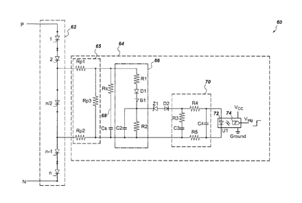
[0023] FIG. 3 shows a schematic diagram 60 of an electronic valve 62 with
over-
voltage detection circuit 64. The electronic valve 62 is connected across
terminals P-N to
bypass any other circuit connected across terminals P-N in the event of an
over-voltage.
The electronic valve 62 includes series connection of semiconductor devices
such as
thyristors. In one embodiment, where there are ii semiconductor devices in
electronic
valve 62, the over-voltage detection circuit 64 is connected across the
semiconductor
device which is at the center, namely n/2, n12+1 or (17 1)12. However, it
should be noted
that this is just an example and in other embodiments, the over-voltage
detection circuit
may be connected across other semiconductor devices.
[0024] Over-voltage detection Circuit 64 includes a voltage divider
circuit 65
formed from resistors Rp1, Rp2 and Rp3 and provides a representative low
voltage across
a break-over diode B1 in a BOD branch 66. The representative low voltage is a
representative of voltage across the semiconductor device to which circuit 64
is
connected. The representative low voltage is significantly lower than the
voltage across
the semiconductor device to which circuit 64 is connected. For example, in one
7
CA 02908909 2015-10-15
273876
embodiment, if the voltage across terminals P-N is 50 kV and there are total 5
series
connected semiconductor devices in electronic valve 62 then the voltage across
each
semiconductor device may be about 10 kV. Furthermore, the representative low
voltage
then may further be reduced to 10 V, as an example. Depending on resistances
of
resistors Rpl, Rp2, Rp3, R1 and R2, the representative low voltage will
change. Thus,
low voltage rating components such as a low voltage BOD can be used in the
circuit 64.
Furthermore, any isolation requirement for the circuit can be designed as in
normal low
voltage circuits/systems, which is the one of the advantage of the present
technique. In
one embodiment, resistance of resistors Rpl and Rp2 is equal and is much
larger than
that of resistor Rp3. Since the power consumption of the resistors Rpl and Rp2
may be
comparatively high, in one embodiment, resistors Rpl and Rp2 may be either
mounted on
a heat-sink or on a separate printed circuit board.
[0025] Over-
voltage detection circuit 64 also includes a break-over diode branch
66 having the break-over diode B1, current limiting resistors R1, R2 and
another diode
D1 which are all connected in series and further a capacitor C2 in parallel
with resistor
R2. Diode D1 protects the break-over diode B1 against excessive reverse
voltage. BOD
branch 66 receives the representative low voltage from the voltage divider
circuit formed
by resistors Rp1, Rp2 and Rp3 and detects an over-voltage condition across the
semiconductor device if the representative low voltage across break-over diode
B1
exceeds a threshold value. In one embodiment, the threshold value is
determined based
on system requirements. For example, assume the rated voltage across terminals
P-N is
50 kV and the maximum voltage the circuit connected across terminals P-N can
withstand is 55 kV. In this case, assuming five semiconductor devices, maximum
voltage
each semiconductor device can withstand is 11 kV. Furthermore, the
representative low
voltage limit, assuming a ratio of 1000:1, would be 10V. Thus, the threshold
value can
then be determined based on resistances of resistors R1, R2 and the
representative low
voltage limit.
8
CA 02908909 2015-10-15
273876
[0026] In one embodiment, capacitor C2 and resistor R2 form a low-pass
filter
which along with diode D1 blocks a displacement current of diode B1 at a
positive dV/dt
rate. In one embodiment, diode D1 is chosen to have fast recovery
characteristics so as to
protect against a reverse voltage across break-over diode B1. Circuit 64
further includes
a snubber circuit 68 having resistor Rs and capacitor Cs to filter out high
frequency
noises. Snubber circuit 68 is connected in parallel with the BOD branch 66.
[0027] In one embodiment, break-over diode branch 66 provides a current to
an
optocoupler U1, when the over-voltage is detected. In other words, when the
voltage
across break-over diode B1 exceeds a threshold value, it starts conducting,
creates a
voltage across resistor R2 and provides a current to optocoupler Ul.
Optocoupler Ul
then sends simultaneous signals to all self-powered gate drive circuits so
that to trigger
synchronized conduction of all semiconductor devices and short circuit
terminals P-N
which results in bypass of any power circuit connected across terminals P-N.
Optocoupler U1 includes a light emitting diode 72 and a phototransistor 74.
The
optocoupler U1 is designed to work as voltage isolation between high-voltage
bypass
inputs and logic controller circuit which is usually at low voltage potential
to ground. In
one embodiment, optocoupler U1 has less than 200 ns propagation delay time and
low
input current. In addition, high performance of common mode noise rejection is
preferable on optocoupler 111.
[0028] Circuit 64 also includes a filtering network 70 comprising
resistors R3,
R4, R5 and capacitors C4, C3 to drive optocoupler U1. Circuit 64 also includes
a zener
diode ZI and a diode D2 connected in between filtering network 70 and BOD
branch 66.
Zener diode Z1 provides an onset voltage at which the filtering network 70
starts to
operate, which helps to prevent faulty triggering of optocoupler U1 and also
ensures that
the filtering network 70 operates at same initial state before any occurrence
of any over-
voltage condition. Diode D2 is a fast recovery diode (optionally) to protect
against the
reverse voltage.
9
CA 02908909 2015-10-15
273876
[0029] When the over-voltage pulse above the threshold value gets applied
to the
BOD B1, i.e. a BOD breakdown voltage, avalanche generation starts in BOD Bl,
providing a current (breakdown current) to charge capacitor C2 and then
trigger the
optocoupler U1. The component R2, C2 and D2 determine the waveform of the
optocoupler LED current, resulting in a slightly delayed turn-on of the
optocoupler. The
output of optocoupler (Vtrig pulse as shown in Figure 3) changes to a high
level from a
low level once an over-voltage is detected by BOD B1. The BOD current quickly
goes
below its holding current, after triggering all semiconductor devices, the BOD
B1 will
then turn off due to its current shunted by the semiconductor device to which
the circuit
64 is connected. Usually the pulsewidth of Vtrig pulse could be several
microseconds.
Therefore, a latch circuit (e.g. D flip-flop) may be needed for saving the
state of over-
voltage detection until it is reset by an upstream controller after faults are
coped with
properly.
[0030] It should be noted that since all semiconductor devices will be
triggered by
a single pulse or signal Vtrig, the signal Vtrig may need to be duplicated and
a multi-
channel trigger signal for semiconductor devices may be generated. The multi-
channel
trigger signal can be a fiber signal generated by a fiber transmitter; or an
electrical signal
generated by isolated pulse transformers with multiple secondary windings,
while its
primary winding is driven by the amplified signal Vtrig. In one embodiment, a
reinforced isolation barrier may be added between primary winding and
secondary
windings to meet high-voltage isolation requirement. In another embodiment,
the control
power for the function circuits i.e., pulse transformers etc. can be taken
from self-
powered gate drive and regulated locally.
[0031] FIG. 4 shows a schematic diagram of a self-powered gate drive
circuit 80
in accordance with an embodiment of the present technique. The Self powered
gate drive
circuit includes a gate drive circuit 82 with a power generation circuit 83.
As discussed
earlier, gate drive circuit 82 triggers a semiconductor device 84 when an over-
voltage is
detected by over-voltage detection circuit 64. Gate drive circuit 82 has been
shown to
CA 02908909 2015-10-15
273876
have a voltage Vcc which is obtained from power generation circuit 83 which
generates
the voltage Vcc from 2 energy storage elements, a super capacitor 86 and a
regular
storage capacitor 88. During normal operation or steady state, the voltage
across
semiconductor device is utilized by a ballast resistor 98 to charge the super
capacitor 86
and storage capacitor 88 and to generate voltage Vcc and derive a gating
energy, i.e., the
energy required to turn on the semiconductor device 84. In one embodiment,
ballast
resistor 98 is very large and charges capacitors 86 and 88 over much longer
time with a
very small current during steady state. In another embodiment, a hybrid energy
recovery
scheme may be used. In this scheme, along with ballast resistor, the gating
energy may
also be derived from a snubber circuit 90 at a steady state as well as a
transient state.
During the steady state the energy is transferred from high anode potential
(usually
>3kV) to cathode-referenced potential of semiconductor device 84 and during
the
transient state, some transient alternating current may charge the snubber
capacitor which
then can transfer the energy to capacitors 86 and 88. The energy recovery
scheme uses a
capacitive divider formed by the snubber capacitor and the super capacitor or
storage
capacitor to recover charge during transits as well as the ballast resistor to
charge the
super capacitor over much large time period at steady state. The voltage of
power
generation circuit 83 is clamped to a low voltage level Vcc, for example 30
Vdc by a
voltage damper 92. Two block diodes 94 and 96 block a reverse current from
capacitors
86 and 88 respectively. This is needed because when semiconductor switch 84 is
conducting, it will bypass the power generation circuit 84 and thus, the block
diodes 94
and 96 will protect the capacitors 86 and 88 from discharging. The snubber
current will
be bypassed by a power electronic switch 100 (such as MOSFET) controlled by
voltage
damper 92 once the super capacitor 86 and storage capacitor 88 are fully
charged to the
pre-determined level of voltage Vcc. In one embodiment, voltage damper 92 may
be
built by using a device with characteristics of zener diodes.
[0032] One of the
advantages of the present technique is it needs no processors
and precise analog circuits which complicate the design and reduce
reliability.
Furthermore, the over-voltage detection is conducted by break-over diode which
is robust
11
CA 02908909 2015-10-15
273876
and insensitive to noises. The over-voltage trigger level can be precisely set
by selecting
break-over diode with associate break over-voltage in a wide variety of low-
voltage BOD
family, which results in noise-insensitive over-voltage detection, high
repeatability of
bypass performance and accuracy of over-voltage protection. Another advantage
of the
present technique is that turn-on of bypass semiconductor devices can be
synchronized
due to the same triggering signal being sent to all bypass semiconductor
devices
simultaneously. This would
lead to little voltage unbalance on each bypass
semiconductor device during transients and highly improve the reliability of
overall
bypass device. Furthermore, the mechanical circuit breaker will be controlled
to close in
coordination with semiconductor devices.
[0033] While there
have been described herein what are considered to be
preferred and exemplary embodiments of the present invention, other
modifications of
these embodiments falling within the scope of the invention described herein
shall be
apparent to those skilled in the art.
12