Note: Descriptions are shown in the official language in which they were submitted.
81792129
DRIVE OUTPUT HARMONIC MITIGATION DEVICES AND METHODS 01? USE
THEREOF
Field
The present invention relates to conditioning of an electrical power signal,
and
morc particularly, to apparatus and methods for reshaping an electrical power
output waveform
generated by a first device and presenting the altered waveform to another
device or circuit.
Packgrourtcl
Circuits for altering electrical power waveforms are known. For example, L-R-C
(inductor-resistor-capacitor) low pass filters and sine wave filters are known
for use in altering
a power output from a variable speed drive for an electric motor, e.g., for
conditioning a pulse
width modulated output in order to supply the motor with a more sinusoidal
power waveform.
Notwithstanding, improved and/or alternative power conditioning circuits
remain desirable.
CA 2909163 2018-12-03
CA 02909163 2015-10-08
WO 2014/169053 PCT/US2014/033523
Summary
The disclosed subject matter relates to a device for modifying an input
electrical
waveform generated by a source of electrical power provided on a first
conductor. The device
includes a first inductor capable of connecting to the first conductor. A
second inductor is
connected in series to the first inductor distal to the first conductor and a
capacitor is connected
in series with the second inductor distal to the first inductor. A second
conductor is connected
between the first inductor and the second inductor, the second conductor
capable of presenting
an output waveform.
In another embodiment of the present disclosure, a relative polarity between
the
first inductor and the second inductor is additive.
In another embodiment of the present disclosure, the input electrical waveform
is
a first electrical waveform and wherein the source of electrical power
produces a plurality of
electrical waveforms, each provided on one of a plurality of conductors and
further comprising a
plurality of devices, each having a first inductor capable of connecting to
one of the plurality of
conductors, a second inductor connected in series to the first inductor, a
capacitor connected in
series with the second inductor distal to the first inductor and a plurality
of second conductors
connected between the first inductor and the second inductor, the plurality of
second conductors
capable of presenting a multi-phase output waveform.
In another embodiment of the present disclosure, the plurality of electrical
waveforms is three in number, each having a different phase to provide three-
phase electrical
power at three second conductors.
In another embodiment of the present disclosure, the first inductor and the
second
inductor are disposed on a common core.
In another embodiment of the present disclosure, each of the series connected
first
2
CA 02909163 2015-10-08
WO 2014/169053 PCT/US2014/033523
inductors and second inductors are disposed on a common core.
In another embodiment of the present disclosure, the source of electrical
power is
an adjustable speed drive.
In another embodiment of the present disclosure, the source of electrical
power
produces the input electrical waveform by pulse-width modulation.
In another embodiment of the present disclosure, the output waveform is
supplied
to an electric motor.
In another embodiment of the present disclosure, the device reduces harmonic
currents otherwise present absent the second inductor.
In another embodiment of the present disclosure, a resistor is interposed
between
and in series with the second inductor and the capacitor.
In another embodiment of the present disclosure, at least one of the first and
second inductors is an adaptive passive inductor.
In another embodiment of the present disclosure, each of the first and second
inductors is an adaptive passive inductor.
In another embodiment of the present disclosure, the device has an E-shaped
core,
each of the first and second inductors being wound about a corresponding leg
of the E-shaped
core and further comprising an I-shaped core disposed proximate the ends of
each leg of the E-
shaped core and further comprising a high permeability core gap piece disposed
between each
leg of the E-shaped core and the I-shaped core.
In another embodiment of the present disclosure, a filter for filtering an
input
electrical power waveform produces an output power waveform. The filter has an
inductor
having first and second coils and a capacitor connected in series. The filter
has a tap terminal
intermediate the first and second inductors. A conductor extends from the tap
terminal and is
3
81792129
capable of being connected to a load.
In another embodiment of the present disclosure, the input electrical power is
provided by an adjustable speed drive and the load is a motor.
In another embodiment of the present disclosure, the inductor is of the
passive
adaptive type and further comprising a resistor connected in series between
the inductor and the
capacitor.
In another embodiment of the present disclosure, a filter for filtering a
three-phase
electrical power waveform produces a three-phase output power waveform. The
filter has an
inductor having three sets of first and second coils, each having a capacitor
connected in series
therewith. Each of the capacitors are connected in common distal to the series
connection with
the second coil. Each of the three sets of first and second inductors having a
tap intermediate the
first and second inductors where the output waveform is present, each tap
capable of being
connected to a load.
In another embodiment of the present disclosure, the inductor is passive
adaptive
and further comprising a resistor connected in series between the inductor and
the capacitor, the
load being a three-phase electric motor.
In another embodiment of the present disclosure, the inductor is formed on an
E-
shaped core each of the three sets of coils being wound on a corresponding leg
of the E shape.
In another embodiment of the present disclosure, the device has a three phase
core, each of the first and second inductors being wound about a corresponding
portion of the
three phase core.
4
CA 2909163 2018-12-03
81792129
According to one aspect of the present invention, there is provided a device,
comprising: a common core; a first inductor, wherein the first inductor is
comprised of a first
plurality of magnetically coupled coils; a second inductor, wherein the second
inductor is
comprised of a second plurality of magnetically coupled coils; wherein the
second inductor is
.. connected in series by a plurality of connections to the first inductor;
wherein the plurality of
connections is capable of presenting at least one output waveform; and wherein
the first
inductor and the second inductor are disposed on the common core so that the
first plurality of
coils and the second plurality of coils are all magnetically coupled and
disposed on the
common core.
Brief Description of the Drawings
For a more complete understanding of the present disclosure, reference is made
to
4a
CA 2909163 2018-12-03
CA 02909163 2015-10-08
WO 2014/169053 PCT/US2014/033523
the following detailed description of exemplary embodiments considered in
conjunction with the
accompanying drawings.
FIG. l is circuit diagram of a prior art sine wave filter.
FIG. 2 is a circuit diagram of a sine wave filter in accordance with a first
embodiment of the present disclosure.
FIG. 3 is a schematic circuit diagram of an inductor that may be used with a
sine
wave filter in accordance with another embodiment of the present disclosure.
FIG. 4 is a circuit diagram of a sine wave filter in accordance with another
embodiment of the present disclosure.
FIG. 5 is a graph of frequency response for a sine wave filter in accordance
with
an embodiment of the present disclosure compared to a prior art filter.
FIG. 6 is a rear perspective view of a sine wave filter in accordance with an
embodiment of the present disclosure.
FIG. 7 is a front perspective view of a sine wave filter in accordance with an
embodiment of the present disclosure.
Detailed Description of Exemplary Embodiments
An aspect of the present disclosure is the use of the apparatus disclosed
herein for
drive output filters that provide a nearly sinusoidal output voltage when
driven from variable
frequency drives or other types of Pulse-width modulation (PWM) inverters with
switching
frequencies from 2kHz to 8kHz. In some embodiments, the apparatus of the
present disclosure
are utilized to eliminate and/or minimize the problem of motor/cable
insulation failures, heating,
and/or audible noise. In some embodiments, the apparatus disclosed by the
present disclosure are
utilized to reduce electromagnetic interference (EMI) by eliminating the high
dV/dt associated
5
CA 02909163 2015-10-08
WO 2014/169053 PCT/US2014/033523
with inverter output waveforms. In some embodiments, added cable protection
and the economy
of using standard grade electrical wire is a significant benefit of using the
sine wave filters of the
present disclosure to protect against long lead drive-to-motor excess voltage
problems.
FIG. 1 shows a prior art L-R-C (inductor-resistor-capacitor) low pass drive
output
filter F. Such filters may also be known as Sine wave filters. Prior art Sine
wave filters may
shunt a high PWM switching frequency (typically 2 kHz to 8 kHz), e.g., from an
adjustable
speed drive (ASD) through capacitors Cl, C2, C3 and provides primarily just
the fundamental
voltage waveform to a motor (typically 10 or 120 Hz). In some instances, a
three phase inductor
I is tuned with a capacitor(s) Cl, C2, C3 below the drive switching frequency.
In some
instances, a resistor or resistors R1, R2, R3 may be used to provide damping,
to increase filter
stability and reduce the initial inrush of current to the filter F when the
drive ASD is first turned
on. An aspect of the present disclosure is the recognition that prior art
approaches may employ a
trade-off between inductor size and capacitance value. More particularly,
because the inductor is
made from copper windings, it is typically the most expensive part of the
filter. As a result, there
is an incentive to reduce the size of the inductor, but this has the
undesirable effect of lowering
its inductance. To compensate for the lowered inductance, the capacitance
value of the capacitor
is increased to maintain the same low pass filter cutoff frequency. This can
result in an increase
in the harmonic currents through the inductor and the capacitor. Increases in
harmonic current
increase power losses within the inductor, with the electrical power being
converted to waste
heat and mechanical vibration. The increased winding losses in the inductor
conductors may be
due to proximity effects, gap heating, and skin effect heating associated with
increased harmonic
current. These factors represent a limitation on the reduction of inductor
size, in that the inductor
size may need to be maintained at a certain minimum to reduce the flux density
in the core to
reduce power losses to an acceptable level or a more expensive, lower loss
core material may
6
81792129
need to be used.
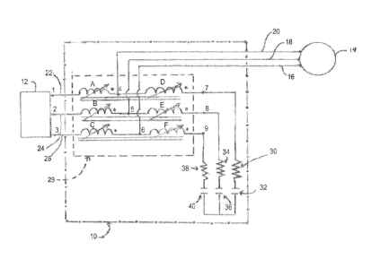
FIG. 2 shows a filter 10 in accordance with. an embodiment of the present
disclosure interposed between an adjustable speed drive ASD 12 and a motor 14.
The ASD 12
would receive electrical power from, e.g., a power grid or a generator (not
shown). The motor
14 has a three phase input as indicated by lines 16, 18,20 and the ASD has a
three phase output,
as indicated by lines 22,24, 26. An inductor 28 intermediates between the ASD
12 and the
motor 14. The inductor 28 may be of the passive adaptive type, as shown in
FIG. 3 below. The
filter 10, may permit reducing inductor size, while avoiding the above-
mentioned issues
pertaining to winding losses, harmonic currents, etc., outlined above
associated with reducing the
size of the typical L-R-C filter. This greater latitude in reducing inductor
28 size is due in part to
the arrangement of the coils A, B, C, D, E, F and the connections of the motor
lines 16, 18, 20 to
tap terminals 4, 5, 6 intermediate windings A and D, B and E and C and F,
respectively. The
inductor 28 is coupled to the ASD at terminals 1,2 and 3 and has a plurality
of windings A, B, C,
D, E, F, each of which have a variable inductance attributable to the inductor
28 being of a
passive adaptive type. Terminals 7, 8, 9 at the end of windings D, E, and F,
respectively,
connect to resister-capacitor couples 30 and 32, 34 and 36 and 38 and 40,
respectively. The
polarity of windings A, B, C with respect to D, E, F are shown by a dot.
FIG. 3 shows an inductor 128 that may be utilized in filter 10 of FIG. 2. The
inductor 128 has an E-shaped core 142 and an I-shaped core element 144, both
of which may be
.. made from core steel. The windings A and D, B and E and C and F are
disposed around the
three arms 142A, 142B and 142C of the E-shaped core 142, respectively. The
terminals 1-9
referred to above in FIG. 2 are also shown in FIG. 3. High permeability core
gap pieces,
"PAPS" 146A, 146B, 146C, as described in U.S. Patent Publication No.
20120256719, entitled
"Harmonic Mitigation Devices and Applications Thereof,"
7
CA 2909163 2018-12-03
81792129
may be interposed between each of the arms
142A, 142B, 142C and the I-shaped element 144. The FAPS have the effect of
providing
adaptive passive inductance as indicated by the arrow symbols on the coils A,
B, C, D, E, F in
FIG. 2. When an inductor, like inductor 128 of FIG. 3, is used in the filter
10 of FIG. 2,
windings A, B and C are coupled to windings D, E and F with the polarities
indicated in FIG. 2
to increase the inductance tuned with the capacitor. In the embodiment of FIG.
2, the capacitors
32, 36,40 will only need to be rated for a reduced current as compared to the
typical filter (See
FIG. 1) with just three coils, e.g., A, B and C. In some embodiments, the D, E
and F windings
only need to be rated for the capacitor current opposed to the A, B and C
windings which have to
be rated for the full motor current. In some embodiments, the D, E and F
windings add relatively
minor cost and size to the filter 10. In some embodiments, the voltage
insertion loss of the filter
is also reduced since only windings A, B and C are in series with the motor 14
and not windings
D, E and F. While the inductor 28, 128 of FIG. 3 shows a variable inductance
by coils A, B, C,
D, E, F, attributable to the use of FAPS, an inductor made without FAPS, such
as described in
U.S Patent No. 7,142,081 may be used for some applications. The inductor 28,
128 may have a
three phase configuration other than an El configuration as described above
relative to FIG. 3.
For example, the inductor 28, 128 may have multiple gaps per leg.
Some embodiments, e.g., as illustrated by filter 10 of FIG. 2, may require
damping e.g., by resistors 30, 34, 38 to reduce inrush when the filter 10 is
first energized to
reduce ringing near the resonant frequency of the filter 10 during operation.
Alternatively, in
some applications, the filter 10 may not require additional damping. FIG. 4
shows a filter 210 in
accordance with an embodiment of the present disclosure without damping
resistors like 30, 34,
38 or the adaptive passive inductor 28 utilized in the embodiment of FIG. 2.
The inductor 228 of
Fig. 4 is similar to the one shown in FIGS. 2 and 3 but without the FAPS. The
arrangement of
8
CA 2909163 2018-12-03
CA 02909163 2015-10-08
WO 2014/169053 PCT/US2014/033523
the coils A, B, C, D, E, F and the connections of the motor lines 216, 218,
220 to tap terminals
4, 5, 6 intermediate windings A and D, B and E and C and F, respectively, is
the same as in
FIGS. 2 and 3. The inductor 228 is coupled to the ASD 212 at terminals 1,2 and
3. Each
individual coil, D, E, and F, displays self-inductance and additional, mutual
inductances from the
other five coils and may each be tuned with the capacitors 250, 252, 254,
respectively, to the
switching frequency of the ASD drive 212.
FIG. 5 shows the difference in frequency response between a prior art drive
output filter, e.g., as shown in FIG. 1 and the filter 210 shown in FIG. 4.
FIG. 5 shows that the
prior art filter F exhibits a gradual response, whereas the filter 210
exhibits an optimal
attenuation at a specific frequency, in the example shown in FIG. 4a, 2 kHz.
FIGS. 6 and 7 show a filter 310 in accordance with an embodiment of the
present
disclosure where additional damping by resistors is omitted consistent with
the circuit shown in
FIG. 4. The A, B and C windings of the filter 310 may be constructed from
multiple turns, e.g.,
twelve, of insulated 7.5" x 0.035" copper sheet. The D, E and F windings of
the filter 310 may
be wound with, e.g., four turns of biflar 0.102"x 0.204" magnet wires. In one
embodiment, the
filter 310 may be used as a filter for a 480 V motor rated at 415 A, which is
connected to the
filter 310 via lines 316, 318, 320. The present invention is explained with
reference to the
attached drawings, wherein like structures are referred to by like numerals
throughout the several
views. The drawings shown are not necessarily to scale, with emphasis instead
generally being
placed upon illustrating the principles of the present invention. Further,
some features may be
exaggerated to show details of particular components.
The figures constitute a part of this specification, include illustrative
embodiments
of the present invention and illustrate various objects and features thereof.
Further, the figures
are not necessarily to scale, in that some features may be exaggerated to show
details of
9
CA 02909163 2015-10-08
WO 2014/169053 PCT/US2014/033523
particular components. In addition, any measurements, specifications and the
like shown in the
figures are intended to be illustrative, and not restrictive. Therefore,
specific structural and
functional details disclosed herein are not to be interpreted as limiting, but
merely as a
representative basis for teaching one skilled in the art to variously employ
the present invention.
Detailed embodiments of the present invention are disclosed herein, however,
it is
to be understood that the disclosed embodiments are merely illustrative of the
invention that may
be embodied in various forms. In addition, each of the examples given in
connection with the
various embodiments of the invention are intended to be illustrative, and not
restrictive. Any
alterations and further modifications of the inventive feature illustrated
herein, and any
additional applications of the principles of the invention as illustrated
herein, which would
normally occur to one skilled in the relevant art and having possession of
this disclosure, are to
be considered within the scope of the invention.
Throughout the specification and claims, the following terms take the meanings
explicitly associated herein, unless the context clearly dictates otherwise.
The phrases "an
embodiment" and "in some embodiments" as used herein do not necessarily refer
to the same
embodiment(s), though it may. Furthermore, the phrases "another embodiment"
and "in some
other embodiments" if used herein, do not necessarily refer to a different
embodiment, although
it may. Various embodiments of the invention may be readily combined, without
departing from
the scope or spirit of the invention.
In addition, as used herein, the term "or" is an inclusive "or" operator, and
is
equivalent to the term "and/or," unless the context clearly dictates
otherwise. In addition,
throughout the specification, the meaning of "a," "an," and "the" include
plural references. The
meaning of "in" includes "in" and "on."
It will be understood that the embodiments described herein are merely
exemplary
CA 02909163 2015-10-08
WO 2014/169053 PCT/US2014/033523
and that a person skilled in the art may make many variations and
modifications without
departing from the spirit and scope of the claimed subject matter. For
example, while an
iron/steel core is shown for coils A, B, C, D, E, F in FIGS. 2-4, a ferrite
core could be used. All
such variations and modifications are intended to be included within the scope
of the appended
claims.
11