Note: Descriptions are shown in the official language in which they were submitted.
CA 02909552 2015-10-14
WO 2014/179343 PCT/US2014/035926
SYSTEMS, DEVICES, AND METHODS FOR ENERGY EFFICIENT ELECTRICAL
DEVICE ACTIVATION
FIELD
[00 1] The subject matter described herein relates generally to changing
the state of power
consumption of an electrical device in an efficient manner, for example,
within an analyte
monitoring environment.
BACKGROUND
[002] The detection and/or monitoring of analyte levels, such as glucose,
ketones, lactate,
oxygen, hemoglobin Al C, or the like, can be vitally important to the health
of an individual
having diabetes. Diabetics generally monitor their glucose levels to ensure
that they are being
maintained within a clinically safe range, and may also use this information
to determine if
and/or when insulin is needed to reduce glucose levels in their bodies or when
additional glucose
is needed to raise the level of glucose in their bodies.
[003] Growing clinical data demonstrates a strong correlation between the
frequency of
glucose monitoring and glycemic control. Despite such correlation, many
individuals diagnosed
with a diabetic condition do not monitor their glucose levels as frequently as
they should due to a
combination of factors including convenience, testing discretion, pain
associated with glucose
testing, and cost. For these and other reasons, needs exist for improved
analyte monitoring
systems, devices, and methods.
SUMMARY
[004] A number of systems have been developed for the automatic monitoring
of the
analyte(s), like glucose, in a bodily fluid of a user, such as in the blood,
interstitial fluid ("ISF"),
dermal fluid, or in other biological fluid. Some of these systems include a
sensor that can be at
- 1 -
CA 02909552 2015-10-14
WO 2014/179343 PCT/US2014/035926
least partially positioned "in vivo" within the user, e.g., transcutaneously,
subcutaneously, or
dermally, to make contact with the user's bodily fluid and sense the analyte
levels contained
therein. These systems are thus referred to as in vivo analyte monitoring
systems.
[005] The sensor is generally part of a sensor control device that resides
on (or in) the body
of the user and contains the electronics and power source that enable and
control the analyte
sensing. The sensor control device, and variations thereof, can be referred to
as a "sensor control
unit," an "on-body electronics" device or unit, an "on-body" device or unit,
or a "sensor data
communication" device or unit, to name a few.
[006] The analyte data sensed with the sensor control device can be
communicated to a
separate device that can process and/or display that sensed analyte data to
the user in any number
of forms. This device, and variations thereof, can be referred to as a "reader
device" (or simply a
"reader"), "handheld electronics" (or a handheld), a "portable data
processing" device or unit, a
"data receiver," a "receiver" device or unit (or simply a receiver), or a
"remote" device or unit, to
name a few. The reader device can be a dedicated use device, a smart phone, a
tablet, a wearable
electronic device such as a smart glass device, or others.
[007] In vivo analyte monitoring systems can be broadly classified based on
the manner in
which data is communicated between the reader device and the sensor control
device. One type
of in vivo system is a "Continuous Analyte Monitoring" system (or "Continuous
Glucose
Monitoring" system), where data can be broadcast from the sensor control
device to the reader
device continuously without prompting, e.g., in an automatic fashion according
to a broadcast
schedule. Another type of in vivo system is a "Flash Analyte Monitoring"
system (or "Flash
Glucose Monitoring" system or simply "Flash" system), where data can be
transferred from the
- 2 -
CA 02909552 2015-10-14
WO 2014/179343 PCT/US2014/035926
sensor control device in response to a scan or request for data by the reader
device, such as with
a Near Field Communication (NFC) or Radio Frequency Identification (RFID)
protocol.
[008] Provided herein are a number of example embodiments of systems,
devices, and
methods that allow the state (or mode) of power consumption for a device, such
as a sensor
control device, to be changed in an energy efficient manner. Changing of the
state of power
consumption can include, for example, changing from a low power state (e.g.,
powered off) to a
higher power state (e.g., powered on). In some cases, this change of state is
referred to as
"activation" and is employed, for example, when a sensor control device is
first put in use by a
wearer. For ease of illustration, many of the embodiments described herein
will refer to
changing the power state of a sensor control device, although these
embodiments are not limited
to such.
[009] In certain embodiments an activation sensor is provided with the
sensor control
device and operation of the activation sensor causes activation of the
internal electronics. The
activation sensor can be an optical activation sensor that produces a response
when exposed to
ambient optical light or another light source. The exposure to light (or some
other trigger such as
a magnetic field) and subsequent activation can be accomplished before
applying the device to
the body of a user, for example, during the unpacking of the applicator
assembly. The optical
activation sensor can be part of an activation circuit for the sensor control
device. Upon
exposure to light, the optical activation sensor, which may be in the form of
an optically
activatable switch, can cause the activation circuit to initiate an on-board
processor. The
processor, in turn, can maintain the internal electronics in the active state
during the duration of
use of the sensor control device, or during the lifetime of the device's power
supply.
Verification of the initiation of the electronics can be performed by the user
or automatically by
-3 -
CA 02909552 2015-10-14
WO 2014/179343 PCT/US2014/035926
the system, such as by generation of a message or other indication to the user
at the reader
device. Also provided are methods of manufacturing the sensor control device
with a sensor
control activation sensor such as an optical sensor.
[010] In other embodiments, the sensor control device is capable of
utilizing transmissions
over a wireless communication protocol to change a power state, or to
recognize when such a
change should be effected.
[011] For example, the sensor control device can be capable of sending and
receiving
communications according to a Bluetooth Low Energy (BTLE) protocol. In certain
embodiments, the sensor control device, while operating in a first power state
(e.g., a low power
state such as a powered-off or inactivated state, a storage state, or a sleep
state), can receive such
a wireless communication from the reader device and recognize that it is or is
part of a BTLE
advertising sequence (or is a single advertising message). The recognition can
be made either
through hardware or software. Upon making that recognition, the sensor control
device can
change to a second, higher power state (e.g., a state of greater power
consumption than the first
power state, such as a powered-on or activated state, or an awake state). In
certain embodiments,
the sensor control device can recognize the advertising sequence without first
demodulating the
communication.
[012] In some embodiments the sensor control device receives a second or
subsequent
advertising sequence from the reader device when in the second power state.
The sensor control
device can demodulate the second advertising sequence and determine if it
contains an activation
request message and, if so, then transmit a confirmation response to the
reader device. If the
demodulated communication does not contain the activation request message,
then the state of
the sensor control device can be changed back to the first power state. In
some embodiments,
- 4 -
CA 02909552 2015-10-14
WO 2014/179343 PCT/US2014/035926
the first power mode is a sleep (or storage) mode and the second power mode is
a normal
operation mode.
[013] A number of variations to the aforementioned embodiments are also
provided. For
example, the advertising sequence can include a series of advertising packets
transmitted at a
predetermined time interval. The advertising sequence can include a
connectable directed
advertising packet type, a connectable undirected advertising packet type, a
non-connectable
undirected advertising packet type, or a scannable undirected advertising
packet type, each of
which can be the activation request message.
[014] In still other embodiments, successive radio frequency (RF)
communications can be
used to supply power to, for example, the sensor control device. The sensor
control device can
be in a low-power state (e.g., a power-off or inactivated mode, a storage
mode, or a sleep mode)
where full operating power is not being supplied. The sensor control device
can utilize the
power of the received wireless communications to cause a local power source to
begin supplying
the operating power, thereby transitioning the sensor control device to a
higher-power state (e.g.,
a normal, awake, or activated operating state). In many of these embodiments,
the wireless
communications are sent and received in accordance with a Near Field
Communication (NFC)
protocol, although other protocols can be used as well.
[015] Adaptive embodiments are also described where the power mode of the
sensor
control device is directly or indirectly monitored by the reader device and
one or more of the
number, type, interval, or power of the successive wireless communications is
adjusted by the
reader device until sufficient power is supplied to enable the sensor control
device to transition to
a higher-power mode. The embodiments described herein are particularly
suitable when the
reader device is in the form of a smartphone.
-5 -
CA 02909552 2015-10-14
WO 2014/179343 PCT/US2014/035926
[016] Other systems, devices, methods, features and advantages of the
subject matter
described herein will be or will become apparent to one with skill in the art
upon examination of
the following figures and detailed description. It is intended that all such
additional systems,
devices, methods, features and advantages be included within this description,
be within the
scope of the subject matter described herein, and be protected by the
accompanying claims. In
no way should the features of the example embodiments be construed as limiting
the appended
claims, absent express recitation of those features in the claims.
BRIEF DESCRIPTION OF THE FIGURES
[017] The details of the subject matter set forth herein, both as to its
structure and operation,
may be apparent by study of the accompanying figures, in which like reference
numerals refer to
like parts. The components in the figures are not necessarily to scale,
emphasis instead being
placed upon illustrating the principles of the subject matter. Moreover, all
illustrations are
intended to convey concepts, where relative sizes, shapes and other detailed
attributes may be
illustrated schematically rather than literally or precisely.
[018] FIG. 1 is a high level diagram depicting an example embodiment of an
analyte
monitoring system for real time analyte (e.g., glucose) measurement, data
acquisition and/or
processing.
[019] FIG. 2A is a block diagram depicting an example embodiment of a
reader device
configured as a smartphone.
[020] FIGs. 2B-C are block diagrams depicting example embodiments of a
sensor control
device.
[021] FIG. 3 is a block schematic view depicting an example embodiment of
sensor
electronics having an optically-based activation circuit.
- 6 -
CA 02909552 2015-10-14
WO 2014/179343 PCT/US2014/035926
[022] FIG. 4 is a flowchart depicting an example embodiment of a method of
using the
analyte monitoring system with an optical sensor.
[023] FIGs. 5A-I are illustrations of the steps in performing an example
embodiment of a
method of using the analyte monitoring system with an optical sensor.
[024] FIG. 6A is an exploded view of an example embodiment of an
applicator.
[025] FIG. 6B is an exploded view of an example embodiment of a container
for a sensor
assembly.
[026] FIG. 7 is a block schematic view depicting an example embodiment of
sensor
electronics having a magnetically-based activation circuit.
[027] FIG. 8 is a flowchart depicting an example embodiment of a method of
using the
analyte monitoring system with a magnetic sensor.
[028] FIGs. 9A-D are construction views of a sensor control device
subassembly.
[029] FIG. 9E is a perspective view of a complete sensor electronics
subassembly.
[030] FIGs. 10A-D illustrate the process of co-molding/overmolding the
embodiment of
FIG. 9E.
[031] FIGs. 11A-C are assembly and sectional views of an alternative snap-
together
embodiment for the assembly of FIG. 9E.
[032] FIGs. 12A-C are assembly views illustrating adhesive backing
application in
producing a final sensor control device ready for use.
[033] FIGs. 13-14 are block diagrams depicting example embodiments of
methods for
establishing communication between a sensor control device and a reader
device.
[034] FIG. 15 is a block diagram depicting another example embodiment of a
sensor control
device.
- 7 -
CA 02909552 2015-10-14
WO 2014/179343 PCT/US2014/035926
[035] FIG. 16 is a block diagram depicting an example embodiment of power
management
circuitry.
[036] FIGs. 17A-B are flow diagrams depicting an example embodiment of a
method of
supply power to a sensor control device with successive RF communications sent
by a reader
device.
[037] FIG. 18 is a conceptual timing diagram depicting power levels of a
reader device and
sensor control device, and various communications and communication attempts
between those
devices.
[038] FIG. 19 is a flow diagram depicting an example embodiment of a method
of
adaptively supplying power to a sensor control device.
DETAILED DESCRIPTION
[039] The present subject matter is not limited to the particular
embodiments described, as
those are only examples and may, of course, vary. Likewise, the terminology
used herein is for
the purpose of describing particular embodiments only, and is not intended to
be limiting, since
the scope of the present disclosure will be limited only by the appended
claims.
[040] In conventional analyte monitoring systems, the sensor control device
has a small
physical form enabling it to be worn inconspicuously by the user. This
constrains the size of the
device's internal electronics and power source. If the sensor control device
has a limited lifespan
dictated by the long-term reliability of the sensor (e.g., fourteen days),
then it will be disposable
and replaceable with another device. The desirability to minimize the cost of
each device adds
further pressure to minimize the size of the power source and the rate at
which it is used. The
power requirements of the sensor control device electronics and the rate at
which the software
operates those electronics are therefore minimized in the design process.
- 8 -
CA 02909552 2015-10-14
WO 2014/179343 PCT/US2014/035926
[041] To this end, the sensor control device is often shipped and stored in
a low-power
mode where the power source does not supply operating power to all or most of
the sensor
electronics. In some embodiments, only wireless communication circuitry is
active, operating in
a mode that draws minimal quiescent current to listen for an activation RF
signal.
[042] In this low-power mode the power source can be disconnected
mechanically from the
internal electronics (such as by placement of a removable insulator between
the device's contacts
and the power source), electronically (such as with a controllable isolation
circuit) in a manner
that minimizes leakage current from the source, or otherwise. The power source
can be
connected once the wearer is ready to begin use of the sensor.
[043] Many of the embodiments described herein provide techniques for
changing the
power state of a sensor control device with improved efficiency, cost, and
reduced hardware and
software (among others) as compared to conventional techniques.
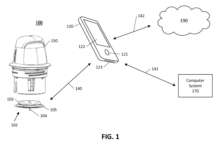
[044] An example embodiment of an in vivo analyte monitoring system 100
with which the
embodiments described herein can be used is depicted in the illustrative view
of FIG. 1. Here,
system 100 includes a sensor control device 102 and a reader device 120 that
can communicate
with each other over a local wireless communication path (or link) 140, which
can be uni-
directional or bi-directional. The communications sent across liffl( 140
contain digital messages
in a frame format (which includes packets) and can be based on a Near Field
Communication
(NFC) protocol (including an RFID protocol), Bluetooth or Bluetooth Low Energy
(BTLE)
protocol, Wi-Fi protocol, proprietary protocol, or others. Reader device 120
is also capable of
wired, wireless, or combined communication over communication paths (or links)
141 and 142
with other systems or devices, such as a computer system 170 (e.g., a server
for a website, a
personal computer, a tablet, and the like) or cloud-based storage 190.
- 9 -
CA 02909552 2015-10-14
WO 2014/179343 PCT/US2014/035926
[045] Any version of Bluetooth can be used for communication links 140,
141, and 142.
One such version is Bluetooth Low Energy (BTLE, BLE), which is also referred
to as Bluetooth
SMART or Bluetooth SMART Ready. A version of BTLE is described in the
Bluetooth
Specification, version 4.0, published June 30, 2010, which is explicitly
incorporated by reference
herein for all purposes. It should be noted that one of ordinary skill in the
art will readily
recognize that the embodiments described herein can be used with subsequent
iterations of the
Bluetooth protocols, or with new protocols that operate in a similar fashion
to the Bluetooth
protocols described herein, regardless of whether those protocols are in
existence as of the time
of this filing.
[046] The use of BTLE communication (or other low-energy wireless
standards), allows for
reduced energy usage, which can be particularly important in performing data
transmissions
between sensor control device 102 and reader device 120 over link 140. This,
in turn, allows for
either reduction of the battery size in sensor control device 102 or extension
of the battery life (or
combinations thereof).
[047] Use of a low-energy wireless communication protocol can allow the
respective
communication interfaces to have, for example, a lower duty cycle (i.e., less
frequent active
operation, which drains less battery power), shorter periods of usage, or any
combination thereof
In addition to BTLE, other wireless protocols such as Wi-Fi, cellular, Zigbee,
and custom
protocols can be used instead of, or in addition to, BTLE for links 140, 141,
and 142. These
other protocols, however, typically require either more energy than BTLE, are
not widely
integrated into smartphones or tablets, or are not approved for worldwide use.
Today and for the
foreseeable future, smartphones, tablets, and other portable computing devices
will be provided
to customers with Bluetooth capability, as that family of protocols is widely
regarded as the most
- 10 -
CA 02909552 2015-10-14
WO 2014/179343 PCT/US2014/035926
convenient to accomplish close proximity communication between, e.g., a
tablet, and the tablet's
peripherals (e.g., wireless headset, mouse, keyboard, etc.).
[048] Other embodiments of sensor control device 102 and reader device 120,
as well as
other components of an in vivo-based analyte monitoring system that are
suitable for use with
the system, device, and method embodiments set forth herein, are described in
US Patent
Application Publ. No. 2011/0213225 (the '225 Publication), which is
incorporated by reference
herein in its entirety for all purposes.
[049] Sensor control device 102 can include a housing 103 containing in
vivo analyte
monitoring circuitry and a power source (shown in FIGs. 2B-C). The in vivo
analyte monitoring
circuitry is electrically coupled with an analyte sensor 104 that extends
through a patch 105 and
projects away from housing 103. An adhesive layer (not shown) can be
positioned at the base of
patch 105 for attachment to a skin surface of the user's body. Other forms of
attachment to the
body may be used, in addition to or instead of adhesive. Sensor 104 is adapted
to be at least
partially inserted into the body of the user, where it can make contact with
the user's bodily fluid
and, once activated, used with the in vivo analyte monitoring circuitry to
measure and collect
analyte-related data of the user. Generally, sensor control device 102 and its
components can be
applied to the body with a mechanical applicator 150 in one or more steps, as
described in the
incorporated '225 Publication, or in any other desired manner.
[050] After activation, sensor control device 102 can wirelessly
communicate the collected
analyte data (such as, for example, data corresponding to monitored analyte
level and/or
monitored temperature data, and/or stored historical analyte related data) to
reader device 120
where, in certain embodiments, it can be algorithmically processed into data
representative of the
- 11 -
CA 02909552 2015-10-14
WO 2014/179343 PCT/US2014/035926
analyte level of the user and then displayed to the user and/or otherwise
incorporated into a
diabetes monitoring regime.
[051] As shown in FIG. 1, reader device 120 includes a display 122 to
output information to
the user and/or to accept an input from the user (e.g., if configured as a
touch screen), and one
optional user interface component 121 (or more), such as a button, actuator,
touch sensitive
switch, capacitive switch, pressure sensitive switch, jog wheel or the like.
Reader device 120
can also include one or more data communication ports 123 for wired data
communication with
external devices such as computer system 170 (described below). Reader device
120 may also
include an in vitro analyte meter, including an in vitro test strip port (not
shown) to receive an in
vitro analyte test strip for performing in vitro analyte measurements.
[052] Computer system 170 can be used by the user or a medical professional
to display
and/or analyze the collected analyte data with an informatics software
program. Computer
system 170 may be a personal computer, a server terminal, a laptop computer, a
tablet, or other
suitable data processing device, and can be (or include) software for data
management and
analysis and communication with the components in analyte monitoring system
100.
[053] The processing of data and the execution of software within system
100 can be
performed by one or more processors of reader device 120, computer system 170,
and/or sensor
control device 102. For example, raw data measured by sensor 104 can be
algorithmically
processed into a value that represents the analyte level and that is readily
suitable for display to
the user, and this can occur in sensor control device 102, or it can occur in
reader device 120 or
computer system 170 after receipt of the raw data from sensor control device
102. This and any
other information derived from the raw data can be displayed in any of the
manners described
above (with respect to display 122) on any display residing on any of sensor
control device 102,
- 12 -
CA 02909552 2015-10-14
WO 2014/179343 PCT/US2014/035926
reader device 120, or computer system 170. The information may be utilized by
the user to
determine any necessary corrective actions to ensure the analyte level remains
within an
acceptable and/or clinically safe range.
[054] As discussed above, reader device 120 can be a mobile communication
device such
as, for example, a Wi-Fi or internet enabled smartphone, tablet, or personal
digital assistant
(PDA). Examples of smartphones can include, but are not limited to, those
phones based on a
WINDOWS operating system, ANDROID operating system, IPHONE operating system,
PALM
WEBOS, BLACKBERRY operating system, or SYMBIAN operating system, with data
network
connectivity functionality for data communication over an internet connection
and/or a local area
network (LAN).
[055] Reader device 120 can also be configured as a mobile smart wearable
electronics
assembly, such as an optical assembly that is worn over or adjacent to the
user's eye (e.g., a
smart glass or smart glasses, such as GOOGLE GLASSES). This optical assembly
can have a
transparent display that displays information about the user's analyte level
(as described herein)
to the user while at the same time allowing the user to see through the
display such that the
user's overall vision is minimally obstructed. The optical assembly may be
capable of wireless
communications similar to a smartphone. Other examples of wearable electronics
include
devices that are worn around or in the proximity of the user's wrist (e.g., a
watch, etc.), neck
(e.g., a necklace, etc.), head (e.g., a headband, hat, etc.), chest, or the
like.
[056] FIG. 2A is a block diagram of an example embodiment of a reader
device 120 in the
form of a smartphone. Here, reader device 120 includes an input component 121,
display 122,
and processing hardware 206, which can include one or more processors,
microprocessors,
controllers, and/or microcontrollers, each of which can be a discrete chip or
distributed amongst
- 13 -
CA 02909552 2015-10-14
WO 2014/179343 PCT/US2014/035926
(and a portion of) a number of different chips. Processing hardware 206
includes a
communications processor 202 having on-board memory 203 and an applications
processor 204
having on-board memory 205. Reader device 120 further includes an RF
transceiver 208
coupled with an RF antenna 209, a memory 210, NFC communication circuitry 207
coupled with
antenna 217, Bluetooth communication circuitry 219 coupled with antenna 220,
multi-functional
circuitry 212 with one or more associated antennas 214, a power supply 216,
and power
management circuitry 218. FIG. 2A is an abbreviated representation of the
internal components
of a smartphone, and other hardware and functionality (e.g., codecs, drivers,
glue logic, etc.) can
of course be included.
[057] Communications processor 202 can interface with RF transceiver 208
and perform
analog-to-digital conversions, encoding and decoding, digital signal
processing and other
functions that facilitate the conversion of voice, video, and data signals
into a format (e.g., in-
phase and quadrature) suitable for provision to RF transceiver 208, which can
then transmit the
signals wirelessly. Communications processor 202 can also interface with RF
transceiver 208 to
perform the reverse functions necessary to receive a wireless transmission and
convert it into
digital data, voice, and video.
[058] Applications processor 204 can be adapted to execute the operating
system and any
software applications that reside on reader device 120, process video and
graphics, and perform
those other functions not related to the processing of communications
transmitted and received
over RF antenna 209, such as the handling and formatting of NFC or Bluetooth
communications.
Any number of applications can be running on reader device 120 at any one
time, and will
typically include one or more applications that are related to a diabetes
monitoring regime, in
addition to the other commonly used applications, e.g., email, calendar, etc.
- 14 -
CA 02909552 2015-10-14
WO 2014/179343 PCT/US2014/035926
[059] Memory 210 can be shared by one or more of the various functional
units present
within reader device 120, or can be distributed amongst two or more of them
(e.g., as separate
memories present within different chips). Memory 210 can also be a separate
chip of its own.
Memory 210 is non-transitory, and can be volatile (e.g., RAM, etc.) and/or non-
volatile memory
(e.g., ROM, flash memory, F-RAM, etc.).
[060] NFC communication circuitry 207 can be implemented as one or more
chips and/or
components that perform controller functions (e.g., level and data mode
detection, framing, etc.),
analog-digital conversions (ADC and DAC), and analog interfacing with antenna
217 (e.g., the
modulation and demodulation of NFC communications). Circuitry 207 can include
a voltage-
controlled oscillator (VCO), phase-locked loop (PLL) circuitry, a power
amplifier for sending
communications, and associated filters for waveform shaping. Antenna 217 can
be implemented
as a loop-inductor as is typical for NFC platforms.
[061] Similarly, Bluetooth communication circuitry 219 can be implemented
as one or more
chips and/or components that perform controller functions (e.g., level and
data mode detection,
framing, etc.), analog-digital conversions (ADC and DAC), and analog
interfacing with antenna
220 (e.g., modulation and demodulation). Bluetooth communication circuitry 219
can be
configured to operate according to any of the Bluetooth standards described
herein. Circuitry
219 can include a voltage-controlled oscillator (VCO), phase-locked loop (PLL)
circuitry, a
power amplifier for sending communications, and associated filters for
waveform shaping.
[062] Multi-functional circuitry 212 can also be implemented as one or more
chips and/or
components, including communication circuitry, that perform functions such as
handling other
local wireless communications (e.g., Wi-Fi) and determining the geographic
position of reader
device 120 (e.g., global positioning system (GPS) hardware). One or more other
antennas 214
- 15 -
CA 02909552 2015-10-14
WO 2014/179343 PCT/US2014/035926
are associated with multi-functional circuitry 212 as needed. Reader device
120 can include all
of NFC communication circuitry 207, Bluetooth communication circuitry 219, and
multi-
functional circuitry 212, or omit any one or more of those blocks (and
associated antennas) as
desired for the individual application, so long as a manner for communicating
with sensor
control device 102 is maintained.
[063] Power source 216 can include one or more batteries, which can be
rechargeable or
single-use disposable batteries. Power management circuitry 218 can regulate
battery charging
and perform power source monitoring, boost power, perform DC conversions, and
the like.
[064] Structural and functional components similar to that described with
respect to FIG.
2A can be present in reader device 120 in its other forms as well (e.g., as a
dedicated use device,
tablet, wearable device, and others). Additional examples of reader device 120
configured as a
dedicated use device are described in the incorporated provisional application
serial no.
61/817,839 and the '225 Publication.
[065] FIG. 2B is a block diagram depicting an example embodiment of sensor
control
device 102 having analyte sensor 104 and sensor electronics 250 (including
analyte monitoring
circuitry). Although any number of chips can be used, here the majority of
sensor electronics
250 are incorporated on a single semiconductor chip 251 that can be a custom
application
specific integrated circuit (ASIC). Shown within ASIC 251 are certain high-
level functional
units, including an analog front end (AFE) 252, power management (or control)
circuitry 254,
processor 256, and communication circuitry 258 for communications between
device 102 and
reader device 120. In this embodiment, both AFE 252 and processor 256 are used
as analyte
monitoring circuitry, but in other embodiments either circuit (or a portion
thereof) can perform
- 16 -
CA 02909552 2015-10-14
WO 2014/179343 PCT/US2014/035926
the analyte monitoring function. Processor 256 can include one or more
processors,
microprocessors, controllers, and/or microcontrollers.
[066] A non-transitory memory 253 is also included within ASIC 251 and can
be shared by
the various functional units present within ASIC 251, or can be distributed
amongst two or more
of them. Memory 253 can be volatile and/or non-volatile memory. In this
embodiment, ASIC
251 is coupled with power source 260, e.g., a coin cell battery. AFE 252
interfaces with in vivo
analyte sensor 104 and receives measurement data therefrom, conditions the
data signal, and
outputs the data signal to processor 256 in analog form, which in turn uses an
analog-to-digital
converter (ADC) to convert the data to digital form (not shown) and then
processes the data to
arrive at the end-result analyte discrete and trend values, etc.
[067] This data can then be provided to communication circuitry 258 for
sending, by way of
antenna 261, to reader device 120 (not shown) where further processing can be
performed.
Communication circuitry 258 can operate according to any of the NFC,
Bluetooth, and Wi-Fi
communication protocols described herein, or any other desired communication
protocol,
depending on the selected manner of communication with reader device 120. For
example,
communication circuitry 258 can include functional and discrete components
similar to those of
NFC communication circuitry 207 or Bluetooth communication circuitry 219
described with
respect to FIG. 2A.
[068] FIG. 2C is similar to FIG. 2B but instead includes two discrete
semiconductor chips
262 and 263, which can be packaged together or separately. Here, AFE 252 is
resident on ASIC
262. Processor 256 is integrated with power management circuitry 254 and
communication
circuitry 258 on chip 263. In one example embodiment, AFE 252 is combined with
power
management circuitry 254 and processor 256 on one chip, while communication
circuitry 258 is
- 17 -
CA 02909552 2015-10-14
WO 2014/179343 PCT/US2014/035926
on a separate chip. In another example embodiment, both AFE 252 and
communication circuitry
258 are on one chip, and processor 256 and power management circuitry 254 are
on another
chip. Other chip combinations are possible, including three or more chips,
each bearing
responsibility for the separate functions described, or sharing one or more
functions for fail-safe
redundancy.
[069] Incorporation of the majority, or all, of the data processing into
sensor control device
102 allows reader device 120 to act mostly or entirely as a display and
interface device for the
user. This can provide an advantage in managing regulatory approval of system
100, as sensitive
glucose calculations and related processing can be performed on the sensor
control device 102
and not on an uncontrolled data processing device such as a commercially
available smartphone.
Conversion of a smartphone, or other similar commercially available device,
into reader device
120 suitable for interfacing with sensor control device 102 can be
accomplished by installing a
software application (or "app") onto the smartphone in a conventional manner
without any
hardware additions or modifications. The software application need only
interface with the
appropriate communication circuitry (e.g., 207, 219, 212) on this smartphone
to accept and
display the end-result data from sensor control device 102 (glucose data,
trend data, etc.).
[070] The incorporation of algorithmic data processing within sensor
control device 102,
along with the use of a continuous wireless transmission protocol can also
provide the advantage
of allowing sensor control device 102 to readily interface with products
provided by third parties
or other manufacturers, such as other types of healthcare systems that do not
have the on-board
glucose data processing capabilities and/or algorithms. Examples of third
party systems include
continuous glucose monitoring systems, home health monitoring systems,
hospital vital sign
monitors, and closed loop systems (such as an artificial pancreas), or insulin
pumps, and the like.
- 18 -
CA 02909552 2015-10-14
WO 2014/179343 PCT/US2014/035926
[071] However, the data processing functions described herein can take
place within the
sensor control device 102 (as just described), reader device 120, computer
system 170, or any
combination thereof This can include determinations of the user's analyte or
glucose value,
determinations of the variation or fluctuation of the monitored analyte level
as a function of time,
determinations of glucose trend over time, determinations of glucose rate of
change, the
occurrence of an alarm condition such as hypoglycemia or hyperglycemia or
impending
hypoglycemia or hyperglycemia, and any other data processing functions
described herein (or
with respect to data processing module 160 in the '225 Publication).
Example Embodiments for Changing the Power State Using External Stimuli Such
as Optical or
Magnetic Energy
[072] As described earlier, after the completion of the manufacturing
process there may be
an extended period of time during which system 100 is not used, for instance,
while awaiting
shipment, while being present "on the shelf," or while otherwise awaiting
initial use by the
customer or subject. During this time, sensor control device 102 may use
minimal power in
order to conserve the life of on-board power source 260. Sensor control device
102 may be in a
low power state, or altogether deactivated if power source 260 is electrically
isolated from the
remainder of sensor electronics 250. Embodiments where the post-manufacturing
initialization,
or activation, is performed using wireless signals are described in the
incorporated provisional
application serial no. 61/817,839. The following embodiments can be freely
substituted for those
wireless-based embodiments.
[073] FIG. 3 is a block schematic view depicting an example embodiment of
sensor
electronics 250 having an activation circuit 301. Here, activation circuit 301
is shown interposed
- 19 -
CA 02909552 2015-10-14
WO 2014/179343 PCT/US2014/035926
between power source 260 and several functional components of sensor
electronics 250.
Specifically, those functional components are shown as power management
circuitry 254 and
processor 256, both of which are described with respect to FIGs. 2B-C as
components of either a
one chip embodiment (residing within ASIC 251) or a two chip embodiment
(residing within
chip 263), respectively. Therefore, the embodiment described with respect to
FIG. 3 (and later
FIG. 7) is applicable to devices having one chip, two chips, or more.
[074] In this embodiment, activation circuit 301 includes a P-type MOSFET
(PMOS) 302,
an N-type MOSFET (NMOS) 304, a resistor 306, and an optical activation sensor
308 (also
referred to herein as "optical sensor 308"), which, in this example, is an
optically activatable
switch 308. The positive terminal of power source 260 is coupled with a first
terminal of resistor
306 and a source node of PMOS 302. The gate node of PMOS 302 is coupled with
the opposite
terminal of resistor 306, a drain node of NMOS 304, and a first terminal of
optically activatable
switch 308. The drain node of PMOS 302 is coupled with power management
circuitry 254, and
the gate node of NMOS 304 is coupled with processor 256. The negative terminal
of power
source 260, the opposite terminal of optically activatable switch 308, and the
source node of
NMOS 304 are each coupled with ground, or reference node, 312.
[075] Optically activatable switch 308 is just one type of optical sensor.
Optically
activatable switch 308 can be any device that transitions from an open circuit
(or current
blocking state) to closed circuit (or current passing state) upon the
incidence of radiation in the
optical band (optical light). The larger field of optical sensors can include
any device that
produces a physical, thermal, or electrical response to the presence of
optical light. Those of
skill in the art will readily recognize that the response should be of
sufficient magnitude to
distinguish it from noise or other negligible responses. Other bands of radio
frequency can be
- 20 -
CA 02909552 2015-10-14
WO 2014/179343 PCT/US2014/035926
used to activate the switch, including ultraviolet, infrared, and so forth.
Optically activatable
switch 308 can be, for instance, a photodiode or phototransistor. Here,
optically activatable
switch 308 is shown as a photodiode that transitions from an open state (e.g.,
a low energy
storage state in which current cannot flow) to a closed state (i.e., an active
state in which current
can flow) upon the receipt of sufficient optical radiation 310. In many
embodiments, the amount
of optical radiation 310 necessary to activate switch 308 is relatively low to
ensure easy
activation by the user at the appropriate time.
[076] Upon receipt of a sufficient amount of radiation 310, photodiode 308
permits current
to flow through resistor 306, which in turn causes the gate bias on PMOS pass
transistor 302 to
drop, thereby allowing current to flow from power source 260 to power
management circuitry
254. Power management circuitry 254 is in communication with processor 256 and
provides one
or more commands or signals to processor 256 to initiate, or boot up, at which
point processor
256 can perform an activation routine for sensor control device 102 that
brings the remaining
sensor electronics 250 into a higher power state.
[077] This technique, as implemented in the optical, magnetic, and other
embodiments
herein, provides a significant advantage over conventional activation
approaches. One such
approach is that described in US Patent Publ. 2012/0078071 (Bohm et al.) where
a processor
must remain active, either by staying awake in a low-power mode or by being
awoken in
repeated fashion (e.g., each minute), in order to monitor for an interrupt
signal (or other
indicator) that the sensor device is ready to be taken out of a storage or
other inactive mode.
During these instances where the processor is in an active mode, even if the
mode is a low power
one, or only occurs for short intervals, the processor is functioning and
drawing current from the
power source at a greater rate, thereby depleting the stored charge of the
power source and
- 21 -
CA 02909552 2015-10-14
WO 2014/179343 PCT/US2014/035926
lessening the shelf life of the sensor device. This and other disadvantages
are overcome with the
embodiments described herein.
[078] In certain embodiments, microprocessor 256 is capable of applying
(and holding) a
gate bias voltage to the gate of NMOS pass transistor 304 in order to allow
current to flow across
transistor 304 and thereby latch PMOS 302 in the "ON" state. Stated
differently, processor 256
is capable of bypassing the optical sensor after changing the power state of
device 102. Thus,
should the light incident on the optical sensor (e.g., photodiode 308) become
interrupted, sensor
electronics 250 will remain active.
[079] In many embodiments, optically activatable switch 308 operates with a
relatively low
dark current, for example, on the order of 10 nanoamps (nA) or less, so that
switch 308 will not
significantly impact the life of power source 260 during storage.
[080] Although this embodiment has been described with respect to MOSFET
devices,
those of ordinary skill in the art will readily recognize that any number of
other transistor types
can be substituted for those described here, while achieving the same
practical result. Also, in
view of the disclosure contained herein and the schematic depicted in FIG. 3,
those of ordinary
skill in the art will readily recognize a number of other circuit designs that
can take advantage of
an optical sensor 308 to achieve the same or similar result. The existence of
power management
circuitry 254 as a separate functional component is optional as this function
can be embedded
within processor 256.
[081] Still further, the components of activation circuit 301 can be
implemented "on-chip"
or "off-chip" or any combination thereof (On-chip refers to the integration of
the respective
component with all other components on one semiconductor die.) Here, each of
the components
of activation circuit 301 is located on-chip with the exception of optically
activatable switch 308,
- 22 -
CA 02909552 2015-10-14
WO 2014/179343 PCT/US2014/035926
which is located off-chip. The placement of optically activatable switch 308
off-chip allows
flexibility in the overall package design for sensor electronics 250, for
example, by allowing
optically activatable switch 308 to be placed in a location amenable to the
receipt of sufficient
light at the desired activation time.
[082] Optical sensor 308 can be located within a housing of sensor control
device 102, on
the outer surface of sensor control device 102, or in a position coupled with
the applicator (where
it would later become detached upon deployment of sensor control device 102),
so long as
optical sensor 308 remains communicatively coupled with sensor electronics 250
so as to permit
activation of those electronics.
[083] FIG. 4 is a flowchart depicting an example method 400 of using an
optically
activatable embodiment of system 100. FIG. 4 will be described in conjunction
with the
sequential diagrams of FIGs. 5A-G. A user 500 is depicted in FIG. 5A with
example application
sites 502 and 504. In some embodiments, other application sites may be used
and a site
preparation operation may optionally be performed. At 402 (FIG. 4), user 200
starts with
unpacking a sensor container 506, such as is depicted in FIG. 5B. Container
506 can include a
casing 510 which, in this embodiment, holds the sensor itself and an insertion
sharp (or in some
embodiments, the electronics assembly for controlling the sensor itself).
Unpacking container
506 can include removing a container cover 508 that provides a sterile seal to
the container
contents.
[084] At 404 (FIG. 4), user 200 unpacks an applicator 512, which can
include removing an
applicator cover 514 (e.g., an end cap) that provides a sterile seal to the
internal portion of an
applicator assembly 516 as shown in FIGs. 5C-D. In this embodiment, the
remainder of sensor
control device 102, such as sensor electronics 250 and power source 216, as
well as an overall
- 23 -
CA 02909552 2015-10-14
WO 2014/179343 PCT/US2014/035926
housing for sensor control device 102, are present (obscured here) within
application assembly
516. In embodiments where container 506 holds sensor electronics 250 in one
assembly, then
applicator assembly 516 can hold the sensor itself and the insertion sharp as
another assembly.
One reason for separating the two assemblies is to allow each to undergo
separate sterilization
processes.
[085] In some embodiments, container 506 and applicator 512 can initially
be packaged
connected together to simplify packaging and shipping. Thus, in those
embodiments, before
removing cover 508 from the casing 510 and separating removable end cap 514
from applicator
assembly 516, in an initial unpacking step, container 506 and applicator 512
are separated from
each other.
[086] At 405 (FIG. 4), user 500 exposes sensor control device 102 to
ambient light, or a
light bulb, LED, or other light source, in order to initiate optical sensor
308 (e.g., an optically
activatable switch) contained within sensor control device 102. At this point,
sensor electronics
250 become activated and sensor control device 102 can begin communication
with reader
device 120. Step 405 can be a positive step, such as the user physically
directing the light-
sensitive optical sensor 308 towards the light source. Step 405 can also be a
direct result of
removal of the applicator cover in step 404, in which case ambient light can
immediately
propagate into applicator assembly 516 as depicted by the dashed arrows of
FIG. 5D, and
impinge upon optical sensor 308, in a configuration such as that described
with respect to FIG.
12C. In another embodiment, optical sensor 308 can be covered by a door,
patch, sticker, or
other opaque structure, and exposure to the requisite amount of light occurs
by removal of that
door, patch, sticker, or other opaque structure.
- 24 -
CA 02909552 2015-10-14
WO 2014/179343 PCT/US2014/035926
[087] At 406 (FIG. 4), the initialization, or activation, of sensor
electronics 250 is verified.
This can be performed automatically by sensor control device 102 or reader
device 120. For
instance, in one embodiment a successful initialization of sensor electronics
250 will enable
communications to be transmitted from sensor control device 102 to reader
device 120, at which
point reader device 120 can generate an indication or message to the user that
sensor electronics
250 were successfully activated. In another embodiment a visual, auditory,
vibrational, or tactile
output is generated by sensor control device 102 that indicates successful
activation to the user.
[088] Next, in an assembly operation 407 (FIG. 4), applicator 512 is
inserted into container
506 to merge or connect the sensor assembly and the sensor electronics
assembly together to
form sensor control device 102 and an insertion needle or sharp. As shown in
FIG. 5E, once
corresponding alignment indicators 518 and 520 are aligned, a first part of
the user assembly
operation 407 is carried out by pushing applicator assembly 516 firmly into
container 506 to
retrieve a sensor and a sharp from container 506 and to unlock a guide sleeve
of applicator
assembly 516. Applicator assembly 516 is then removed with the sensor and
sharp from
container 506, as shown in FIG. 5F.
[089] Next, once the user has chosen an application site, a sensor control
device application
operation 408 (FIG. 4) is performed. User 500 places applicator assembly 516
on the skin of the
insertion site 504 and then applies an uncontrolled force to install sensor
control device 102, as
shown in FIG. 5G. Applicator 516 is manually pushed to insert the distal end
of the sensor itself
through the user's skin and to adhere sensor control device 102 to the skin
surface. The sharp
can be automatically retracted into applicator assembly 516 for disposal, at
which point
applicator assembly 516 can be manually removed from site 504, as shown in
FIG. 5H.
- 25 -
CA 02909552 2015-10-14
WO 2014/179343 PCT/US2014/035926
[090] In some embodiments, user 500 performs application operation 408 by
applying an
uncontrolled force to applicator assembly 516 where the uncontrolled force is
applied in a single,
continuous pushing motion along the longitudinal axis of applicator assembly
516 that once
started, causes applicator assembly 516 to perform the application operation
408 such that
applicator assembly 516 does not stop operation until completion. Applicator
assembly 516 can
be configured to relay action/audible cues to user so 500 that all three of
the above listed actions
happen automatically in response to applying the force to the applicator
causing it to trigger.
[091] Advantageously, an adhesive of sensor control device 102 does not
contact the user
until the downward travel of applicator assembly 516 has completed. So, even
after applicator
assembly 516 has been placed on the skin, it can be moved to a different
location as many times
as desired until application operation 408 is actually carried out, and this
is without damage to
the apparatus or other system components. In a post-application stage 410, use
of sensor control
device 102 for monitoring the user's analyte level occurs during wear followed
by appropriate
disposal. An example of such a stage is depicted in FIG. 51, where analyte
levels detected by the
sensor of sensor control device 102 can be retrieved over a wireless
communication link 140 via
a reader device 120. Relevant information (e.g., analyte level trend data,
graphs, etc.) is
presented on the reader device's display 122.
[092] Steps 405 (light exposure) and 406 (initialization) were described
above as being
performed prior to step 407, however, in some embodiments steps 405 and 406
are performed
after step 407, and in other embodiments steps 405 and 406 are performed after
step 408. Also,
step 406 can be performed immediately after step 405 or with one or more
intervening steps.
- 26 -
CA 02909552 2015-10-14
WO 2014/179343 PCT/US2014/035926
[093] Additional details regarding the method steps described with respect
to FIGs. 4 and
5A-I can be found in the incorporated incorporated provisional application
serial number
61/817,839.
[094] Applicator 512, container 506, and the associated components shown in
FIGs. 5A-I
are illustrated in more detail in FIGs. 6A and 6B. In addition, numerous other
variations are
described in detail below. These alternative embodiments may operate
differently insofar as
their internal workings, but may present no difference concerning user
activity.
[095] Turning to FIG. 6A, applicator 512 includes a removable cap 514 (a
type of cover)
and applicator assembly 516. Removable cap 514 can be secured to applicator
assembly 516 via
complementary threads 606 and 606'. End Cap 514 fits with applicator assembly
516 to create a
sterile packaging for the applicator interior. Therefore, no additional
packaging is required to
maintain sterility of the interior of applicator assembly 516.
[096] In some embodiments, the end (not visible) of removable end cap 514
can include
one or more openings, which can be sealed by a sterile barrier material such
as DuPontTM
Tyvek0, or other suitable material, to form seal 608. Such provision allows
for ethylene oxide
(ETO) sterilization of the applicator 512 through seal 608 when closed. In
some embodiments,
the openings in removable cap 514 may not be present and removable cap 514 may
be made
from a sterile process-permeable material so that the interior of applicator
assembly 516 can be
sterilized when cap 514 is mated to it, but that maintains sterility of the
interior of the cap after
exposure to the sterility process. In some embodiments, ETO sterilization is
compatible with the
electronics within sensor electronics 250 and with the associated adhesive
patch 105, both of
which can be releasably retained within applicator assembly 516 until applied
to the user. As
- 27 -
CA 02909552 2015-10-14
WO 2014/179343 PCT/US2014/035926
shown, applicator assembly 516 includes a housing 614 including integrally
formed grip features
616 and a translating sheath or guide sleeve 618.
[097] In reference to FIG. 6B, container 506 includes a cover 508 (e.g.,
made of a
removable material such as foil) and casing 510. Housed within casing 510 is a
desiccant body
612 and a table or platform 608. A sensor assembly 610 is snap-fit or
otherwise held by the
sensor assembly support 613. Sensor assembly 610 can also be snap-fit or
otherwise held by the
platform 608 (e.g., using fingers). With cover 508 sealed, container 510 can
be subjected to
gamma or radiation (e.g., e-beam) sterilization, an approach compatible with
the chemistry of the
sensor included in sensor assembly 610. Like applicator 512, container 506 is
its own sterile
packaging so that no additional packaging, other than casing 510 and cover
508, is required to
maintain sterility of the interior of the casing.
[098] In addition to optical manners of activation, other types of
activation can be used with
sensor control device 102. One such example is magnetic activation. FIG. 7 is
a block
schematic diagram depicting an example embodiment of sensor electronics 250
configured to be
magnetically activatable. Here, activation circuit 701 is essentially the same
as that depicted in
FIG. 3 (and has the same advantages as those described with respect to FIG. 3)
except that
optically activatable switch 308 is replaced with a magnetic activation sensor
702 (also referred
to herein as "magnetic sensor 702"), which in this embodiment is a
magnetically activatable
switch. Magnetic sensor 702 can be any device that produces a measurable
output in response to
the presence of a magnetic field 704. Magnetically activatable switch 702 can
be any switch that
will transition from a closed to open state upon the application of a
sufficient magnetic field 704,
or any device that will generate current flow to bias a pass transistor in
activation circuit 701
upon application of a sufficient magnetic field 704. FIG. 7 shows magnetically
activatable
- 28 -
CA 02909552 2015-10-14
WO 2014/179343 PCT/US2014/035926
switch 702 as a Reed switch, but other static devices can be used such as a
Hall effect sensor,
and the like, or other dynamic devices.
[099] The operation of the embodiment in FIG. 7 is essentially the same as
described with
respect to FIG. 3 except that instead of the application of sufficient light,
the application of a
sufficient magnetic field 704 causes magnetically activatable switch 702 to
transition from an
open state to a closed state that permits current to flow through resistor
306. Magnetic field 704
can be applied by bringing a permanent or time-varying magnet into proximity
with magnetically
activatable switch 702. For instance, system 100 can be provided to the user
with a permanent
magnet that is stored in the packaging of activator assembly 516 at a distance
sufficient to
prevent activation until the user physically brings the magnet into close
proximity with switch
702. Alternatively, the magnet can be provided in separate packaging, and so
forth.
[0100] Magnetic sensor 702 can be located within a housing of sensor
control device 102, on
the outer surface of sensor control device 102, or in a position coupled with
applicator 512, so
long as magnetic sensor 702 remains communicatively coupled with sensor
electronics 250 so as
to permit activation of those electronics 250.
[0101] FIG. 8 is a flowchart depicting an example method 800 of using a
magnetically
activatable embodiment of system 100. Many of the steps described here are the
same as those
described with respect to FIG. 4, so some common details will not be repeated.
A user starts
with unpacking container 506 at 802 and unpacking applicator 512 at 804.
Unpacking container
506 at 802 can include removing cover 510 that provides a sterile seal to the
container contents.
Unpacking applicator 512 at 804 can include removing end cap 514 that provides
a sterile seal to
the internal portion of applicator assembly 516.
- 29 -
CA 02909552 2015-10-14
WO 2014/179343 PCT/US2014/035926
[0102] At 805, the user exposes sensor control device 102 to a magnetic
field, for example,
by bringing sensor control device 102 and/or a magnet into close proximity
with each other, in
order to initiate magnetic sensor 702 contained within sensor control device
102. At this point,
sensor electronics 110 become activated and sensor control device 102 can
begin communication
with reader device 120. It should be noted that step 805 can be a positive
step, such as the user
physically bringing the magnetically-sensitive region of applicator 512
towards the source of the
magnetic field (or vice versa), or step 805 can be a direct result of removal
of applicator cover
514, such as by removal of a magnetic field supplied by a magnet in or on
cover 514, which in
turn causes activation of electronics 250.
[0103] At 806, the initialization, or activation, of sensor electronics 250
is verified. This can
be performed automatically by communication between sensor control device 102
and reader
device 120. For instance, in one embodiment a successful initialization of
sensor electronics 250
will enable a communication to be transmitted from sensor control device 102
to reader device
120, at which point reader device 120 can generate an indication or message to
the user that
sensor electronics 250 were successfully activated. In another embodiment a
visual, auditory,
vibrational, or tactile output is generated by sensor control device 102 that
indicates successful
activation to the user.
[0104] The method of use can proceed with steps 807, 808, and 810 in the
same manner as
described with respect to FIG. 4. Steps 805 (exposure) and 806
(initialization) were described
above as being performed prior to step 807, however, in some embodiments steps
805 and 806
are performed after step 807, and in other embodiments steps 805 and 806 are
performed after
step 808. Also, step 806 can be performed immediately after step 805 or with
one or more
intervening steps.
- 30 -
CA 02909552 2015-10-14
WO 2014/179343 PCT/US2014/035926
[0105] Other examples of manners of initialization include the use of near
field
communication (NFC), cellular energy, Bluetooth energy, Wi-Fi energy, and the
like. These
types of RF energy can be applied by dedicated devices sold with system 100,
or by
commercially available devices that can be integrated by the user into system
100, for example, a
smartphone or tablet.
[0106] In one embodiment, placement of sensor control device 102 into
proximity with the
user's skin or body will be sensed by a temperature sensitive device that can
be used to activate
sensor electronics 250. The temperature sensitive device can be a differential
device that can
distinguish the body temperature of the user from what could be a relatively
high ambient
temperature. Upon detection of a sufficient gradient between the ambient
temperature and the
temperature of the user's body (expected to be a typical human body
temperature), the
temperature sensitive device will become enabled and activate operation of
electronics 250, such
as by closing a circuit to the power source.
[0107] Alternatively, a mechanical switch can be present on device 102, the
actuation of
which initiates electronics 250 therein. In yet another alternative
embodiment, a shorting bar or
shorting path can be used. For example, sensor assembly 610 (FIG. 6B) can have
a conductive
path either entirely exposed or with at least two exposed surfaces. Sensor
control device 102 can
have exposed leads, where the gap between the leads is an open circuit that
prevents the supply
of power from the power source or battery to the remainder of electronics 250.
When sensor
assembly 610 is brought into contact with the remaining portion of sensor
control device 102, the
exposed leads on device 102 come into contact with exposed portions of the
conductive path on
or in sensor assembly 610. The exposed leads on device 102 are then shorted
together by the
conductive path of sensor assembly 610, thereby activating electronics 250.
- 31 -
CA 02909552 2015-10-14
WO 2014/179343 PCT/US2014/035926
[0108] The construction of an example embodiment of sensor control device
102 described
with respect to the following FIGs. 9A-12C is similar to that described in
U.S. patent application
serial no. 13/710,460, filed Dec. 11, 2012, and U.S. provisional application
serial no. 61/569,287,
filed Dec. 11, 2011, both of which are incorporated by reference herein for
all purposes. In the
present description, sensor control device 102 is described with features that
facilitate optical
activation.
[0109] FIGs. 9A-D provide top (FIG. 9A) and bottom (FIGs. 9B-D)
construction views of an
example sensor control device subassembly. A socket 902 or mount is fit
through vias in a
printed circuit board 900 along with other associated components including a
processor 904 (e.g.,
an ASIC including a communications facility), thermistor/thermocouple 906, a
battery mount
908, optical sensor 308, etc. Once circuit board 900 has been populated with
these components,
socket 902 is adhered to circuit board 900 (e.g., using heat stakes) as shown
in FIGs. 9C-D.
Once battery 260 is set in place, circuit board 900 as shown in FIG. 9E is
prepared for
incorporation into sensor control device 102.
[0110] Circuit board 900 is ready for an over-mold process or other sealing
method. As
illustrated in FIGs. 10A-D, circuit board 900 is first set in a two-piece mold
1002, 1004. A mold
slide 1006 is inserted and mold 1002, 1004 is closed as shown in FIG. 10B. As
depicted in FIG.
10C, a thermoplastic material is injected into the mold 1002, 1004, encasing
circuit board 900.
Mold 1002, 1004 is opened and the near-final part ejected as shown in FIG.
10D.
[0111] Alternatively, the enclosure of the electronics assembly of sensor
control device 102
may include elements snap-fit (or welded/adhered) together as illustrated in
the assembly view of
FIG. 11A, the as-assembled view of FIG. 11B, and in cross-sectional
perspective view of FIG.
11C. An enclosure including a top shell 1102 and a mounting base 1104 can be
used to sealably
- 32 -
CA 02909552 2015-10-14
WO 2014/179343 PCT/US2014/035926
enclose and protect circuit board 900. Top shell 1102 (or whatever portion of
the housing is
opposite optical sensor 308) is preferably transparent, or semi-transparent,
to let light pass
therethrough so as to permit the light to be incident upon and activate
optical sensor 308 (not
shown).
[0112] When snap-fit, various interference or snap fit elements (e.g.,
annular rims 1106) may
be provided around the entirety of the periphery of the enclosure or as
discrete snap-fit
connectors (not shown). Notably, such an approach may benefit from additional
0-ring sealing
elements to avoid fluid intrusion. Alternatively or additionally, adhesive set
at the snap
junction(s) may be used to ensure good sealing, especially in connection with
continuous annular
snap-fit features 1106. As seen in FIG. 11C, a trough 1108 or other features
can be provided to
ensure that adhesive 1110 that may be squeezed out during assembly is not
forced into areas that
could interfere with operation or assembly of sensor control device 102. In
some embodiments,
when top shell 1102 and mounting base 1104 are fit together with a bead of
adhesive 1110 in
place as shown, trough 1108 not only provides space to capture adhesive 1110
squeezed out but
also provides additional surface area for a thicker layer of adhesive 1110 to
seal the joint. While
the entire top shell 1102 can be adapted to permit the passage of light, in an
alternative
embodiment only portion 1116 immediately adjacent to optical sensor 308 (not
shown) is
transparent or semi-transparent (e.g., translucent).
[0113] However constructed, final assembly of the electronics assembly of
sensor control
device 102 involves adhesive patch installation. An exemplary approach is
illustrated in FIGs.
12A-C. First, a double-sided adhesive patch 1204 has the inner liner 1202
removed. This
exposed adhesive is set over a sensor control device body 1206 (with the
temperature sensor 906
folded to seat within a complementary pocket) and adhered with a first window
1208 aligned for
- 33 -
CA 02909552 2015-10-14
WO 2014/179343 PCT/US2014/035926
temperature sensing, a second window 1210 for sensor assembly receipt, and a
third window
1218 aligned with the portion 1116 of shell 1102 immediately adjacent to
optical sensor 308 (not
shown). The surface of sensor control device 102 facing the user is
substantially covered with
adhesive except for the aforementioned windows. As such, it is ready for
placement in an
applicator assembly upon removal of the outer release liner, or alternatively
ready for placement
in a container with or without the outer liner in place, depending on the
presence or absence of
any liner-puller features provided therein.
[0114] The surface of sensor control device 102 on which window 1218 is
located (as shown
in FIG. 12C) faces the end cap when the applicator is in its sterile and
packaged state. Thus,
removal of the end cap immediately exposes window 1218 to the ambient light,
causing
initialization or activation of sensor control device 102 with little or no
extra effort or steps by
the user.
Example Embodiments for Changing the Power State Using Wireless Transmissions
[0115] Additional embodiments that can be used to activate sensor control
device 102,
establish communication with sensor control device 102, and/or reestablish
communication with
sensor control device 102 (e.g., after a prior communication session has
ended) are set forth here.
These embodiments involve the sending of one or more RF transmissions from
reader device 120
to sensor control device 102. In some embodiments, the RF transmissions are
sent according to a
Bluetooth protocol in the RF band from about 2400 to 2480 Megahertz (Mhz) (or
2.4 to 2.48
Gigahertz (Ghz)), while in other embodiments communications made according to
NFC
protocols and other protocols and frequency bands can also be utilized.
- 34 -
CA 02909552 2015-10-14
WO 2014/179343 PCT/US2014/035926
[0116] As already mentioned, sensor control device 102 is provided to the
user in a powered-
off (or power-off, or deactivated) state where the circuitry of sensor control
device 102 consumes
little, if any, current from power source 210. Sensor control device 102 can
be activated such
that it changes state from this powered-off (or storage) state to a second
state that consumes
relatively higher power.
[0117] If in the storage state, the second state may be a normal operation
state. If in a fully
deactivated powered-off state, the second state may be characterized as a low-
power state that is
used to conduct low-power monitoring for wireless signals or transmissions
coming from reader
device 120. These transmissions can advertise the availability of reader
device 120 to establish a
communication session with sensor control device 102. The transmission(s) can
be used to
activate sensor control device 102. This low-power state can allow sensor
control device 102 to
operate for a relatively long period of time while device 102 awaits the
receipt of a wireless
transmission from reader device 120.
[0118] Once sensor control device 102 receives one or more wireless
transmissions from
reader device 120 that indicate that the user is ready to begin normal usage
of sensor control
device 102 (e.g., the collection and transmission of sensed analyte data),
then sensor control
device 102 can optionally transition to a third state that consumes even
higher power than the
first (e.g., fully deactivated) and second states. In this third state, sensor
control device 102 can
fully establish the communication liffl( with reader device 120, sense analyte
levels in the user's
bodily fluid, perform some degree of processing on the sensed data, and/or
transmit that sensed
data to the reader device 120. Continuous operation in this third state will,
in most
embodiments, last for a predetermined time period, e.g., 14 days.
- 35 -
CA 02909552 2015-10-14
WO 2014/179343 PCT/US2014/035926
[0119] Of course, in any of the embodiments described herein, it is
possible for sensor
control device 102 to temporarily enter lower power states to conserve energy
even after
commencement of normal operation.
[0120] Sensor control device 102 can be activated using wireless RF
transmissions, e.g., can
transition from a powered-off state, or a storage state, to a higher power
state, at any time prior to
communicating with reader device 120. For example, sensor control device 102
can be
wirelessly activated before removal from its packaging, upon removal from its
packaging, after
removal from its packaging but prior to application to the user's body, upon
application to the
user's body, or after application to the user's body.
[0121] FIG. 13 is a block diagram that will be used to describe example
embodiments of a
method 1300 of establishing communication between sensor control device 102
and reader
device 120 using a Bluetooth protocol. These embodiments can also be used to
activate sensor
control device 102 or otherwise place sensor control device 102 in a higher
power state. These
embodiments can further be used to re-establish communication between sensor
control device
102 and the same or a different reader device 120 with which sensor control
device 102 had
previously been communicating.
[0122] At 1302, sensor control device 102 is applied to the body of a user
such that the
adhesive patch is satisfactorily adhered to the user's skin with sensor 104
extending into tissue
and in contact with bodily fluid (e.g., ISF, dermal fluid, and the like). At
this point, it is
desirable for sensor control device 102 to monitor for one or more wireless
transmissions from
reader device 120. Sensor control device 102 can be in either a power-off
state or a low-power
state, such as a sleep state, that consumes less power than the normal
operation state.
- 36 -
CA 02909552 2015-10-14
WO 2014/179343 PCT/US2014/035926
[0123] If sensor control device 102 is in a powered-off state, then that
state should be
capable of supplying at least a minimal amount of current to communication
circuitry 258
(operating according to the appropriate Bluetooth protocol) to allow
monitoring for a wireless
transmission from reader device 120. Accordingly, communication circuitry 258
can have a
low-power function or state that consumes less power than the normal state of
operation, and this
low-power state can be used for monitoring for a first wireless transmission
from reader device
120.
[0124] If the powered-off state is not capable of supplying sufficient
current for monitoring
for a wireless transmission because, for example, the power source is
electrically disconnected,
then sensor control device 102 is transitioned from the powered-off state to a
low-power state
where monitoring is possible. In some embodiments, the powered-off or the low-
power state of
sensor control device 102 does not permit the transmission of messages in
order to save power.
[0125] At 1304, reader device 120 is activated (if not already) and the
user initiates
connection with sensor control device 102 by, for example, selecting an option
to do so on the
user interface of reader device 120. At 1306, the user brings reader device
120 into close
proximity (e.g., less than 6 feet, less than 3 feet, less than 2 feet, less
than 1 foot, or less than 6
inches, etc.) with sensor control device 102, if reader device 120 is not
already in such a position.
[0126] In these embodiments, the initiation of a connection at step 1304
causes reader device
120 to begin sending wireless transmissions according to a Bluetooth protocol.
In some of these
embodiments, the wireless transmissions are sent in accordance with an
advertising regimen of
the BTLE protocol, and transmitted at the highest power level allowable by
reader device 120.
The advertising regimen is a liffl( layer mode of BTLE, and is typically
carried out while reader
device 120 is in an advertising state by the performance of an advertising
event, which can
- 37 -
CA 02909552 2015-10-14
WO 2014/179343 PCT/US2014/035926
include the sending of one or more advertising request packets on one or more
advertising
channels (e.g., one, two, or three) of the link layer of the BTLE packet
structure (e.g., protocol
data unit (PDU) header, PDU payload, CRC). Each packet can be sent on each
advertising
channel at a specified time interval.
[0127] Each advertising packet can contain an advertising request, which is
a predetermined
string of bits, or bit code, that can be interpreted by sensor control device
102 as a request to
initiate the communication session. An example of an advertising request is a
packet data unit
(PDU) type corresponding to a connectable directed advertising event (ADV
DIRECT IND).
ADV DIRECT IND is described in the incorporated Bluetooth specification,
version 4.0, as a
0001 code appearing in the 4 most least significant bits (the PDU type) of the
PDU header. In
certain embodiments, for the connectable directed advertising packet, the time
interval between
the sending of consecutive requests on the same channel is 3.75 milliseconds
(ms) or less, and
these repeated transmissions can persist for a predetermined length of time,
e.g., as long as about
1.28 seconds (s). If sent on two advertising channels provided by BTLE, the
interval between
consecutive requests on any channel will be about 1.375 ms or less and, if
sent on three channels,
the interval will be about 1.25 ms or less.
[0128] Other PDUs can be used as well, such as: ADV IND, which can be a
0000 code
corresponding to a connectable undirected event; ADV NONCONN IND, which can be
a 0010
code corresponding to a non-connectable undirected event; and ADV SCAN IND,
which can be
a 0110 code corresponding to a scannable undirected event.
[0129] At 1307, sensor control device 102 detects the advertising message
or sequence and,
at 1308, demodulates the transmission to determine if an activation request is
present. The
determination of whether an activation request is present can be performed by
processor 256 or
- 38 -
CA 02909552 2015-10-14
WO 2014/179343 PCT/US2014/035926
communication circuitry 258 (e.g., a BTLE transceiver). If the activation
request is present,
sensor control device 102 can transmit an activation confirmation message at
1310. The
activation confirmation message can be a predetermined bit code that is
recognized by reader
device 120 as confirmation that sensor control device 102 is ready to
establish a connection. For
example, the activation confirmation message can be a CONNECT REQ (0101) or a
SCAN REQ (0011) PDU. In some embodiments, prior to transmitting the activation
confirmation message, sensor control device 102 changes into a higher power
mode of operation,
such as a normal operation state, that enables the use of power to transmit
messages. Upon
receiving the activation confirmation message, reader device 120 can
transition from the
advertising state to the connection state according to the BTLE protocol.
[0130] If the activation request is not present, then, at 1311, sensor
control device 102 can
continue to monitor for another transmission sent according to an advertising
feature of the
BTLE protocol. In some embodiments, sensor control device 102 can wait a
predetermined
period of time, e.g., 2 to 3 seconds, before monitoring for another
transmission.
[0131] The user continues to hold reader device 120 in close proximity with
sensor control
device 102 until reader device 120 indicates, at 1312, that a connection is
being established or
has been established. This indication can be a visual indication on a display
of reader device
120, an audible indication (e.g., a beep, tone, jingle, etc.), a tactile
indication (e.g., a vibration or
series of vibrations), or any combination thereof. Reader device 120 can
provide such an
indication upon receiving the activation confirmation message from sensor
control device 102.
Reader device 120 and sensor control device 102 can then proceed with formally
establishing a
communication link or pairing and can begin the exchange of analyte data
sensed from the body
of the user.
- 39 -
CA 02909552 2015-10-14
WO 2014/179343 PCT/US2014/035926
[0132] FIG. 14 is a block diagram that will be used to describe additional
example
embodiments of a method 1400 of establishing a communication liffl( between
sensor control
device 102 and reader device 120. These embodiments are similar to those
embodiments
described with respect to FIG. 13, and therefore many of the common aspects
will not be
repeated, with the attention instead focusing on those aspects that differ.
[0133] At 1402, sensor control device 102 is placed in, or transitions to,
a low-power
receiving mode or state. As already stated herein, sensor control device 102
can be shipped in
this state, or can be shipped in a fully powered-off state and transitioned
into this state by the
user, e.g., manually with a switch or other actuator, or automatically with a
photo-sensor or
magnetic sensor, etc.
[0134] At 1403, sensor control device 102 monitors for a Bluetooth
transmission and, if one
is received, determines if that transmission qualifies as an advertising
message or sequence at
1404. This determination can be accomplished without demodulating the wireless
transmission,
and can be performed by processor 256 or communication circuitry 258. For
example, if a
sequence of two or more transmissions are received at the appropriate time
interval (e.g., less
than or equal to 3.75 ms) and at the appropriate frequency (e.g.,
approximately 2.4 Ghz), then
processor 256 can assume that the transmissions are part of a direct
advertising regimen
according to the BTLE protocol. If the one or more transmissions do not
qualify, then sensor
control device 102 returns to monitoring for another wireless transmission,
optionally by first
waiting the predetermined period of time at 1405.
[0135] If the transmission or transmissions do qualify, then at 1406,
processor 256 (through
its programming) transitions sensor control device 102 to a higher power state
that allows for the
demodulation of one or more wireless transmissions and the sending of a
response. This can be,
- 40 -
CA 02909552 2015-10-14
WO 2014/179343 PCT/US2014/035926
for example, a normal operation state of sensor control device 102. At 1408,
the next, or a
subsequent, wireless transmission is demodulated by sensor control device 102
(e.g., by BTLE
transceiver 258). At 1410, sensor control device 102 determines if the
demodulated transmission
includes an activation request. If it does not, then sensor control device 102
can return to the
low-power state at 1402 (either before or after waiting an optional
predetermined time at 1405),
where it can then proceed to monitor for new wireless transmissions.
[0136] If the demodulated transmission does include the activation request,
then sensor
control device 102 transmits the activation confirmation message at 1412.
Sensor control device
102 and reader device 120 can then proceed to finalize the pairing and/or
otherwise continue
with normal operation at 1414.
[0137] In another example embodiment, reader device 120 transmits
advertising requests as
part of a connectable directed advertising event with a maximum power level
allowable by the
reader device 120, which can be a smart phone. Sensor control device 102
receives one or more
of these requests and changes state from a low power (e.g., storage) state to
a higher power state
(e.g., normal operation). Sensor control device 102 then begins advertising
for a connection with
reader device 120 according to any advertising regimen in the BTLE protocol
(e.g., an
advertising regimen that is not a connectable directed advertising event), and
reader device 120
can receive the advertising requests and respond accordingly. Thus, in this
embodiment, both
sensor control device 102 and reader device 120 act as advertisers at some
point. Reader device
120 acts as an advertiser to wake up device 102, and device 102 then acts as
an advertiser to
establish a connection with reader device 120.
[0138] Turning now to other embodiments, in some cases, to accomplish a
connection of a
power source in an electrical manner, another source of power may be required
to operate the
- 41 -
CA 02909552 2015-10-14
WO 2014/179343 PCT/US2014/035926
responsible circuitry. Embodiments of the systems, devices, and methods
described herein
provide for, among other things, the utilization of the power (or current)
harnessed from multiple
wireless RF communications, e.g., NFC communications, sent from reader device
120 to sensor
control device 102 to drive the responsible connection circuitry. These
multiple RF
communications provide the power necessary to connect the power source or
otherwise cause the
source to supply the operating power to sensor electronics 250. In certain
embodiments, this can
entail harnessing sufficient power to enable processor 256 of sensor control
device 102 to
demodulate and interpret a wirelessly received transition command that
instructs sensor control
device 102 to transition from a low-power mode to a higher-power mode, e.g.,
from an inactive
mode to an activate mode. Typically, the greater the efficiency of the sensor
control device's
power management circuitry 254, the lesser the number of RF communications
that are required
to successfully transition.
[0139] The use of multiple wireless RF communications provides greater
power than just a
single RF communication of the same type, which may be insufficient. The
amount of power
that is available in this RF "scavenging" process is dependent on a number of
factors such as the
antenna efficiency (e.g., tuning), the alignment of the RF fields (distance,
position, and plane
angle), and the power of the sending communication circuitry (e.g., the
transmitter or
transceiver) within the reader device.
[0140] As mentioned earlier, reader device 120 can be a dedicated-use type
device that is
designed for the primary (or sole) purpose of interfacing with sensor control
device 102.
Dedicated-use type reader devices 120 are typically, but not always,
manufactured by the same
entity that manufactures sensor control device 102. Because the manufacturers
have control over
the design of dedicated-use reader devices 120, they can be configured to
transmit RF
- 42 -
CA 02909552 2015-10-14
WO 2014/179343 PCT/US2014/035926
communications at a sufficiently high power level that enables sensor control
device 102 to
transition to a higher-power mode after receiving a minimal number of
communications.
[0141] In other embodiments, however, reader devices 120 (including some
dedicated-use
devices) have more limited capabilities and transmit at lower power levels.
One example is a
multi-function smartphone, where the function of interfacing with sensor
control device 102 is an
ancillary one only fully implemented by those users that require it.
Smartphones are designed to
maximize battery life and limit the consumption of power by the secondary
circuits such as the
NFC communication circuitry that may be used to communicate with sensor
control device 102.
Due to size constraints, the smartphone may also have a smaller NFC antenna
than that of a
dedicated-use device. As a result, the amount of power that can be scavenged
from each RF
communication is limited, often severely. The systems, devices, and methods
described herein,
while not limited to such, are particularly suited for smartphones and other
reader devices that
send RF communications at a relatively low power.
[0142] FIG. 15 depicts an example embodiment of sensor control device 102
adapted to
harness power from received NFC communications. The embodiment here is similar
to that
described with respect to FIG. 2B, except that also associated with sensor
electronics 250 is an
internal capacitive reservoir 255 and an external capacitive reservoir 249 for
storing the charge
drawn from the received wireless communications. The features of this
embodiment can also be
applied to a configuration such as that described with respect to FIG. 2C.
Internal reservoir 255
can be used alone, as can external reservoir 249, or a combination of the two
reservoirs 249 and
255 can be used as shown. Capacitive reservoirs 249 and 255 can include one or
more capacitors
electrically coupled with processor 256, communication circuitry 258 (adapted
to send and
receive NFC communications), and power management circuitry 254. Multiple
capacitors
- 43 -
CA 02909552 2015-10-14
WO 2014/179343 PCT/US2014/035926
present within reservoirs 249 and 255 can be arranged in parallel fashion to
maximize the charge
storage capability.
[0143] Power management circuitry 254 can perform voltage level monitoring
of power
source 260, can monitor the level of charge stored within capacitive
reservoirs 249 and 255, and
can also include control circuitry for controlling whether power source 260 is
supplying the
operating power to the remainder of sensor electronics 250. FIG. 16 is a block
diagram depicting
an example embodiment of a low leakage control circuit 1600 that includes at
least one transistor
arranged to act as a switch determining whether power source 260 is
electrically connected to the
remaining electronics 250 (such that the operating power can be supplied) or
electrically
disconnected from the remaining electronics 250 (such as when sensor control
device 102 is in a
low-power mode). Examples of such control circuits 1600 are described in co-
pending U.S.
provisional patent application serial no. 61/899,983, filed Nov. 5, 2013,
which is incorporated by
reference herein in its entirety for all purposes.
[0144] Control circuit 1600 can be responsive to a first control signal at
an input 1602 (e.g., a
connection command) that causes control circuit 1600 to connect power source
260 to the
remaining sensor electronics 250. Control circuit 1600 can also be responsive
to a second
control signal at an input 1604 (e.g., a disconnection command) that causes
control circuit 1600
to disconnect power source 260 from the remaining sensor electronics 250.
These control
signals can be generated by power management circuitry 254 or processor 256
using the power
stored in capacitive reservoirs 249 and/or 255.
[0145] Turning now to detailed description of the RF power transfer
techniques, FIGs. 17A-
B are flow diagrams depicting an example embodiment of a method 400 of
supplying power to
- 44 -
CA 02909552 2015-10-14
WO 2014/179343 PCT/US2014/035926
sensor control device 102 with wireless communications sent by reader device
120 according to
an NFC protocol.
[0146] NFC is a technique for establishing radio communication between
devices by
touching them or bringing them into close proximity to each other (by way of a
non-limiting
example, any spaced relation up to about 1.5 meters (m)). NFC devices
typically send
communications by generating a magnetic field with an inductive antenna at a
frequency around
13.56 MHz. This magnetic field induces current in a similar inductive antenna
in the receiving
NFC device, which can then be decoded to interpret the contents of the
communication. NFC
devices can be "active" or "passive" devices. Active devices typically include
their own power
source for generating voltage or current used to send NFC requests and
responses. Passive
devices typically do not include their own power source and respond to a
received
communication by using power scavenged from that communication.
[0147] The term "NFC" applies to a number of protocols (or standards) that
set forth
operating parameters, modulation schemes, coding, transfer speeds, frame
format, and command
definitions for NFC devices. The following is a non-exhaustive list of
examples of these
protocols, each of which (along with all of its sub-parts) is incorporated by
reference herein in its
entirety for all purposes: ECMA-340, ECMA-352, ISO/IEC 14443, ISO/IEC 15693,
ISO/IEC
18000-3, ISO/IEC 18092, and ISO/IEC 21481.
[0148] The embodiments described herein can utilize any of the
aforementioned NFC
features and can utilize any NFC protocol for supplying power across link 140
regardless of
whether that protocol is contained in the aforementioned list or otherwise in
existence at the time
of this filing. Communication protocols other than NFC can also be used for
supplying power
- 45 -
CA 02909552 2015-10-14
WO 2014/179343 PCT/US2014/035926
across link 140. For example, with supplemental power harnessing circuitry, Wi-
Fi
transmissions could be used to transfer power of link 140 to sensor control
device 102.
[0149] Now referring back to FIG. 17A, at 1702 a user brings reader device
120 into
proximity with sensor control device 102, which is in a first low-power mode.
At 1704, the user
initiates the sending of NFC communications from reader device 120 to sensor
control device
102. This portion of the procedure can occur in a variety of settings. In one
example, the user
can be activating sensor control device 102 for the first time, before or
after applying device 102
to the user's body, in which case sensor control device 102 may be in a power-
off mode or
storage mode. The user can select an option on reader device 120 to activate
sensor control
device 102 to commence that device's initialization for purposes of monitoring
the user's analyte
levels. This instruction in turn initiates the sending of the NFC
communications from reader
device 120.
[0150] In another example, sensor control device 102 may have already been
activated and
applied to the user's body, and has instead entered a power conservation or
sleep mode that
disconnects power source 260 from a portion of sensor electronics 250 not
directly responsible
for analyte monitoring. In such an example the user may select an option to
perform a scan of
sensor control device 102 and retrieve the user's most current analyte data,
which in turn initiates
the sending of the NFC communications to "wake-up" sensor control device 102.
[0151] In FIG. 17A, the actions taken by reader device 120 are shown within
box 1701. The
corresponding actions taken by sensor control device 102 are shown within box
1703 of FIG.
17B. In both cases, all actions can be performed in part using the respective
device's processors.
At 1706 of FIG. 17A, reader device 120 sends a supply communication according
to an NFC
protocol to sensor control device 102. The supply communication, which is
discussed in more
- 46 -
CA 02909552 2015-10-14
WO 2014/179343 PCT/US2014/035926
detail below, is selected to supply an amount of power to sensor control
device 102 that is greater
than the amount of power consumed by sensor control device 102 to interpret
the supply
communication and take the action programmed as a response to the supply
command.
[0152] Sensor control device 102 receives the supply communication at 1730
(FIG. 17B) and
demodulates and reads the message contained therein at 1731. At 1732, sensor
control device
102 determines if the communication contains a transition command, which it
does not at this
point. Recognizing that the message contains a supply command, sensor control
device 102 takes
the appropriate action (if any) requested by the supply command and sends an
NFC response to
the command at 1733. Sensor control device 102 stores the excess charge (or
power) from the
received communication in capacitive reservoirs 249 and/or 255 at 1734. Step
1734 can occur
concurrently with step 1733 or later (as shown). The storage of charge in
reservoirs 249 and 255
can occur only upon the receipt of a valid supply command if desired (e.g., if
charge can be
harnessed from certain random noise then that charge would not automatically
be stored in
reservoirs 249 and 255).
[0153] Reader device 120 receives the NFC response at 1708 (FIG. 17A) and
determines
whether it was received within a predetermined or allotted time limit (or time
window) at 1710.
If the NFC response was not received within the predetermined time limit, then
reader device
120 will revert to step 1706 and send another supply command to sensor control
device 102.
This process can repeat until a valid NFC response is received within the
predetermined time
limit or until reader device 120 has sent a maximum number of supply commands
or otherwise
reached a maximum time limit for the process.
[0154] If a valid NFC response is received within the predetermined time
limit, then reader
device 120 sends a transition command at 1712. The transition command
instructs sensor
- 47 -
CA 02909552 2015-10-14
WO 2014/179343 PCT/US2014/035926
control device 102 to cause power source 260 to supply the operating power to
sensor electronics
250. This can entail instructing sensor control device 102 to transition from
the low-power mode
to a higher power mode. The transition command can be an "activation command"
that instructs
sensor control device 102 to activate and began an initialization process to
ready itself for use in
collecting analyte data.
[0155] Referring back to FIG. 17B, sensor control device 102 receives the
communication
containing the transition command at 1730 and demodulates and reads it at
1731. At 1732,
sensor control device 102 determines if the communication contains a
transition command,
which it does at this point. Recognizing that it is a transition command,
sensor control device
102 can proceed in various manners. In the example depicted here, sensor
control device 102
determines whether sufficient charge has been collected from the one or more
supply commands
at 1735. Power management circuitry 254 can generate a flag indicating whether
or not
sufficient charge has been collected and communicate it to processor 256,
which can sense the
flag to arrive at the determination of step 1735. If sufficient charge is
present, then, at 1736,
sensor control device 102 can use that charge to cause power supply 260 to
supply the operating
power, e.g., by outputting a connection command from processor 256 to control
circuit 1600 that
causes the connection of supply 260 to the remainder of sensor electronics
250. Sensor control
device 102 can also send a confirmation to reader device 120 that it has
successfully executed the
transition command. If sufficient charge is not present, then, at 1738, sensor
control device 102
can send an NFC response to reader device 120 that it cannot execute the
transition command.
Alternatively, sensor control device 102 can take no action to conserve power.
[0156] In another example, after recognizing that a transition command has
been received,
sensor control device 102 can forego determining whether sufficient charge is
present (step
- 48 -
CA 02909552 2015-10-14
WO 2014/179343 PCT/US2014/035926
1735) and attempt to execute the command directly. Sensor control device 102
will either
succeed or not depending on whether sufficient charge has been collected.
Sensor control device
102 can then optionally perform the appropriate action described with respect
to steps 1736 and
1738.
[0157] Reader device 120 monitors for receipt of confirmation that the
transition command
was executed at 1714 (FIG. 17A). If a valid confirmation was received, then
reader device 120
can exit the routine at 1716, having successfully supplied the requisite power
to sensor control
device 102. If no confirmation was received, or a negative indication was
received, reader
device 120 reverts to sending supply commands at 1706 and the process can
repeat as many
times as permitted by the software.
[0158] As mentioned, the communication containing the supply command is
selected to
result in a net power gain for sensor control device 102, i.e., the power
required to read and react
to the communication is less than the power conveyed to sensor control device
102 by its receipt.
The action that the command instructs sensor control device 102 to take may
not be a needed one
at the point in time that it is sent by reader device 120. In other words, the
command's execution
may be considered to be a negligible artifact of this power supply technique.
One example of a
supply command is the inventory command set forth in ISO 15693-3, which
instructs sensor
control device 102 to perform the anti-collision sequence of that protocol. In
ISO 15693, each
NFC request contains flags, a command code, mandatory and optional parameter
fields
depending on the command, application data fields, and a cyclic redundancy
check (CRC), while
an NFC response contains similar fields but omits the command code. Sensor
control device 102
can be designed to achieve net power gains from the other commands described
in ISO 15693-3,
which are reiterated in Table 1 below.
- 49 -
CA 02909552 2015-10-14
WO 2014/179343
PCT/US2014/035926
Command Code Type Function
01 Mandatory Inventory
02 Mandatory Stay Quiet
20 Optional Read Single Block
21 Optional Write Single Block
22 Optional Lock Block
23 Optional Read Multiple Blocks
24 Optional Write Multiple Blocks
25 Optional Select
26 Optional Reset to Ready
27 Optional Write AFI
28 Optional Lock AFI
29 Optional Write DSFID
2A Optional Lock DSFID
2B Optional Get System Information
2C Optional Get Multiple Block
Security Status
TABLE 1
[0159] In
the embodiment of method 1700 described with respect to FIGs. 17A-B, reader
device 120 is permitted to send a large number of successive supply commands
prior to sending
the transition command. It is not required that these supply commands be
identical, as any
combination of commands can be used, including commands that do not result in
a net power
gain for sensor control device 102 (although the use of those commands should
be minimized to
obtain the maximum power supplying effect). In one embodiment the supply
commands are a
majority of the commands that are sent. The supply commands can be sent at the
outset and
followed by one or more non-supply commands, or a number of non-supply
commands can be
sent initially before the supply commands, or the commands can be interleaved
in any desired
- 50 -
CA 02909552 2015-10-14
WO 2014/179343 PCT/US2014/035926
combination. Likewise, the transition command can be followed by other
commands including
additional supply commands.
[0160] Furthermore, reader device 120 need not monitor for an NFC response
to each supply
command and can instead be programmed to send a specific number of supply
commands in
rapid succession. Reader device 120 can follow with a transition command and
monitor for a
successful response. The sending of the supply commands in rapid succession
increases the
likelihood of supplying sufficient power to sensor control device 102 while
minimizing the
length of the process, as it is desirable to avoid significant delays that are
perceptible to the user.
In one non-limiting example that was experimentally performed, four supply
commands are sent
at intervening intervals of 130 milliseconds (ms) with a transition command
sent every 600 ms
until confirmation of success is received. In another non-limiting example
that was also
experimentally performed, ten supply commands were sent in succession followed
by a
transition command. It was experimentally determined that ten supply commands
provide
sufficient margin to supply power across a wide range of commercially
available smartphones
under the most common conditions of alignment and separation forming the NFC
link. Other
examples include the sending of X supply commands prior to the sending of a
transition
command, where X is 2, 3, 5, 6, 7, 8, 9, 11, 12, and so forth, wherein each
cycle of sending
supply commands followed by a transition command can be repeated X times or as
many times
as desired until the desired transition is carried out.
[0161] FIG. 18 is a conceptual diagram depicting an example situation where
method 1700 is
implemented. Several different parameters are depicted here in timed
relationship to each other.
The upper portion 1802 depicts the activation of the RF carry power for reader
device 120. The
RF carry power here is a general representation of the energy propagated by
reader device 120 in
- 51 -
CA 02909552 2015-10-14
WO 2014/179343 PCT/US2014/035926
the transmission of the carrier wavelengths over link 140. In accordance with
the NFC protocol,
supply of the RF carry power over link 140 can continue so long as the
transmission of NFC
commands (e.g., NFC Requests) is taking place. Supply of the RF carry power is
initiated at
time To and ceased at time Tx. The middle portion 1803 depicts the sending of
the NFC
communications by both reader device 120 and sensor control device 102. The
lower portion
1804 depicts the voltage Vcc available to sensor control device 102 upon
receiving and reacting
to each command sent by reader device 120.
[0162] Upon initiation of the RF carry power at To, reader device 120
begins sending
commands and Vcc begins to rise from a zero (or near-zero) value to a
regulated maximum
voltage. A communication containing supply command 1806-1 is received by
sensor control
device 102 at Ti. Sensor control device 102 demodulates the communication,
interprets
command 1806-1, and attempts to generate and send a response within
predetermined time limit
1811-1. But as indicated by the precipitous drop in Vcc that occurs after
receipt of supply
command 1806-1, sensor control device 102 has insufficient power to send any
response, as
indicated by the response failure 1807 at TR1.
[0163] At T2, reader device 120 sends a second supply command 1806-2. Here,
sensor
control device 102 again experiences a drop in Vcc, although this drop is of
less magnitude and
duration because of the partial charging of reservoirs 249 and 255, and sensor
control device 102
is able to send a delayed response 1808-2 at TR2. Because this delayed
response 1808-2 is not
received by reader device 120 within the predetermined time limit 1811-2,
reader device 120
proceeds to send additional supply commands.
[0164] At TN, an Nth supply command 1806-N is received by sensor control
device 102. The
Vcc drop here is of even less magnitude and less duration than the ones
occurring at Ti and T2,
- 52 -
CA 02909552 2015-10-14
WO 2014/179343 PCT/US2014/035926
and at TRN sensor control device 102 sends a valid response 1808-N within the
predetermined
time limit 1811-N.
[0165] Upon confirming this valid response 1808-N, reader device 120 sends
a transition
command 1810 that is received by sensor control device 102 at TNA. Sufficient
charge is present
to permit sensor control device 102 to perform a successful mode transition
and sensor control
device 102 sends a response 1812 with confirmation of the transition at TRNA.
Because of the
higher power requirement to respond to transition command 1810, the Vcc drop
is greater and
longer than that experienced responding to the preceding supply command 1806-
N.
[0166] Also provided herein are adaptive techniques that can adjust the
amount of power
supply to sensor control device 102 based upon one or more failures to
transition device 102 out
of a low-power mode. FIG. 19 is a flow diagram depicting an example embodiment
of a method
1900 of adaptively supplying power to sensor control device 102.
[0167] At 1902, reader device 120 sends a first multitude of successive NFC
communications containing supply commands to sensor control device 102. This
first multitude
of communications is selected so that it is capable of conveying a first net
power to sensor
control device 102. Every one of the first multitude of communications can
contain a supply
command, or one of the communications, such as the last communication, can
contain a
transition command. In this and any embodiment described herein, if the sensor
control device
102 can interpret and react to a transition command while maintaining a net
power gain, then all
supply commands can be transition commands. At 1904, reader device 120
monitors to
determine whether a valid response was received from sensor control device 102
to any of the
first multitude of communications, or alternatively to any transition command
that was sent.
- 53 -
CA 02909552 2015-10-14
WO 2014/179343 PCT/US2014/035926
[0168] If a valid response was received to one of the supply commands, and
no transition
command was sent, then reader device 120 sends a transition command at 1906
and determines
whether a valid response was received to the transition command at 1908. If a
valid response
was received then reader device 120 can exit the software routine and
optionally notify the user
that sensor control device 102 successfully transitioned to a higher power
mode (e.g., was
activated) at 1910. If no valid response was received to one of the supply
commands (see 1904)
or if no valid response was received to the transition command (see 1908),
then reader device
120 proceeds to 1912, where another multitude of successive NFC communications
is sent that is
capable of conveying a net power that is the same as or greater than the net
power of the
multitude of communications that was sent immediately prior, which in this
example was the
first multitude.
[0169] The net power conveyed to sensor control device 102 can be increased
in a number of
ways. For example, a greater number of communications can be sent over the
same time period,
or substantially the same time period, as was used with the preceding
multitude of
communications. Alternatively, the same number of communications can be sent
over a shorter
time period than was used with the preceding multitude of communications. This
approach
could be used if sensor control device 102 was susceptible to leakage of the
received power.
Also, the same number of communications can be sent over the same time period
as was used
with the first multitude, except each communication can be sent at a higher
power. In yet
another example, a type of supply command can be used that is different from
the supply
command in the preceding multitude an effort to adaptively locate the type of
supply command
that most efficiently transfers power to sensor control device 102. A
combination of any two or
more of the aforementioned approaches can also be used.
- 54 -
CA 02909552 2015-10-14
WO 2014/179343 PCT/US2014/035926
[0170] At 1914, reader device 120 determines whether a valid response was
received to any
of the most recently transmitted multitude of communications, similar to step
1904. If so, then
reader device 120 proceeds to 1906 and executes it in a similar fashion to
that already described.
If no valid response was received at 1914, then reader device 120 proceeds to
1916 and
determines if the iterative process can proceed. Factors that can be used in
this assessment can
include whether reader device 120 is already sending communications at a
maximum transmit
power, whether a maximum number of attempts has been reached, or whether a
maximum
duration of time for the entire process has been reached. If the process can
proceed then reader
device 120 continues to 1912 and sends yet another (in this example a third)
multitude of
communications capable of conveying an even higher net power. If a maximum has
been
reached as determined at 1916, then reader device 120 can exit the routine and
optionally notify
the user at 1918.
[0171] Reader device 120, when in the form of a smartphone, can perform the
methods
described herein under the control of a downloadable software application
executed by
applications processor 204. The smartphone application can be generic to
different smartphone
models and can execute an adaptive process like that of method 1900 to
determine the optimum
combination of supply command timing, supply command type, or number of supply
command
communications, to supply power to each different smartphone model.
[0172] Such an adaptive process could be executed upon installation of the
software
application, periodically in association with a scan of sensor control device
102, or during a scan
as part of a retry process. If sensor control device 102 is already activated,
then reader device
120 can send a notification to sensor control device 102 that it is performing
the optimization
process, at which point sensor control device 102 can scavenge power from the
subsequent
- 55 -
CA 02909552 2015-10-14
WO 2014/179343 PCT/US2014/035926
supply commands and transmit a notification back to reader device 120 as to
the amount of
power successfully scavenged. Reader device 120 can then attempt different
combinations of the
aforementioned variables, each time receiving an indication from sensor
control device 102 as to
the amount of power scavenged. The optimal combination can then be used for
accomplishing
future mode transitions with that sensor control device 102 or a subsequent
one, and can be
communicated by reader device 120 back to the manufacturer for future
reference, such as over
an intern& data connection.
[0173] Although many of the embodiments described herein are done so in the
context of
transitioning from a lower power mode to a higher power mode with the aid of a
transition
command, the power scavenging technique can be used in other contexts as well.
For example,
these embodiments can be used to prolong the battery life by sending supply
commands even
after sensor control device 102 has transitioned to the higher power mode
(activated). Supply
commands can be sent automatically during every communication session between
reader device
120 and sensor control device 102, or whenever reader device 120 sends a
command known to
require greater power consumption than usual. Reader device 120 may be
programmed to send
supply commands whenever a predetermined subset of NFC commands are
transmitted (e.g., an
NFC command to perform a scan of the user's analyte level, process the
results, and transmit
back to reader device 120 is one such command that consumes a large amount of
power).
Reader device 120 can also send supply commands whenever they are requested by
sensor
control device 102 during a communication session.
[0174] Unless otherwise noted herein, each of the methods steps described
in the
aforementioned embodiments can be performed by processor 256 or communication
circuitry
- 56 -
CA 02909552 2015-10-14
WO 2014/179343 PCT/US2014/035926
258 (e.g., a transceiver, or a separate receiver or transmitter). Steps
performed by these
components can be done at the direction of software programming executed by
processor 256.
[0175] While many of the embodiments described herein relate to activation
of a device,
these embodiments are not mutually exclusive. Stated differently, a subject
device can include
any combination of one or more of the embodiments described herein, including
multiple
different mechanisms for activating that device.
[0176] Generally, embodiments of the present disclosure are used with in
vivo systems,
devices, and methods for detecting at least one analyte, such as glucose, in
body fluid (e.g.,
transcutaneously, subcutaneously within the ISF or blood, or within the dermal
fluid of the
dermal layer). In vivo analyte monitoring systems can be differentiated from
"in vitro" systems
that contact a biological sample outside of the body (or rather "ex vivo") and
that typically
include a meter device that has a port for receiving an analyte test strip
carrying the biological
sample of the user, which can be analyzed to determine the user's blood sugar
level. Many in
vitro systems require a "finger stick" to obtain the biological sample. In
vivo analyte monitoring
systems, however, can operate without the need for finger stick calibration.
[0177] Many embodiments include in vivo analyte sensors arranged so that at
least a portion
of the sensor is positioned in the body of a user to obtain information about
at least one analyte
of the body. However, the embodiments described herein can be used with in
vivo analyte
monitoring systems that incorporate in vitro capability, as well has purely in
vitro or ex vivo
analyte monitoring systems. Furthermore, the embodiments described herein can
be used in
systems, devices, and methods outside of the analyte monitoring field, either
in other medical
device fields, or any other field that requires the supply of power to one
device from another.
- 57 -
CA 02909552 2015-10-14
WO 2014/179343 PCT/US2014/035926
Sensor Configurations
[0178] Analytes that may be monitored with system 100 include, but are not
limited to,
acetyl choline, amylase, bilirubin, cholesterol, chorionic gonadotropin,
glycosylated hemoglobin
(HbAlc), creatine kinase (e.g., CK-MB), creatine, creatinine, DNA,
fructosamine, glucose,
glucose derivatives, glutamine, growth hormones, hormones, ketones, ketone
bodies, lactate,
oxygen, peroxide, prostate-specific antigen, prothrombin, RNA, thyroid
stimulating hormone,
and troponin. The concentration of drugs, such as, for example, antibiotics
(e.g., gentamicin,
vancomycin, and the like), digitoxin, digoxin, drugs of abuse, theophylline,
and warfarin, may
also be monitored. In embodiments that monitor more than one analyte, the
analytes may be
monitored at the same or different times with a single sensor or with a
plurality of sensors which
may use the same electronics (e.g., simultaneously) or with different
electronics of sensor control
device 102.
[0179] Analyte sensor 104 may include an analyte-responsive enzyme to
provide a sensing
element. Some analytes, such as oxygen, can be directly electrooxidized or
electroreduced on
sensor 104, and more specifically at least on a working electrode (not shown)
of a sensor 104.
Other analytes, such as glucose and lactate, require the presence of at least
one electron transfer
agent and/or at least one catalyst to facilitate the electrooxidation or
electroreduction of the
analyte. Catalysts may also be used for those analytes, such as oxygen, that
can be directly
electrooxidized or electroreduced on the working electrode. For these
analytes, each working
electrode includes a sensing element proximate to or on a surface of a working
electrode. In
many embodiments, a sensing element is formed near or on only a small portion
of at least a
working electrode.
- 58 -
CA 02909552 2015-10-14
WO 2014/179343 PCT/US2014/035926
[0180] Each sensing element includes one or more components constructed to
facilitate the
electrochemical oxidation or reduction of the analyte. The sensing element may
include, for
example, a catalyst to catalyze a reaction of the analyte and produce a
response at the working
electrode, an electron transfer agent to transfer electrons between the
analyte and the working
electrode (or other component), or both.
[0181] Electron transfer agents that may be employed are electroreducible
and
electrooxidizable ions or molecules having redox potentials that are a few
hundred millivolts
above or below the redox potential of the standard calomel electrode (SCE).
The electron
transfer agent may be organic, organometallic, or inorganic. Examples of
organic redox species
are quinones and species that in their oxidized state have quinoid structures,
such as Nile blue
and indophenol. Examples of organometallic redox species are metallocenes
including ferrocene.
Examples of inorganic redox species are hexacyanoferrate (III), ruthenium
hexamine, etc.
Additional examples include those described in U.S. Patent Nos. 6,736,957,
7,501,053 and
7,754,093, the disclosures of each of which are incorporated herein by
reference in their entirety.
[0182] In certain embodiments, electron transfer agents have structures or
charges which
prevent or substantially reduce the diffusional loss of the electron transfer
agent during the
period of time that the sample is being analyzed. For example, electron
transfer agents include
but are not limited to a redox species, e.g., bound to a polymer which can in
turn be disposed on
or near the working electrode. The bond between the redox species and the
polymer may be
covalent, coordinative, or ionic. Although any organic, organometallic or
inorganic redox
species may be bound to a polymer and used as an electron transfer agent, in
certain
embodiments the redox species is a transition metal compound or complex, e.g.,
osmium,
ruthenium, iron, and cobalt compounds or complexes. It will be recognized that
many redox
- 59 -
CA 02909552 2015-10-14
WO 2014/179343 PCT/US2014/035926
species described for use with a polymeric component may also be used, without
a polymeric
component.
[0183] Embodiments of polymeric electron transfer agents may contain a
redox species
covalently bound in a polymeric composition. An example of this type of
mediator is
poly(vinylferrocene). Another type of electron transfer agent contains an
ionically-bound redox
species. This type of mediator may include a charged polymer coupled to an
oppositely charged
redox species. Examples of this type of mediator include a negatively charged
polymer coupled
to a positively charged redox species such as an osmium or ruthenium
polypyridyl cation.
[0184] Another example of an ionically-bound mediator is a positively
charged polymer
including quaternized poly (4- vinyl pyridine) or poly(1 -vinyl imidazole)
coupled to a negatively
charged redox species such as ferricyanide or ferrocyanide. In other
embodiments, electron
transfer agents include a redox species coordinatively bound to a polymer. For
example, the
mediator may be formed by coordination of an osmium or cobalt 2,2'-bipyridyl
complex to
poly(1-vinyl imidazole) or poly(4- vinyl pyridine).
[0185] Suitable electron transfer agents are osmium transition metal
complexes with one or
more ligands, each ligand having a nitrogen-containing heterocycle such as
2,2'-bipyridine, 1,10-
phenanthroline, 1 -methyl, 2-pyridyl biimidazole, or derivatives thereof The
electron transfer
agents may also have one or more ligands covalently bound in a polymer, each
ligand having at
least one nitrogen-containing heterocycle, such as pyridine, imidazole, or
derivatives thereof
One example of an electron transfer agent includes (a) a polymer or copolymer
having pyridine
or imidazole functional groups and (b) osmium cations complexed with two
ligands, each ligand
containing 2,2'-bipyridine, 1,10-phenanthroline, or derivatives thereof, the
two ligands not
necessarily being the same. Some derivatives of 2,2'-bipyridine for
complexation with the
- 60 -
CA 02909552 2015-10-14
WO 2014/179343 PCT/US2014/035926
osmium cation include but are not limited to 4,4'-dimethy1-2,2'-bipyridine and
mono-, di-, and
polyalkoxy-2,2'-bipyridines, including 4,4'-dimethoxy-2,2'-bipyridine.
Derivatives of 1,10-
phenanthroline for complexation with the osmium cation include but are not
limited to 4,7-
dimethyl- 1,10-phenanthroline and mono, di-, and polyalkoxy-1,10-
phenanthrolines, such as 4,7-
dimethoxy- 1,10-phenanthroline. Polymers for complexation with the osmium
cation include but
are not limited to polymers and copolymers of poly(1 -vinyl imidazole)
(referred to as "PVI") and
poly(4-vinyl pyridine) (referred to as "PVP"). Suitable copolymer substituents
of poly(1- vinyl
imidazole) include acrylonitrile, acrylamide, and substituted or quaternized N-
vinyl imidazole,
e.g., electron transfer agents with osmium complexed to a polymer or copolymer
of poly(1-vinyl
imidazole).
[0186] Embodiments may employ electron transfer agents having a redox
potential ranging
from about -200 mV to about +200 mV versus the standard calomel electrode
(SCE). The
sensing elements may also include a catalyst which is capable of catalyzing a
reaction of the
analyte. The catalyst may also, in some embodiments, act as an electron
transfer agent. One
example of a suitable catalyst is an enzyme which catalyzes a reaction of the
analyte. For
example, a catalyst, including a glucose oxidase, glucose dehydrogenase (e.g.,
pyrroloquinoline
quinone (PQQ), dependent glucose dehydrogenase, flavine adenine dinucleotide
(FAD)
dependent glucose dehydrogenase, or nicotinamide adenine dinucleotide (NAD)
dependent
glucose dehydrogenase), may be used when the analyte of interest is glucose. A
lactate oxidase
or lactate dehydrogenase may be used when the analyte of interest is lactate.
Laccase may be
used when the analyte of interest is oxygen or when oxygen is generated or
consumed in
response to a reaction of the analyte.
- 61 -
CA 02909552 2015-10-14
WO 2014/179343 PCT/US2014/035926
[0187] In certain embodiments, a catalyst may be attached to a polymer,
cross linking the
catalyst with another electron transfer agent, which, as described above, may
be polymeric. A
second catalyst may also be used in certain embodiments. This second catalyst
may be used to
catalyze a reaction of a product compound resulting from the catalyzed
reaction of the analyte.
The second catalyst may operate with an electron transfer agent to electrolyze
the product
compound to generate a signal at the working electrode. Alternatively, a
second catalyst may be
provided in an interferent-eliminating layer to catalyze reactions that remove
interferents.
[0188] In certain embodiments, the sensor works at a low oxidizing
potential, e.g., a potential
of about +40 mV vs. Ag/AgCl. These sensing elements use, for example, an
osmium (0s)-based
mediator constructed for low potential operation. Accordingly, in certain
embodiments the
sensing elements are redox active components that include: (1) osmium-based
mediator
molecules that include (bidente) ligands, and (2) glucose oxidase enzyme
molecules. These two
constituents are combined together in the sensing elements of the sensor.
[0189] A number of embodiments of sensor configurations that may be used in
system 100
are described in Int'l Publication No. WO 2012/174538, titled "Connectors for
Making
Connections between Analyte Sensors and Other Devices," and also in U.S.
Patent No.
8,435,682, titled "Biological Fuel Cell and Methods," both of which are
incorporated by
reference herein in their entirety for all purposes. Particular attention is
drawn to paragraphs
121-145 of the '528 Publication, several of which are reproduced herein.
[0190] All features, elements, components, functions, and steps described
with respect to any
embodiment provided herein are intended to be freely combinable and
substitutable with those
from any other embodiment. If a certain feature, element, component, function,
or step is
described with respect to only one embodiment, then it should be understood
that that feature,
- 62 -
CA 02909552 2015-10-14
WO 2014/179343 PCT/US2014/035926
element, component, function, or step can be used with every other embodiment
described herein
unless explicitly stated otherwise. This paragraph therefore serves as
antecedent basis and
written support for the introduction of claims, at any time, that combine
features, elements,
components, functions, and steps from different embodiments, or that
substitute features,
elements, components, functions, and steps from one embodiment with those of
another, even if
the following description does not explicitly state, in a particular instance,
that such
combinations or substitutions are possible. Express recitation of every
possible combination and
substitution is overly burdensome, especially given that the permissibility of
each and every such
combination and substitution will be readily recognized by those of ordinary
skill in the art upon
reading this description.
[0191] In many instances entities are described herein as being coupled to
other entities. It
should be understood that the terms "coupled" and "connected" (or any of their
forms) are used
interchangeably herein and, in both cases, are generic to the direct coupling
of two entities
(without any non-negligible (e.g., parasitic) intervening entities) and the
indirect coupling of two
entities (with one or more non-negligible intervening entities). Where
entities are shown as
being directly coupled together, or described as coupled together without
description of any
intervening entity, it should be understood that those entities can be
indirectly coupled together
as well unless the context clearly dictates otherwise.
[0192] As used herein and in the appended claims, the singular forms "a",
"an", and "the"
include plural referents unless the context clearly dictates otherwise.
[0193] While the embodiments are susceptible to various modifications and
alternative
forms, specific examples thereof have been shown in the drawings and are
herein described in
detail. It should be understood, however, that these embodiments are not to be
limited to the
- 63 -
CA 02909552 2015-10-14
WO 2014/179343 PCT/US2014/035926
particular form disclosed, but to the contrary, these embodiments are to cover
all modifications,
equivalents, and alternatives falling within the spirit of the disclosure.
Furthermore, any
features, functions, steps, or elements of the embodiments may be recited in
or added to the
claims, as well as negative limitations that define the inventive scope of the
claims by features,
functions, steps, or elements that are not within that scope.
- 64 -