Note: Descriptions are shown in the official language in which they were submitted.
CA 02910592 2015-10-23
WO 2014/189522 PCT/US2013/042638
ADAPTIVE - OPTICS LIQUID - CRYSTAL ARRAY DEVICE HAVING
MEANDER RESISTORS
FIELD
[0001] The structures and techniques described herein relate to optical
transmit-receive systems and more particularly to free-space laser/optical
transinit-receive systems.
BACKGROUND
[0002] As is also known in the art, an adaptive optic (AO) actuator
provides means to
correct a phase front on a pixel by pixel level.
[0003] As is also lmown, conventional AO actuators operate as so-called
"reflective-mode" devices and are typically implemented via defomiable mirrors
or MEMS
mirrors. With exception of liquid crystal cells, all lulown technologies for
realizing axi AO
are inherently limited to reflective-mode operation.
[0004] Use of reflective-mode AO devices often results in umecessarily
complicated
optical layouts. Furthermore, reflective-mode AO actuators are generally
larger and
heavier than desired for many applications. Additionally, such reflective-mode
AC)
actuators are not as fast as desired, do not handle phase fronts with phase
discontinuities, do
not have sufficient spatial resolution, and do not handle high levels of
optical power.
[00051 Also, all mechanically based AOs sufkr interactuator modulation,
whereby the
setting of one pixel affects the setting of adjacent pixels. This prevents
such AOs from
correcting wavefronts with discontinuous phase, as is common in atmospheres
with high
levels of turbulence. ME1S-based devices (e.g. such as those manufactured by
Boston
MicroMachines) offer the smallest known interactuator coupling of about 13%.
[0006] Prior-art transmissive AOs based on liquid crystal technologies,
which alleviate
a number of the difficulties with mechanical AOs, are known but suffer from
low bandwidth
and also variable response time from pixel to pixel.
[0007] It would, therefore, be desirable to provide an AO actuator that is
compact,
1
CA 02910592 2015-10-23
WO 2014/189522 PCT/US2013/042638
lightweight, high speed or at least having pixel speeds constant across the
aperture, and high.
power in the preferred transmission-mode embodiment, and which works well with
discontinuous phase fronts.
SUKMARY
[00081 In accordance with the concepts, systems, cmaponents and techniques
described
herein, an adaptive optic actuator includes a two-dimensional array of pixels
with each of
the pixels comprising a meander-resistor with the layout of each meander-
resistor selected
to provide a unifbrm time constants to ail pixels across the aperture.
[0009] With this particular arrangement, an adaptive optic having a
specially designed
electrode layout resulting in uniform time constants to all pixels across the
aperture is
provided.
[00101 in accordance with the, concepts, systems, components and techniques
described
herein, an adaptive optic actuator includes a two-dimensional array of pixels
with each of
the pixels being furnished with a resistor having a resistance value selected
to equalize an
R.0 rise time to that pixel.
[0011.] in accordance with the concepts, systems, components and techniques
described
herein, an adaptive optic actuator includes an. array of pixels each of w.hich
is provided fi-om
a liquid crystal cell comprising: a superstate having an imier surface; a
substrate having an
inner surface opposed to the surface of the supmstrate; said substrate and
superstmte having
elmtrieally conductive structures formed thereon and disposed as electrodes
which penmit
different voltages to be applied to each. pixel; an electrical signal path,
capable of carrying
one or more control signals, coupled to each pixel in said array of pixels,
wherein each
electrode signal path is provided having a path length and resistance such
that a substantially
unifomi time emstant is provided to all pixels across said array of pixels,
[00-12.] An adaptive optic actuator comprising a two-dimensional array of
pixels each of the
pixels having an associated control line signal path electrically coupled
thereto with each
control line signal path being furnished with a resistor having a resistance
value selected to
equalize an RC; rise time to the associated pixel. \Vith this mangerrimt, each
control line is
CA 02910592 2015-10-23
WO 2014/189522 PCT/US2013/042638
capable of carryin,g one or more control sipals, and the control line signal
path is
configured such that a uniform time constant is provided to all pixels across
the array of
pixels.
[0013] In one embodiment, the pixels are provided having a square cross-
sectional
shape to beam- support the intended use of an AO with square beams,
[00141 As noted above in some embodiments, an electrode layout which
results in
-uniform time constants to all pixels across the aperture is used. In an
optical application in
which square beams are used, the pixels are square to better support the
intended use of the
.A0 with square beams. It should, of course, be appreciated that the concepts,
systems and
techniques described herein are not limited to square beams and that any beam
shape ma.y be
used.
BRIEF .DESCRIPTION OF `ME DRAWINGS
[001 5] The foregoing features of the circuits and techniques described
herein, may be
more fiall,y understood liom. the f011owing description of the drawings in
which:
10016. Figs. 1 and 2 are a series of plan views of the electrically active
substrate of an
adaptive optic (AO) actuator;
[00171 Figs. 3 and 4 are a series of plan views of a portion of the AO
actuator shown in
Figs, 1. and
[0018] Fig. 4A is an expanded view of a portion of Fig. 4; and
[001.9] Fig, 43 is an expanded view of a. portion of Fig. 4A.
DETAILED DESCRIPTION OF THE PREFERRED EMBODIMENTS
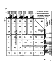
[0020} R.eferring now to Fig. 1-413 in which like elements are provided,
having like
reference designations throughout the several views, an adaptive optic (AO)
comprises a
voltage-addressable, transmissioninode, liquid-crystal (LC) cell, as is
generally known in
the art, having substrates 12 patterned into an array of indemdent pixels
generally denoted
14 to support two-dimensional (2-1 addressing for use as an .A0 actuator. In
addition to
each pixel being denoted with reference numeral 14, it should be noted that
each individual
pixel in Figs. I -413 is also provided having a unique alpha-numeric
designation, (e.g. Al ---.
3
CA 02910592 2015-10-23
WO 2014/189522 PCT/US2013/042638
[0021] In the exemplary embodiment of Figs. 1-4B, the adaptive optic is
provided
having a plurality of pixels having various shapes (squares and triangles) and
aangcd in.
columns and rows. Each of the pixels is coupled to a corresponding one of an
output of a
control circuit (not shown in Figs. 1-4B), It thould be noted that control
circuits may be
disposed on a substrate of the LC, via "flip-chip" or other chip-on-glass
assembly technique,
or else the control circuits may be "off-glass". The control circuits are
coupled to pixels 14
via electrical signal paths which. coupled control signals to conductors
disposed on the
substrate. Electrical transifions 16 and compensating resistors 20 (also
referred to as an RC
balancing resistors) fnn a portion of such signal paths to the pixels 14. Such
signal paths
may also include, for example, a flex cable coupled to a controller or other
signal source (not
visible in Fig. 1). It should be noted that e.ach. pixel 14 is individually
addressable via the
leads which are very narrow and are not clearly shown on theflgo,are.s, but
which run from
each compensating resistor to its corresponding pixel, being routed in the
narrow gaps
between pixels. Thus the. control circuit(s) are capable of providing one or
more control
signals to each of the pixels of the AO.
[0022] Each signal path couple,..d between the flex circuit and pixels
includes an RC
balancing resistor, generally denoted 20. In preferred embodiments the
resistors are
prmided having a meander-resistor layout (Fig. 413). The path lengths in the
meander-resistor layout are selected so as to result in a substantially
Lanform speml in
controlling pixels across the array. That is, the time it takes fix: any pixel
in the AO pixel
array to respond to a control signal is substantially the same regardless of
pixel location
within the A. Since these response times are equal, any effects (such as
decrease of RMS
voltage arising from delay and attenuation between the voltage SOUTCC and the
pixel) will be
equalized across all pixels, enabling compensation for such voltage decrease
in the
calibration tables already needed for any liquid-crystal device.
0023] Referring now to Figs. 3- 413, as noted above, the AO includes a
specially
designed electrode hiyout which results in uniform time constants to all
pixels across the
apeiture. As most clearly visible in Fig. 4B, a meander-resistor layout is
used to achieve
the desired uniform time constants. Each pixel has a capacitance which is
known in
advance, inVen its area and the device thickness as well as the properties of
the liquid
4
CA 02910592 2015-10-23
WO 2014/189522 PCT/US2013/042638
crystal, and thus resistors may be designed which make the product of :IliCi
the same, .where
i runs over for all pixels. Normally one would determine the resistance and
capacitance of
the pixel with the largest product (the "slowest" pixel), e.g., one of the
pixels in the center of
the aperture, whose connection to the edge. of the aperture is longest and
hence most
resistive, For this pixel, here denumerated pixel no. 1, we have some value of
RIC'. The
meander resistor chosen tbr this pixel would be of minimal resistance,
preferably zero
resistance, i.e., would be absent from the substrate layout. For each of the
other pixels,
whose intrinsic RioCi (col-noising the pixel capacitance Ci and the resistance
Rio of the
connection ftorn the edge of the aperture to the pixel without Wing a
compensating
resistor) is therefore smaller than RiC1,a compensafing resistor is included
in series with the
eonnection. Thus, all pixels are "slowed down" such that they all have
substantially the
same RC response time.
[0024] The above approach enables one to compensate for the effect of
voltage
attenuation in the RC networks in a einifor.rn rilanDer for all pixels,
enabling use of a single
calibration table for all pixels, which is a highly desirable feature for
obtaining accurate
phase control. Compensating resistors 20 may be disposed in the superstate
glue line (i.e.
a space into which sealant or "glue" is disposed to form sidewalls and couple
a superstrate to
a substrate) and resistors 20 are coupled via connecting elements 16 which
provide a
transition to leadouts (and eventually to flex circuits 18a, 1 8b and
controllers) outside of the
superstrate. As clearly vi.sible ìn Figs, 3 and 4, a total of eight meander-
resistor layout cell
types are needed for pixels in one quadrant of the AO
[0025] As noted above, an electrode layout which results in uniform time
constants to
all pixels across the aperture is used. In an optical application. in which
square beams are
used, the pixels are square to better support the intended use of the AO with.
square beams.
It should, of course, be appreciated that t3he concepts, systems and tmbniques
described
herein are not limited to square beams and that any beam. shape may be used,
Likewise, an
AO with a different pixel geometry than square may employ compensation
resistors
desigied according to this teaching. For example, a hexagonal close-packed
array, as is
known in the art, a useful geometry for an AO. The feed lines for the pixels
are of variable
length, with longer ones tl-yr the central pix.els, so the compensation
resistor technique here
taught is applicable for equalizing the response time and hence enabling more
eenvenient
CA 02910592 2015-10-23
WO 2014/189522 PCT/US2013/042638
drive voltage circuity having the same calibration table for all pixels.
[00261 Having described one or more preferred embodiments of the circuits,
techniques
and concepts described 'herein, it will now become apparent to those of
ordinary skill in the
art that other embodiments incorporating these circuits, techniques and.
concepts may be
used.. Accordingly, it is submitted that that the scope of the patent should.
not be limited to
the described embodiments, but rather, should be limited only by the spit-it
and scope of the
appended claims.
What is claimed is:
6