Note: Descriptions are shown in the official language in which they were submitted.
CA 02911731 2015-11-09
DUAL ORIENTATION CONNECTOR WITH EXTERNAL CONTACTS
[0001] This application is a divisional of Canadian Application Serial
No. 2800738,
which is the national phase of International Application PCT/US2011/038452
filed May 27,
2011 and published under International Publication No. WO 2011/150403.
BACKGROUND OF THE INVENTION
[0002] The present invention relates generally to input/output
electrical connectors such
as audio connectors and data connectors.
[0003] Standard audio connectors or plugs are available in three sizes
according to the
outside diameter of the plug: a 6.35 mm (1/4") plug, a 3.5 mm (1/8") miniature
plug and a
2.5 mm (3/32") subminiature plug. The plugs include multiple conductive
regions that
extend along the length of the connectors in distinct portions of the plug
such as the tip,
sleeve and one or more middle portions between the tip and sleeve resulting in
the
connectors often being referred to as TRS (tip, ring and sleeve) connectors.
[0004] Figs. lA and IB illustrate examples of audio plugs 10 and 20 having
three and four
conductive portions, respectfully. As shown in FIG. 1A, plug 10 includes a
conductive tip
12, a conductive sleeve 16 and a conductive ring 14 electrically isolated from
the tip 12 and
the sleeve 16 by insulating rings 17 and 18. The three conductive portions 12,
14, 16 are for
left and right audio channels and a ground connection. Plug 20, shown in FIG.
1B, includes
four conductive portions: a conductive tip 22, a conductive sleeve 26 and two
conductive
rings 24, 25 and is thus sometime referred to as a TRRS (tip, ring, ring,
sleeve) connector.
The four conductive portions are electrically isolated by insulating rings 27,
28 and 29 and
are typically used for left and right audio, microphone and ground signals. As
evident from
Figs. 1A and 1B, each of audio plugs 10 and 20 are orientation agnostic. That
is, the
conductive portions completely encircle the connector forming 360 degree
contacts such that
there is no distinct top, bottom or side to the plug portion of the
connectors.
1
CA 02911731 2015-11-09
[0005] When plugs 10 and 20 are 3.5 mm miniature connectors, the outer
diameter of
conductive sleeve 16, 26 and conductive rings 14, 24, 25 is 3.5 mm and the
insertion length
of the connector is 14 mm. For 2.5 mm subminiature connectors, the outer
diameter of the
conductive sleeve is 2.5 mm and the insertion length of the connector is 11 mm
long. Such
TRS and TRRS connectors are used in many commercially available MP3 players
and smart
phones as well as other electronic devices. Electronic devices such as MP3
players and smart
phones are continuously being designed to be thinner and smaller and/or to
include video
displays with screens that are pushed out as close to the outer edge of the
devices as possible.
The diameter and length of current 3.5 mm and even 2.5 mm audio connectors are
limiting
factors in making such devices smaller and thinner and in allowing the
displays to be larger
for a given form factor.
[0006] Many standard data connectors are also only available in sizes that are
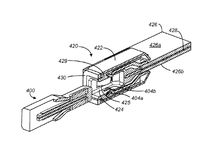
limiting
factors in making portable electronic devices smaller. Additionally, and in
contrast to the
TRS connectors discussed above, many standard data connectors require that
they be mated
with a corresponding connector in a single, specific orientation. Such
connectors can be
referred to as polarized connectors. As an example of a polarized connector,
Figs. 2A and 2B
depict a micro-USB connector 30, the smallest of the currently available USB
connectors.
Connector 30 includes a body 32 and a metallic shell 34 that extends from body
32 and can
be inserted into a corresponding receptacle connector. As shown in Figs. 2A,
2B, shell 34
has angled corners 35 formed at one of its bottom plates. Similarly, the
receptacle connector
(not shown) with which connector 30 mates has an insertion opening with
matching angled
features that prevents shell 34 from being inserted into the receptacle
connector the wrong
way. That is, it can only be inserted one way - in an orientation where the
angled portions of
shell 34 align with the matching angled portions in the receptacle connector.
It is sometimes
difficult for the user to determine when a polarized connector, such as
connector 30 is
oriented in the correct insertion position.
[0007] Connector 30 also includes an interior cavity 38 within shell 34 along
with contacts
36 formed within the cavity. Cavity 38 is prone to collecting and trapping
debris within the
cavity which may sometimes interfere with the signal connections to contacts
36. Also, and
in addition to the orientation issue, even when connector 30 is properly
aligned, the insertion
and extraction of the connector is not precise, and may have an inconsistent
feel. Further,
even when the connector is fully inserted, it may have an undesirable degree
of wobble that
may result in either a faulty connection or breakage.
2
CA 02911731 2015-11-09
[0008] Many other commonly used data connectors, including standard USB
connectors,
mini USB connectors, FireWire connectors, as well as many of the proprietary
connectors
used with common portable media electronics, suffer from some or all of these
deficiencies
or from similar deficiencies.
BRIEF SUMMARY OF THE INVENTION
[0009] Various embodiments of the invention pertain to plug connectors and
receptacle
connectors that improve upon some or all of the above described deficiencies.
Other
embodiments of the invention pertain to methods of manufacturing such plug
and/or
receptacle connectors as well as electronic devices that include such
connectors.
Embodiments of the invention are not limited to any particular type of
connector and may be
used for numerous applications. Some embodiments, however, are particularly
well suited
for use as audio connectors and some embodiments are particularly well suited
for data
connectors.
[0010] In view of the shortcomings in currently available audio and data
connectors as
described above, some embodiments of the present invention relate to improved
audio and/or
data plug connectors that have a reduced plug length and thickness, an
intuitive insertion
orientation and a smooth, consistent feel when inserted and extracted from its
corresponding
receptacle connector. Additionally, some embodiments of plug connectors
according to the
present invention have external contacts instead of internal contacts and do
not include a
cavity that is prone to collecting and trapping debris.
[0011] One particular embodiment of the invention pertains to a dual
orientation plug
connector having external contacts carried by a connector tab. The connector
tab can include
first and second opposing sides with a first set of contacts formed on the
first side and a
second set of contacts formed on the second side. The first set of contacts
can be
symmetrically spaced with the second set of contacts and the connector tab can
have a 180
degree symmetrical shape so that it can be inserted and operatively coupled to
a
corresponding receptacle connector in either of two insertion orientations. In
some
embodiments the plug connector further includes one or more ground contacts
formed on side
surfaces of the connector tab that extend between the first and second
surfaces, and in some
additional embodiments the connector tab includes a cap or ground ring that
covers the tip of
the connector and extends from the tip towards the body along at least a
portion of each of the
3
CA 02911731 2015-11-09
side surfaces. In some further embodiments, the connector tab includes at
least one retention
feature adapted to engage with a retention feature on a corresponding
receptacle connector.
[0012] In another embodiment, the invention pertains to an dual orientation
electrical
connector comprising a body and a connector tab extending longitudinally away
from the
body that includes first and second opposing surfaces. A plurality of
electrical contacts are
carried by the connector tab including a first set of external contacts formed
at the first
surface and a second set of external contacts formed at the second surface.
The connector tab
is shaped to have 180 degree symmetry and the first set of contacts is
symmetrically spaced
with the second set of contacts allowing the connector to be inserted into a
corresponding
receptacle connector in either of two orientations. In some instances, the
connector tab can
further include a side peripheral surface that extends between the first and
second opposing
surfaces and at least one ground contact formed on the side peripheral
surface. Additionally,
in some embodiments the connector still further includes a metal ground ring
that generally
defines a shape of the connector tab and includes openings on both the first
and second
surfaces in which the first and second sets of contacts are respectively
formed and surrounded
by a dielectric. Still in some other embodiments, the body includes a flexible
member or is
made from a flexible material that allows the connector to bend with respect
to an insertion
axis in which the connector is mated with a receptacle connector.
100131 In still another embodiment, the invention pertains to a dual
orientation electrical
plug connector having a body, a cable attached to the body, and an unpolarized
connector tab
extending longitudinally away from the body. The connector tab may have a
generally
rectangular cross section defined by first and second major opposing surfaces
and first and
second opposing side surfaces extending between the first and second major
surfaces. A
plurality of electrical wiping contacts can be carried by the connector tab
including a first set
of external contacts formed at the first major surface and extending parallel
to each other
along a length of the connector, and a second set of external contacts formed
at the second
major surface and extending parallel to each other along the length of the
connector. The
connector may also include first and second retention features formed on the
first and second
opposing side surfaces, respectively, that are adapted to engage with
retention features on a
corresponding receptacle connector to secure the connectors together during a
mating event.
In some embodiments, the first retention feature may also function as a first
ground contact
and the second retention feature may also function as a second ground contact.
The first set
of contacts can be symmetrically spaced with the second set of contacts, and
the fist ground
4
=
CA 02911731 2015-11-09
contact can be symmetrically spaced with the second ground contact so that the
connector tab
has 180 degree symmetry and can be inserted and operatively coupled to the
corresponding
receptacle connector in either of two positions.
[0014] Other embodiments of the invention pertain to electrical receptacle
connectors. In
one embodiment, the receptacle connector can include a housing that defines an
interior
cavity extending in a direction of the depth of the housing and a plurality of
electrical
contacts positioned within the cavity. The cavity can have a 180 degree
symmetrical shape
so that a corresponding plug connector can be inserted into the cavity in
either of two
insertion orientations. Additionally, the plurality of contacts may include a
first set of
contacts positioned at a first interior surface of the cavity and a second set
of contacts
positioned at a second interior surface of the cavity spaced apart from the
first interior surface
in an opposing relationship. The first and second sets of contacts can further
be mirror
images of each other. In some embodiments, the receptacle connector can also
include at
least one retention feature adapted to engage with a retention feature on a
corresponding plug
connector. In still other embodiments, the receptacle connector can include
first and second
retention features positioned on opposing side surfaces the cavity adapted to
engage with first
and second retention features on a corresponding plug connector.
10015] In another embodiment, the invention pertains to an electrical plug
connector that
includes a conductive cap or ground ring to isolate the connector's contacts
from interference.
The connector can further include a body and a connector tab that is attached
to and extends
longitudinally away from the body. The conductive cap can cover a tip of the
connector and
extend from the tip towards the body along at least a portion of the connector
tab's side
surfaces. A plurality of external contacts can be carried by the connector tab
at a location at
least partially surrounded by the conductive cap. In some embodiments the
plurality of
external contacts can include contacts formed at both first and second major
opposing
surfaces of the connector tab, and in some embodiments the contacts formed at
the first and
second surfaces are arranged on each surface in matching patterns.
Additionally, in some
embodiments the conductive cap can be a metal cap and in some embodiments the
connector
can further include first and second ground contacts formed on the sides of
the conductive
cap. In different embodiments the conductive cap may be a U-shaped frame or
may generally
define a shape of the connector tab except for the one or more contact regions
of the
connector tab in which the plurality of contacts are formed.
5
CA 02911731 2015-11-09
[0016] In still another embodiment, a method of manufacturing a plug
connector
having a body and a tab that is adapted to be inserted into a corresponding
receptacle
connector is disclosed. The method includes forming the connector tab to have
first and
second major opposing surfaces, third and fourth opposing side surfaces
extending
between the first and second surfaces and a 180 degree symmetrical design such
that a
plane bisecting a width of the connector tab at an angle perpendicular to the
first and
second major surfaces divides the tab into left and right portions that have
substantially
the same outer shape and a horizontal plane bisecting a height of the
connector tab at an
angle perpendicular to the third and fourth side surfaces divides the tab into
upper and
lower portions that have substantially the same outer shape; forming a first
contact
region at the first major surface of the connector tab and a second contact
region at a
second major surface of the connector tab opposite the first major surface,
the first and
second contact regions being substantially the same size and shape and
including an
equal number of contacts, wherein contacts in the first contact region are
arranged in a
first pattern according to a first spacing and contacts in the second contact
are also
arranged in the first pattern according to the first spacing; and attaching a
cable having a
plurality of insulated wires to the body so that each individual wire in the
plurality of
insulated wires is electrically connected to a contact in either the first or
second contact
regions.
[0016a] In still another aspect, the present invention provides a plug
connector
comprising: a connector tab having first and second opposing sides, and third
and fourth
opposing sides each extending between the first and second major sides,
wherein each
of the third and fourth sides are significantly narrower than either the first
or second
sides; a plurality of electrical contacts carried by the connector tab, the
plurality of
contacts including a first plurality of contacts formed on the first major
side and a
second plurality of contacts formed on the second major side, wherein the
first plurality
of contacts are symmetrically spaced with the second plurality of contacts and
the
connector tab is shaped to have 180 degree symmetry so that the connector tab
can be
inserted and operatively coupled to a corresponding receptacle connector in
either of
two orientations; and retention features formed on the third and fourth sides
near a distal
end of the connector tab that are adapted to operatively engaged with a
retention
6
CA 02911731 2015-11-09
mechanism in a corresponding receptacle connector during a mating event,
wherein the
retention features are operable as ground contacts.
[0016b] In a further aspect, the present invention provides a plug
connector
comprising: a body; a connector tab extending away from the body, the
connector tab
having width, height and length dimensions and comprising a conductive frame
having
first and second opposing sides extending in the width and length dimensions,
and third
and fourth opposing sides extending between the first and second sides in the
height and
length dimensions, the first side including a first opening and the second
side including
a second opening directly opposite the first opening; a first plurality of
external contacts
carried by the tab in a first contact region formed in the first opening of
the conductive
frame, wherein dielectric material separates each of the first plurality of
contacts from
adjacent contacts and from the conductive frame; and a second plurality of
external
contacts carried by the tab in a second contact region formed in the second
opening of
the conductive frame, wherein each contact in the second plurality of contacts
is
positioned directly opposite a contact in the first plurality of contacts and
dielectric
material separates each of the second plurality of contacts from adjacent
contacts and
from the conductive frame.
[0016c] In a still further aspect, the present invention provides a
conductive frame
for an electrical connector, the conductive frame comprising: a base portion;
and an
insertion end having 180 degree symmetry extending away from the base portion,
the
insertion end having: width, height and length dimensions; first and second
opposing
exterior surfaces extending in the width and length dimensions, the first
exterior surface
including a first opening and the second exterior surface including a second
opening
directly opposite the first opening; third and fourth opposing exterior
surfaces extending
between the first and second exterior surfaces in the height and length
dimensions; and
an end surface extending in the width and height dimensions at a distal end of
the frame
between the first and second opposing outer surfaces and between the third and
fourth
opposing outer surfaces.
[0016d] In a further aspect, the present invention provides a method of
manufacturing a plug connector having a body and a connector tab that is
adapted to be
inserted into a corresponding receptacle connector; the method comprising:
forming the
6a
CA 02911731 2015-11-09
connector tab to have first and second major opposing surfaces, third and
fourth
opposing side surfaces extending between the first and second surfaces and a
180
degree symmetrical design such that a plane bisecting a width of the connector
tab at an
angle perpendicular to the first and second major surfaces divides the tab
into left and
right portions that have substantially the same outer shape and a horizontal
plane
bisecting a height of the connector tab at an angle perpendicular to the third
and fourth
side surfaces divides the tab into upper and lower portions that have
substantially the
same outer shape; forming a first contact region at the first major surface of
the
connector tab and a second contact region at a second major surface of the
connector tab
opposite the first major surface, the first and second contact regions being
substantially
the same size and shape and including an equal number of contacts, wherein
contacts in
the first contact region are arranged in a first pattern according to a first
spacing and
contacts in the second contact are also arranged in the first pattern
according to the first
spacing; and attaching a cable having a plurality of insulated wires to the
body so that
each individual wire in the plurality of insulated wires is electrically
connected to a
contact in either the first or second contact regions.
[0016e] In a further aspect, the present invention provides a method of
plug
connector comprising: a body; a 180 degree symmetrical connector tab extending
away
from the body, the connector tab having width, height and length dimensions
and
comprising a conductive frame that defines a shape of the connector tab, the
conductive
frame having first and second opposing sides extending in the width and length
dimensions, and third and fourth opposing sides extending between the first
and second
sides in the height and length dimensions, the first side including a first
opening and the
second side including a second opening directly opposite the first opening; a
first
plurality of external contacts carried by the tab in a first contact region
formed in the
first opening of the conductive frame, the first plurality of contacts being
spaced apart
along a single row with dielectric material between each adjacent contact and
between
the contacts and the conductive frame; a second plurality of external contacts
carried by
the tab in a second contact region formed in the second opening of the
conductive
frame, the second plurality of contacts being spaced apart along a single row
with
dielectric material between each adjacent contact and between the contacts and
the
conductive frame, wherein each contact in the second plurality of contacts is
positioned
6b
CA 02911731 2015-11-09
directly opposite a contact in the first plurality of contacts; and first and
second retention
features formed in the third and fourth sides of the conductive frame and
adapted to engage
with retention features of a corresponding receptacle connector.
[0016f] In a further aspect, the present invention provides an electronic
device
comprising: a device housing; a receptacle connector having a connector
housing coupled to
the device housing, the connector housing defining an interior cavity and an
opening at a
surface of the device housing, the opening and interior cavity being shaped to
allow a
corresponding plug connector to be inserted through the opening and into the
cavity in a first
orientation and a second orientation rotated 180 degrees from the first
orientation; a plurality
of electrical contacts positioned within the interior cavity; and circuitry
operatively coupled
to the receptacle connector to, when a corresponding plug connector is mated
with the
receptacle connector, initiate a hand shaking algorithm over one of the
contacts in the
plurality of electrical contacts to determine which of the first and second
orientations the
plug connector has been mated with the receptacle connector in.
[0016g] In yet a further aspect, the present invention provides an electronic
device
comprising: a device housing; a receptacle connector having a connector
housing that
defines an interior cavity and an opening at a surface of the device housing,
the opening and
interior cavity being shaped to allow a corresponding plug connector to be
inserted through
the opening and into the cavity in a first orientation and a second
orientation rotated 180
degrees from the first orientation; a plurality of contacts positioned within
the interior cavity;
and electrical circuitry coupled to the plurality of contacts and configured
to, in response to a
mating event between the receptacle connector and the corresponding plug
connector: (i)
send a first signal over a first contact in the plurality of contacts that is
in physical contact
with a first mated contact in the corresponding plug connector and wait for a
response signal
in reply; (ii) if a response signal to the first signal is received over the
first contact, allow
signals to be transferred between the receptacle connector and the plug
connector over
additional contacts in the plurality of electrical contacts; (iii) if a
response signal to the first
signal is not received, send a second signal over a second contact in the
plurality of contacts
that is in physical contact with a second mated contact in the corresponding
plug connector
6c
CA 02911731 2015-11-09
and wait for a response in reply; and (iv) if a response signal to the second
signal is received
over the second contact, allowing signals to be transferred between the
receptacle connector
and the plug connector over additional contacts in the plurality of electrical
contacts.
[0016h] In yet a further aspect, the present invention provides an electronic
device
comprising: a device housing; a receptacle connector having a connector
housing coupled to
the device housing, the connector housing defining an interior cavity and an
opening at a
surface of the device housing, the opening and interior cavity being shaped to
allow a
corresponding plug connector to be inserted through the opening and into the
cavity in a first
orientation and a second orientation rotated 180 degrees from the first
orientation; a plurality
of contacts positioned within the interior cavity; and electrical circuitry
coupled to the
plurality of contacts and configured to: (i) send a first signal and receive a
reply to the first
signal over at least one of the plurality of contacts to determine if the plug
connector is
inserted into the interior cavity in the first orientation, and (ii) if the
connectors are mated in
the first orientation, enable the exchange of other signals between the
receptacle connector
and plug connector over other contacts in the plurality of contacts that are
coupled to
circuitry within the electronic device according to a first mapping.
[0016i] In yet a further aspect, the present invention provides a method of
determining the
insertion orientation of a plug connector that can be inserted in a receptacle
connector having
a plurality of contacts in either a first orientation or a second orientation,
the method
comprising: detecting insertion of the plug connector into the receptacle
connector; initiating
a hand shaking algorithm over a contact in the plurality of contacts to
determine which of the
first and second orientations the plug connector has been mated with the
receptacle
connector in.
[0017] To better understand the nature and advantages of the present
invention, reference
should be made to the following description and the accompanying figures. It
is to be
understood, however, that each of the figures is provided for the purpose of
illustration only
and is not intended as a definition of the limits of the scope of the present
invention. Also, as
a general rule, and unless it is evident to the contrary from the description,
where elements in
6d
CA 02911731 2015-11-09
different figures use identical reference numbers, the elements are generally
either identical
or at least similar in function or purpose.
Brief Description of the Drawings
[00181 Figs. 1 A and 1B show perspective views of previously known TRS audio
plug
connectors;
[00191 Fig. 2A shows a perspective view of a previously known micro-USB plug
connector while Fig. 2B shows a front plan view of the micro-USB connector
shown in Fig.
2A;
6e
CA 02911731 2015-11-09
[0020] Fig. 3A is simplified top view of a plug connector 40 according to one
embodiment
of the present invention;
[0021] Figs. 3B and 3C are simplified side and front views, respectively, of
connector 40
shown in Fig. 3A;
[0022] Figs. 4A-4C are front view of alternative embodiments of connector 40
according to
the present invention;
[0023] Figs. 5A-5H are simplified top views of contact layouts within contact
region 46 of
connector 40 according to different embodiments of the invention;
[0024] Fig. 6A is simplified view of contact region 46a of plug connector 50
and Fig. 6B is
simplified view of contact region 46a of plug connector 50 shown in Figs. 3A
and 3B
according to a specific embodiment of the present invention;
[0025] Figs. 7A and 7B are diagrams depicting a set of exemplary contact
locations
according to some embodiments of the present invention;
[0026] Figs. 8A-8C are simplified top, bottom and side plan views of a plug
contact
connector that includes an orientation key according to another embodiment of
the present
invention;
[0027] Figs. 9A-9F are simplified schematic representations of contact
arrangements of
connectors according to additional embodiments of the invention;
[0028] Figs. 10A and 10B are diagrams depicting a set of exemplary contact
locations
according to some other embodiments of the present invention;
[0029] Fig. 11A is a simplified side cross-sectional view of a plug connector
90 according
to one embodiment of the present invention;
[0030] Fig. 11B is a simplified side view of plug connector 90 shown in Fig.
11A that
illustrates how the connector may bend when extracted from a receptacle
connector by being
pulled in a direction that intersects the connector's axis of insertion;
[0031] Fig. 12A is simplified top view of a plug connector 100 according to
another
embodiment of the present invention;
[0032] Fig. 12B is a simplified side view of connector 100 shown in Fig. 12A;
7
CA 02911731 2015-11-09
[0033] Figs. 13A and 13B are simplified perspective views of a ground ring
that can be
included in some embodiments of the present invention;
[0034] Fig. 14A is a simplified perspective view of an audio plug connector
110 according
to one embodiment of the present invention;
[0035] Figs. 14B-14D are simplified plan views of the audio plug connector
shown in Fig.
14A;
[0036] Figs. 15A-15E are exploded perspective views of the connector 110 shown
in Fig.
14A at various stages of manufacture;
[0037] Figs. 16A-16C illustrate one example of how ground ring 102 shown in
Fig. 14A
can be formed;
[0038] Fig. 17A is a simplified perspective view of an audio plug connector
140 according
to another embodiment of the present invention;
[0039] Figs. 17B-17D, which are simplified plan views of connector 140 shown
in Fig.
17A;
[0040] Fig. 18 is a simplified cross-sectional view of connector 140 along
lines A-A'
shown in Fig. 17D;
[0041] Figs. 19A and 19B are simplified cross-sectional views of alternative
method of
connecting insulator 144 to ground ring 115 shown in Fig. 18;
[0042] Fig. 20A is a simplified perspective view of a plug connector 150
according to one
embodiment of the present invention;
[0043] Fig. 20B is an exploded view of plug connector 150 shown in Fig. 20A;
[0044] Fig. 21 is a flowchart depicting steps associated with manufacturing
connector 150
according to one embodiment of the invention;
[0045] Figs. 22A-22H are simplified perspective views of connector 150 shown
in Figs.
20A and 18B at different stages of manufacture discussed with respect to Fig.
21;
[0046] Fig. 23A is a simplified perspective view of a plug connector 190
according to
another embodiment of the invention;
[0047] Fig. 23B is an exploded view of connector plug 190 shown in Fig. 23A;
8
CA 02911731 2015-11-09
[0048] Fig. 24 is a flowchart depicting steps associated with manufacturing
connector 190
according to one embodiment of the invention;
[0049] Figs. 25A-25G are simplified perspective views of connector 190 shown
in Figs.
23A and 21B at different stages of manufacture discussed with respect to Fig.
24;
[0050] Fig. 26A is a simplified perspective view of a flexible plug connector
230 according
to another embodiment of the invention;
[0051] Fig. 26B is an exploded view of plug connector 230;
[0052] Figs. 27A-27G are simplified perspective views of connector 230 shown
in Figs.
26A and 24B at different stages of manufacture;
[0053] Fig. 28A is a simplified perspective view of a receptacle connector
jack 250
according to one embodiment of the invention;
[0054] Figs. 28B and 28C are front and bottom plan views of connector jack 250
shown in
Fig. 28A;
[0055] Fig. 29 is a simplified perspective view showing plug connector 110
inserted into
connector jack 250;
[0056] Figs. 30A-30C illustrate different positions in which the contact
overhead associated
with a receptacle connector according to the present invention may be
positioned;
[0057] Figs. 31A and 31B are front and bottom plan views of a receptacle
connector jack
200 according to one embodiment of the invention;
[0058] Fig. 32 is a simplified perspective view of a plug connector 300
according to one
embodiment of the present invention;
[0059] Figs. 33A-33C are simplified plan views of plug connector 300 shown in
Fig. 32;
[0060] Figs. 34A and 34B are diagrams depicting pin locations of connector 300
in two
different orientations according to an embodiment of the invention;
[0061] Fig. 35 is a simplified exploded perspective view of a plug connector
310 according
to another embodiment of the invention;
[0062] Figs. 36A and 36B are simplified top and side plan views of printed
circuit board
312a shown in Fig. 35 according to one embodiment of the present invention;
9
CA 02911731 2015-11-09
[0063] Fig. 37 is a flowchart depicting steps associated with manufacturing
connector 310
according to one embodiment of the invention;
[0064] Fig. 38A-38P depicts various views of plug connector 310 at different
stages of
manufacture discussed with respect to Fig. 37;
[0065] Figs. 39A-39D depict various simplified views of a receptacle connector
jack 360
according to one embodiment of the invention;
[0066] Figs. 40A-40D depict various simplified views of a receptacle connector
jack 370
according to another embodiment of the invention;
[0067] Fig. 41A-41G depicts various views of receptacle connector 360 at
different stages
of manufacture;
[0068] Fig. 42 is a simplified perspective view of a connector plug 390
according to
another embodiment of the invention.
[0069] Fig. 43 is a simplified perspective view of a connector plug 400
according to
another embodiment of the invention;
[0070] Fig. 44A is a simplified partial cut-away perspective view of plug
connector 400
and Fig. 44B is a simplified cross-sectional view of plug connector 400;
[0071] Fig. 45 is a simplified partial cut-away perspective view of plug
connector 400
inserted into a receptacle connector jack 420;
[0072] Figs. 46A-46D illustrate one example of a connector 440 having five
analog
contacts as well as a fiber optic cable 445 that runs through the center of
the connector;
[0073] Fig. 47 is a simplified perspective view of a plug connector 150
according to
another embodiment of the invention;
[0074] Fig. 48 is a simplified perspective view of a headset 160 that includes
connector 150
shown in Fig. 38 according to an embodiment of the invention;
[0075] Fig. 49A is a diagram depicting pin locations of connector 150
operating in a
Mickey bus mode according to one embodiment of the invention and Fig. 49B is a
diagram
depicting the pin locations of connector 150 operating in a legacy/backward
compatible mode
according to one embodiment of the invention;
CA 02911731 2015-11-09
[0076] Fig. 50 is a simplified perspective view of a connector plug 170
according to
another embodiment of the invention;
[0077] Fig. 51 is a simplified perspective view of a USB adapter cable 180
having a USB
connector at one end and connector 170 shown in Fig. 50 at the other end
according to an
embodiment of the invention;
[0078] Fig. 52 is a diagram depicting pin locations of connector plug 170
shown in Fig. 50
according to one embodiment of the invention;
[0079] Fig. 53 is a simplified perspective view of a connector plug 190
according to
another embodiment of the invention;
[0080] Fig. 54 is a simplified perspective view of a audio/visual adapter
cable 200 having
HDMI, USB and digital audio connectors at one end and connector 190 at the
other end
according to an embodiment of the invention;
[0081] Fig. 55 is a simplified perspective view of a audio/visual adapter
cable 210 having
mini display port and USB connectors at one end and a similar to connector 50
at the other
end according to another embodiment of the invention;
[0082] Fig. 56 is a simplified perspective view of a audio/visual adapter
cable 220 having a
mini display port connector at one end and a high speed connector at the other
end according
to another embodiment of the invention;
[0083] Fig. 57 is a diagram depicting pin locations of high speed connector
225 shown in
Fig. 56 according to one embodiment of the invention;
[0084] Fig. 58 is a simplified perspective view of a docking station 230 that
includes a plug
connector 235 according to an embodiment of the invention;
[0085] Fig. 59 is a diagram depicting pin locations of connector plug 235
shown in Fig. 52
according to one embodiment of the invention;
[0086] Fig. 60 is a simplified illustrative block diagram of an electronic
media device suitable
in which embodiments of the invention may be incorporated or used with; and
[0087] Fig. 61 depicts an illustrative rendering of one particular embodiment
of an electronic
media device suitable for use with embodiments of the present invention.
11
CA 02911731 2015-11-09
DETAILED DESCRIPTION OF THE INVENTION
[0088] The present invention will now be described in detail with reference to
certain
embodiments thereof as illustrated in the accompanying drawings. In the
following
description, numerous specific details are set forth in order to provide a
thorough
understanding of the present invention. It will be apparent, however, to one
skilled in the art,
that the present invention may be practiced without some or all of these
specific details. In
other instances, well known details have not been described in detail in order
not to
unnecessarily obscure the present invention.
[0089] In order to better appreciate and understand the present invention,
reference is first
made to Figs. 3A-3C, which are simplified top, side and front views,
respectively, of a plug
connector 40 according to one embodiment of the present invention. Connector
40 includes a
body 42 and a tab portion 44. A cable 43 is attached to body 42 and tab
portion 44 extends
away from body 42 in a direction parallel to the length of the connector 40.
Tab 44 is sized
to be inserted into a corresponding receptacle connector during a mating event
and includes a
first contact region 46a formed on a first major surface 44a and a second
contact region 46b
(not shown in Figs. 3A-3C) formed at a second major surface 44b opposite
surface 44a. A
plurality of contacts (not shown in Figs. 3A-3C) can be formed in each of
contact regions 46a
and 46b such that, when tab 44 is inserted into a corresponding receptacle
connector, contacts
in regions 46a, 46b are electrically coupled to corresponding contacts in the
receptacle
connector. In some embodiments, the plurality of contacts are self-cleaning
wiping contacts
that, after initially coming into contact with a receptacle connector contact
during a mating
event, slide further past the receptacle connector contact with a wiping
motion before
reaching a final, desired contact position.
[0090] Tab 44 also includes first and second opposing side surfaces 44c, 44d
that extend
between the first and second major surfaces 44a, 44b. While tab 44 is shown in
Figs. 3A-3C
as having a substantially rectangular and substantially flat shape, in some
embodiments of the
invention first and second major surfaces 44a, 44b may have matching convex or
concave
curvatures to them or may have a matching recessed region centrally located
between the
sides of tab 44. Contact regions 46a and 46b may be formed in the recessed
regions and the
recessed regions may, for example, extend from the distal tip of tab 44 all
the way to base 42
or may extend along only a portion of the length of tab 44 (e.g., between 'A
to 3/4 of the length
of the tab) ending at a point short of base 42. Side surfaces 44c and 44d may
also have
matching convex or concave curvatures.
12
CA 02911731 2015-11-09
[0091] Generally, the shape and curvature of surfaces 44a and 44b mirror each
other, as do
the shape and curvature of surfaces 44a and 44b, in accordance with the dual
orientation
design of connector 40 as described below. Additionally, while Figs. 3A-3C
show surfaces
44c, 44d as having a width significantly less that that of surfaces 44a, 44b
(e.g., less than or
equal to one half width of surfaces 44a, 44b), in some embodiments of the
invention side
surfaces 44c, 44d have a width that is relatively close to or even equal with
or wider than that
of surfaces 44a, 44b.
[0092] Figs. 4A-4C are simplified front plan views of embodiments of connector
40 in
which body 42 and/or tab 44 have different cross-sectional shapes. For
example, in Fig. 4A,
major surfaces 44a and 44b are slightly convex, while in Figs. 4B and 4C, side
surfaces 44c
and 44d are rounded. Further, Fig. 4C depicts an example of a connector having
recessed
regions 45a and 45b formed at major surfaces 44a and 44b, respectfully, of tab
44. The
recessed regions extend from the distal tip of tab 44 along a portion of the
length of tab 44
and are centrally located between side surfaces 44c and 44d. A person of skill
in the art will
understand that Figs. 3C and 4A-4C are but examples of suitable cross-
sectional shapes for
body 42 and tab 44 and that many other cross-sectional shapes may be employed
for each of
body 42 and tab 44 in various embodiments of the invention.
[0093] In some embodiments, one or more ground contacts can be formed on the
side
surfaces. For example, Figs. 3A and 3B show a ground contact 47a formed on
first side
surface 44c and a ground contact 47b formed on second side surface 44d
opposite ground
contact 47a. As another example, one or more ground contacts may be formed on
end
surface 44e at the distal tip of connector 40 in addition to, or instead of
ground contacts 47a,
47b. In some embodiments, each of the one or more ground contacts can be
formed on or
form part of an outer portion of its respective side surface. In other
embodiments, the one or
more ground contacts can be formed within and/or as part of a pocket,
indentation, notch or
similar recessed region formed on each of the side surfaces 44c, 44d that
operatively engage
with a retention mechanism in a corresponding receptacle connector as
described in detail
below.
[0094] Body 42 is generally the portion of connector 40 that a user will hold
onto when
inserting or removing connector 40 from a corresponding receptacle connector.
Body 42 can
be made out of a variety of materials and in some embodiments is made from a
dielectric
material, such as a thermoplastic polymer formed in an injection molding
process. While not
13
CA 02911731 2015-11-09
shown in Figs. 3A or 3B, a portion of cable 43 and a portion of tab 44 may
extend within and
be enclosed by body 42. Also, electrical contact to the contacts in each of
regions 46a, 46b
can be made to individual wires in cable 43 within body 42. In one embodiment,
cable 43
includes a plurality of individual insulated wires, one for each contact
within regions 46a and
46b, that are soldered to bonding pads on a printed circuit board (PCB) housed
within body
42. Each bonding pad on the PCB is electrically coupled to a corresponding
individual
contact within one of contact regions 46a or 46b.
[0095] Tab 44 may also be made from a variety of materials including metal,
dielectric or a
combination thereof. In some embodiments, tab 44 includes a frame made
primarily or
exclusively from a metal, such as stainless steel, and contact regions 46a and
46b are formed
within the frarne. In some other embodiments, tab 44 includes a frame made
primarily or
exclusively from a dielectric material, such as a ceramic or an elastomeric
material. For
example, tab 44 may be a ceramic base that has contacts printed directly on
its surfaces.
[0096] In embodiment illustrated in Figs. 3A and 3B, body 42 has a rectangular
cross
section that generally matches in shape but is slightly larger than the cross
section of tab 42.
As discussed with respect to Figs. 4A-4C, body 42 can be of a variety of
shapes and sizes,
however. For example, body 42 may have a rectangular cross section with
rounded or angled
edges (referred to herein as a "generally rectangular" cross section), a
circular cross section,
an oval cross section as well as many other suitable shapes. In some
embodiments, both the
body 42 and tab 44 of connector 40 have the same cross-sectional shape and
have the same
width and height (thickness). As one example, body 42 and tab 44 may combine
to form a
substantially flat, uniform connector where the body and tab seem as one. In
still other
embodiments, the cross section of body 42 has a different shape than the cross
section of tab
44. As one example, body 42 may have curved upper and lower and/or curved side
surfaces
while tab 44 is substantially flat.
[0097] Each of contact regions 46a, 46b can be centered between opposing side
surfaces
44c, 44d. Individual contacts in contact regions 46a and 46b can be external
contacts
positioned at an outer surface of tab 44 so that some embodiments of connector
40 do not
include contacts positioned within an internal cavity in which particles and
debris may
collect. Each of contact regions 46a and 46b can include one or more contacts
that can be
made from copper, nickel, brass, a metal alloy or any other appropriate
conductive material.
14
CA 02911731 2015-11-09
In some embodiments contacts can be printed on surfaces 44a and 44b using
techniques
similar to those used to print contacts on printed circuit boards.
[0098] Contact regions 46a and 46b may include any number of contacts, from
one to
twenty or more arranged in a variety of different patterns. Figs. 5A-5H
provide different
examples of contact arrangements within a contact region 46 according to
different
embodiments of the invention. As shown in Fig. 5A, contact region 46 may
include two
contacts 51(1) and 51(2) that are centered and symmetrically positioned within
the contact
region. Similarly, Fig. 5B depicts a contact region 46 having three contacts
52(1)..52(3)
centered and symmetrically positioned within the contact region, and Fig. 5C
depicts a
contact region 46 having four such contacts 53(1)..53(4).
[0099] While each of Figs. 5A-5C include a single row of contacts within
region 46, some
embodiments of the invention may include two, three or more rows of contacts.
As
examples, contact region 46 shown in Fig. 5D includes two rows of four
contacts 54(1)..54(4)
and 54(5)..54(8) with each row being centered between the sides of the contact
region and
symmetrically spaced with respect to a center line traversing the length of
the contact region;
Fig. 5E shows a contact region 46 having a first row of three contacts
55(1)..51(3) and a
second row of four contacts 55(4)..55(7) positioned within the contact region;
and Fig. 5F
depicts a contact region 46 having three rows of three contacts for a total of
nine contacts
56(1)..56(9).
[0100] While each row of individual contacts in the contact regions shown in
Figs. 5A-5F
center the contacts in the row between the sides of the contact region and
symmetrically
space the contacts with respect to a center line traversing the length of the
contact region, in
some embodiments of the invention the contacts need not be centered in this
manner. As an
example, Fig. 5G depicts a contact region 46a having two contacts 57(1)..57(2)
that are not
centered within the contact region. To provide the 180 degree symmetry
employed by some
embodiments of the invention, a connector that includes the contact region 46a
shown in Fig.
5G on one major surface, includes a contact region 46b as shown in Fig. 5H on
the opposing
major surface that matches contact region 46a. In Fig. 5H, contact region 46b
and contacts
57(3)-57(4) are shown in dashed lines to represent the position of the
contacts when looking
from contact region 46a through the connector to contact region 46b.
[0101] Each of the contact regions 46 shown in Figs. 5A-5G is representative
of both
regions 46a and 46b according to particular embodiments of the invention. That
is, according
CA 02911731 2015-11-09
to one embodiment of the invention, a plug connector 40 includes two contact
regions 46a
and 46b each of which includes two contacts as shown in region 46 in Fig. 5A.
In another
embodiment, a plug connector 40 includes contact regions 46a and 46b each of
which
includes three contacts as shown in Fig. 5B. Still other embodiments of the
invention
include: a connector 40 having contact regions 46a and 46b as shown in region
46 in Fig.
5C; a connector 40 having contact regions 46a and 46b as shown in region 46 in
Fig. 5D; a
connector 40 having contact regions 46a and 46b as shown in region 46 in Fig.
5E; a
connector 40 having contact regions 46a and 46b as shown in region 46 in Fig.
5F; and a
connector 40 having contact regions 46a and 46b as shown in region 46 in Fig.
5G.
[0102] Contacts within regions 46a, 46b may include contacts designated for a
wide variety
of signals including power contacts, ground contacts, analog contacts and
digital contacts
among others. In some embodiments, one or more ground contacts are formed in
regions 46a
and/or 46b while in other embodiments, ground contacts are only located at the
tip 44e and/or
on the side surfaces 44c, 44d of connector 40 in order to save space within
contact regions
46a and 46b for power and signal contacts. Embodiments that employ ground
contacts at one
or more positions along the peripheral side and/or tip surfaces of connector
40 instead of
within contact regions 46a and 46b may enable the overall footprint of
connector tab 44 to be
smaller than a similar connector that includes ground contacts in contact
regions 46a or 46b.
[0103] Power contacts within regions 46a, 46b may carry signals of any voltage
and, as an
example, may carry signals between 2-30 volts. In some embodiments, multiple
power
contacts are included in regions 46a, 46b to carry power signals of different
voltages levels
that can be used for different purposes. For example, one or more contacts for
delivering low
current power at 3.3 volts that can be used to power accessory devices
connected to connector
40 can be included in regions 46a, 46b as well as one or more contacts for
delivering high
current power at 5 volts for charging portable media devices coupled to
connector 40.
[0104] Examples of analog contacts that may be included in contact regions
46a, 46b
include contacts for separate left and right channels for both audio out and
audio in signals as
well as contacts for video signals, such as RGB video signals, YPbPr component
video
signals and others. Similarly, many different types of digital signals can be
carried by
contacts in regions 46a, 46b including data signals such as, USB signals
(including USB 1.0,
2.0 and/or 3.0), FireWire (also referred to as IEEE 1394) signals, SATA
signals and/or any
other type of data signal. Digital signals within contact regions 46a, 46b may
also include
16
CA 02911731 2015-11-09
signals for digital video such as DVI signals, HDMI signals and Display Port
signals, as well
as other digital signals that perform functions that enable the detection and
identification of
devices or accessories to connector 40.
[0105] In some embodiments, dielectric material is filled in between
individual contacts in
contact regions 46a, 46b so that the dielectric material and contacts form a
completely flush
outer surface of tab 44 that provides a smooth, consistent feel across the
surfaces of tab 44.
Additionally, to improve robustness and reliability, connector 40 can be fully
sealed and
includes no moving parts.
[0106] Connector 40 can have a 180 degree symmetrical, double orientation
design which
enables the connector to be inserted into a corresponding receptacle connector
in both a first
orientation where surface 44a is facing up or a second orientation where
surface 44a is
rotated 180 degrees and facing down. To allow for the orientation agnostic
feature of
connector 40, tab 44 is not polarized. That is, tab 44 does not include a
physical key that is
configured to mate with a matching key in a corresponding receptacle connector
designed to
ensure that mating between the two connectors occurs only in a single
orientation. Instead, if
tab 44 is divided into top and bottom halves along a horizontal plane that
bisects the center of
tab 44 along its width, the physical shape of the upper half of tab 44 is
substantially the same
as the physical shape of the lower half. Similarly, if tab 44 is divided into
left and right
halves along a vertical plane that bisects the center of tab along its length,
the physical shape
of the left half of tab 44 is substantially the same as the shape of the right
half. Additionally,
contacts can be positioned within contact regions 46a and 46b so that
individual contacts in
region 46a are arranged symmetric with the individual contacts in region 46b
located on the
opposite side of tab 44, and ground contacts formed at the tip or on the sides
of connector tab
44 can also be arranged in a symmetric manner.
[0107] To better understand and appreciate the 180 degree symmetrical design
of some
embodiments of the invention, reference is made to Figs. 6A and 6B which are
simplified
views of a first side 44a and an opposing second side 44b, respectively, of a
plug connector
50 according to a specific embodiment of the invention that includes four
individual contacts
formed within each of contact regions 46a and 46b. For example, as shown in
Fig. 6A,
contact region 46a may include four evenly spaced contacts 53(1)..53(4) formed
within the
region. With respect to a center plane 59 that is perpendicular to and passes
through the
middle of connector 50 along its length, contacts 53(1) and 53(2) are in a
mirrored
17
CA 02911731 2015-11-09
relationship with contacts 53(3) and 53(4). That is, the spacing from center
line 59 to contact
53(2) is the same as the spacing from center line 59 to contact 53(3). Also,
the spacing from
center line 59 to contact 53(1) is the same as the spacing from centerline 59
to contact 53(4).
Each of the pairs of contacts 53(1), 53(2) and 53(3), 53(4) are also spaced
equally from the
sides 44c and 44d of the connector with respect to each other and are spaced
equally along
the length of tab 44 between end surface 44e and body 42.
[0108] Similarly, in Fig. 6B contact region 44b includes the same number of
contacts as
region 44a that are also spaced according to the same spacing in region 44a.
Thus, contact
region 44b includes four contacts 53(5)..53(8) spaced within region 46b
according to the
same layout and spacing as contacts 53(1)..53(4) within regions 46a. Because
the layout and
spacing of contacts in regions 46a and 46b are identical, absent some sort of
indicia or mark
on one of surfaces 44a or 44b, the surfaces and contact layout on each of
surfaces 44a, 44b
looks the same. When connector 50 is inserted into a corresponding receptacle
connector, the
contacts in regions 46a, 46b will make proper electrical contact with contacts
in the
receptacle connector in either of two different orientations (referred to
herein as "up" or
"down" for convenience but it is to be appreciated that these are relative
terms intended to
connote a 180 degree change in the orientation of the connector only).
[0109] To further illustrate, reference is now made to Figs. 7A and 7B, which
schematically show a cross-sectional view of plug connector 50 having four
contacts in each
of regions 46a, 46b as depicted in Figs. 6A and 6B inserted into a matching
receptacle
connector 60. Receptacle connector 60 includes a cavity 64 into which the tab
of the plug
connector can be inserted. Four contacts 61(1)..61(4) extend from one interior
surface of the
receptacle connector into cavity 64 and four contacts 61(5)..61(8) extend from
the opposing
interior surface into cavity 64 in an oppositional and mirrored relationship
to contacts
61(1)..61(4).
[0110] Fig. 7A depicts that when the connector 50 is inserted into cavity 65
in an "up"
position, contact 53(1) of the plug connector aligns with contact 61(1) of the
receptacle
connector, contact 53(2) aligns with contact 61(2), contact 53(3) aligns with
contact 61(3)
and contact 53(4) aligns with contact 61(4). Fig. 7A also shows that, on the
opposing
surface, contact 53(5) aligns with contact 61(5), contact 53(6) aligns with
contact 61(6),
contact 53(7) aligns with contact 61(7) and contact 53(8) aligns with contact
61(8). When the
plug connector is inserted into receptacle connector 60 in a "down" position,
as shown in Fig.
18
CA 02911731 2015-11-09
7B, each contact in the plug connector still properly aligns with a contact in
the receptacle
connector. The contacts align differently, however, as follows: contact 53(5)
of the plug
connector aligns with contact 61(1) of the receptacle connector, contact 53(6)
aligns with
contact 61(2), contact 53(7) aligns with contact 61(3) and contact 53(8)
aligns with contact
61(4), while on the opposing surface, contact 53(1) aligns with contact 61(5),
contact 53(2)
aligns with contact 61(6), contact 53(3) aligns with contact 61(7) and contact
53(4) aligns
with contact 61(8). Additionally, when plug connector 50 includes side ground
contacts 53a,
53b, each side contact aligns with a corresponding side ground contact 61a,
61b from
receptacle connector 60 in either of the two possible insertion orientations
as shown in Figs.
7A and 7B.
[0111] Thus, whether connector 50 is inserted into receptacle connector 60 in
either the
"up" or "down" position, proper electrical contact is made between the
contacts in the plug
connector and the receptacle connector. Embodiments of the invention further
pertain to a
receptacle connector that includes circuitry that switches the functionality
of its pins based on
the orientation of the plug connector. In some embodiments, a sensing circuit
in the
receptacle connector or the electronic device in which the receptacle
connector is housed, can
detect the orientation of the plug connector and set software and/or hardware
switches to
switch internal connections to the contacts in the receptacle connector and
properly match the
receptacle connector's contacts to the plug connector's contacts as
appropriate. In some
embodiments the orientation of the plug connector can be detected based on a
physical
orientation key (different from a polarization key in that an orientation key
does not prevent
the plug connector from being inserted into the receptacle connector in
multiple orientations)
that, depending on the orientation of the plug connector, engages or does not
engage with a
corresponding orientation contact in the receptacle connector. Circuitry
connected to the
orientation contact can then determine which of the two possible orientations
the plug
connector was inserted into the receptacle connector.
101121 As an example, reference is now made to Figs. 8A-8C, which show
simplified top,
bottom and side plan views of a plug connector 70 according to another
embodiment of the
present inventi6n along with Figs. 9A and 9B, which are simplified schematic
views of plug
connector 70 inserted within a receptacle connector 80. Connector 70 includes
contact
regions 46a and 46b formed on opposing major surfaces of the connector that
may contain
any reasonable number of contacts. For example, in the particular embodiment
shown in Fig.
9A, connector 70 is an audio plug connector and each of contact regions 46a
and 46b include
19
CA 02911731 2015-11-09
two contacts: a microphone contact and right audio contact in region 46a, and
a left audio
contact and a ground contact in region 46b. When connector 70 is mated with
receptacle
connector 80, an orientation key 72 on the plug connector engages (or doesn't
engage) with a
corresponding orientation contact 86 within receptacle connector 80.
[0113] Circuitry operatively coupled to the receptacle connector can set
software and/or
hardware switches to properly match the receptacle connector's contacts to the
contacts of
plug connector 70. For example, a software switch can be used to switch the
connector jack's
contacts for left and right audio depending on the insertion orientation while
a hardware
switch can be used to switch the connector jacks microphone and ground
contacts to match
the contacts of connector 70. In other embodiments, both switches can be
implemented in
software or both switches can be implemented in hardware. A comparison of Fig.
9A to 9B
illustrates the switching of the receptacle contacts depending on whether or
not orientation
contact 86 is engaged (Fig. 9B) or not engaged (Fig. 9A), where for ease of
illustration, the
labels of the switched contacts are underlined and depicted in a larger font.
[0114] As another example, connector 70 can be a six contact audio plug
connector with
each of contact regions 46a, 46b including three contacts as shown in Figs. 9C-
9D: a
microphone contact, a first dedicated ground contact and a right audio contact
are within
region 46a; while a left audio contact, a second dedicated ground contact and
a second
dedicated microphone contact are located within region 46b. The first and
second ground
contacts and first and second microphone contacts align with ground and
microphone
contacts of the corresponding connector jack 80 regardless of the insertion
orientation of
connector 70. Thus, this embodiment can be carried out with a single switch,
that can be
implemented in software or hardware to switch the connector jack's contacts
for left and right
audio depending on the insertion orientation which can be detected by
orientation contact 86
within the receptacle connector.
[0115] As shown in Figs. 8A-8C, connector 70 can also include retention
features 74a, 74b
on opposing side surfaces of the connector. Retention features can operate to
secure
connector 70 in a corresponding receptacle connector as discussed below with
respect to
Figs.12A and 12B. Notably, in the embodiment shown in Figs. 8A-8C, retention
feature 74b
and orientation key 72 combine to form a single extended cutout on the side
44d of connector
70. In other embodiments, the retention feature(s) and orientation key can be
completely
separated from each other and even be included on separate surfaces. For
example, in one
CA 02911731 2015-11-09
embodiment orientation key 72 can be located on one of major surfaces 44a or
44b while the
retention features can be located on one or both of side surfaces 44c and 44d.
[0116] In other embodiments, the plug connector does not include an
orientation key and
the orientation of the connector can instead be detected by circuitry
associated with the
corresponding receptacle connector based on signals received over the
contacts. As one
example, various accessories such as headsets for cellular phones include a
microphone and
allow a user to perform basic functions such as setting earphone volume and
answering and
ending calls with the push of a button on the accessory. A single wire, serial
control chip can
be used to communicate with the host electronic device and implement this
functionality.
The chip is connected to the microphone contact (e.g., contact 112b shown in
Fig. 14A) and,
when the plug connector is inserted into the receptacle jack, can talk to
appropriate circuitry
in the jack connector or host device. Upon an insertion event, the host device
sends an
Acknowledgment signal to the serial control chip over the contact in the
receptacle connector
designated for the microphone and waits for a Response signal. If a Response
signal is
received, the contacts are aligned properly and audio and other signals can be
transferred
between the connectors. If no response is received, the host device flips the
signals to
correspond to the second possible orientation (i.e., flips the signals 180
degrees) and repeats
the Acknowledgement/Response signal routine.
[0117] In the four contact embodiment of a plug connector 70 shown in Fig. 9E,
left and
right audio contacts are always in physically reversible positions while each
of the other two
contacts is designated as a microphone contact. In this embodiment, a physical
orientation
key in the plug connector, such as key 72, can be detected by an orientation
contact or other
appropriate mechanism in the receptacle connector to determine the orientation
of the plug,
and a hardware or software switch can set the receptacle connector contacts as
appropriate for
left and right audio to correspond to the plug connector contacts. In the
embodiment of plug
connector 70 shown in Fig. 9F, a contact 75 is connected to ground through,
for example, a
ground ring 102 (described with respect to Figs. 10A-10B). When the connector
is first
plugged into a receptacle connector, circuitry associated with the receptacle
connector or the
electronic device in which the connector is housed detects the position of the
grounded
contact and switches the receptacle contacts to an appropriate orientation.
[0118] To facilitate the dual orientation feature of certain embodiments of
the invention,
contacts within contact regions 46a, 46b can be arranged such that similarly
purposed
21
CA 02911731 2015-11-09
contacts are located on opposite sides of the connector tab in a cater
cornered arrangement.
For example, referring back to Fig. 7A, contact 53(1) is in a cater cornered
arrangement with
contact 53(5) while contact 53(2) is in a cater cornered relationship with
contact 53(6).
Similarly purposed contacts are contacts that are designated to carry similar
signals.
Examples of similarly purposed contact pairs may include, first and second
power contacts,
left and right audio out contacts, first and second ground contacts, a pair of
data differential
contacts, and/or first and second digital contacts. Because of the symmetrical
relationship
between the contacts, such a cater cornered relationship ensures that for each
pair of similarly
purposed contacts in a cater cornered relationship, one of the similarly
purposed contacts will
be electrically connected to a contact in the receptacle connector that is
either dedicated to the
particular contact or can be readily switched to the particular contact. As an
example, where
contacts 53(1) and 53(5) are similarly purposed contacts that are dedicated to
left and right
audio out signals, respectively, when plug connector 50 is inserted into
receptacle connector
60, one of the audio out contacts will be in electrical contact with
receptacle contact 61(1)
and the other of the audio out contacts will be in electrical contact with
receptacle contact
61(5) regardless of whether the plug connector is mated with the receptacle
connector in an
"up" or "down" insertion orientation. Thus, both the receptacle contacts 61(1)
and 61(5) can
be audio contacts ensuring that they will be electrically coupled to an audio
contact in the
plug connector regardless of its insertion orientation.
[0119] While Figs. 7A-7B depict a particular embodiment of the invention with
an even
number of contacts in each of contact regions 46a and 46b, some embodiments of
the
invention may include an odd number of contacts in each of regions 46a, 46b.
In such
embodiments, one of the contacts on each side of the plug connector is a
central contact that
is centered around bisecting line 59a and thus aligns with a centrally located
receptacle
contact in both the "up" and "down" positions. The central contacts are not in
a cater
cornered arrangement but are in a symmetrical arrangement and can be similarly
purposed
contacts according to some embodiments of the invention.
[0120] Figs. 10A and 10B illustrate this aspect of certain embodiments of the
invention and
depict a plug connector 70 having three contacts 52(1)..52(3) and 52(4)..52(6)
formed on the
=upper and lower surfaces of tab 44 of the plug connector, respectively. When
the connector
tab is inserted into a corresponding receptacle connector 80 in an "up"
position, contacts
52(1)..52(3) align with contacts 81(1)..81(3) of the receptacle connector,
respectively, and
contacts 52(4)..52(6) align with contacts 81(4)..81(6), respectively. When the
connector tab
= 22
CA 02911731 2015-11-09
is inserted into receptacle connector 80 in a "down" position, contacts
52(4)..52(6) align with
contacts 81(1)..81(3) of the receptacle connector, respectively, and contacts
52(1)..52(3) align
with contacts 81(4)..81(6), respectively. In both orientations, plug connector
contacts 52(2)
and 52(5) align with one of the central receptacle contacts 81(2) or 81(5).
[0121] Plug connector 40 can be designed to be inserted into a matching
receptacle
connector, such as receptacle connector 80, along an insertion axis. In some
embodiments of
the invention, at least a portion of the plug connector is made from a
flexible material so that
the connector can readily bend off-axis. As an example, Fig. 11A shows a
simplified side
cross-sectional view of a connector 90 similar to connector 40 that is
intended to be inserted
into a receptacle connector along an insertion axis 95. Tab 44 of connector 90
includes a
flexible carrier member 92 that extends the length of tab 44 along with
contacts (not shown)
formed on each of the opposing surfaces 44a, 44b of connector 90 that can flex
with carrier
member 92. As an example, the contacts can be part of a flex circuit that is
bonded to
flexible carrier member 92. Flexible carrier 92 and the flexible contacts
allow tab 44 to be
bent along a direction 94 into a deformed shape as shown in Fig. 11B when the
connector is
mated with a receptacle connector 97 (i.e., positioned with an insertion
cavity 98 of the
receptacle connector) and subject to strain by being pulled in a direction 96
that intersects
insertion axis 95. As soon as the strain is relieved, tab 44 returns to its
normal shape shown
in Fig. 11A. In this manner, when connector 90 is pulled out of its receptacle
connector by
pulling at least partially sideways (e.g., along direction 96 as opposed to
pulling along axis
95) on either body 42 or the cable (not shown) attached to body 42, plug
connector 90 can
bend and pull out of the receptacle connector rather than binding within it or
eventually
breaking.
[0122] In one particular embodiment, flexible carrier 92 is a sheet of
superelastic material,
such as nitinol (an alloy of nickel and titanium present in roughly equal
amounts) and the
flexible contacts are part of a flex circuit adhered to the superelastic
sheet. Nitinol alloys
exhibit elasticity some 10-30 times that of ordinary metal which enables it to
flex under very
high strain without breaking. The flex circuit may include, for example, metal
contacts
screen printed on a thin polymide or PEEK (polyether ether ketone) layer. The
flex circuit
may be made from two separate pieces each of which is directly adhered to one
side of the
nitinol sheet or may be a single piece wrapped around the perimeter of the
nitinol sheet or
made into a sleeve that fits over the nitinol sheet.
23
CA 02911731 2015-11-09
[0123] Embodiments of the invention that include this flexibility
characteristic are not
limited to the use of any particular superelastic material and can instead use
any material that
deforms reversibly to very high strains and returns to its original shape when
the load is
removed without requiring a change of temperature to regain its original
shape. Some
embodiments of the invention may use flexible materials for carrier 92 that
are not
superelastic. For example, carrier 92 or tab 44 itself can be made from an
elastomer or
polyurethane in some embodiments.
[0124] When connector plug 90 is engaged with a corresponding receptacle
connector and
extracted at an angle to the insertion axis, more force is typically applied
to the base of the
connector than at its tip. To address this discrepancy, in some embodiments
the flexibility of
carrier 92 varies along the length of the carrier so that, for example, it is
more flexible near
the base portion or proximal end of the connector where it meets body 42 and
less flexible
near the distal end of the connector. Flexibility can be varied in this manner
by, among other
techniques, varying the materials along the length of the connector, varying
the thickness of
the flexible carrier along its length or varying the shape of the flexible
carrier along its length
or any combination of these approaches. For example, in one embodiment carrier
92 may
include a superelastic sheet near its base and a polyurethane sheet near its
distal end. The
superelastic and polyurethane sheets may overlap and be adhered together in an
area between
the proximal and distal ends. In one particular embodiment, carrier 92
comprises two sheets
of polyurethane near the distal end of tab 44 and a single sheet of nitinol
near the base of tab
44 where the tab joins body 42. At a point approximately one third of the
length of the
connector from the distal end, the nitinol sheet is sandwiched between the two
polyurethane
sheets for a portion of the length.
[0125] Reference is now made to Figs. 12A and 12B, which are simplified top
and side
views of a plug connector 100 according to another embodiment of the
invention. Plug
connector 100 includes many of the same features as plug connector 40 but
further includes a
cap 102, and first and second retention features 104a and 104b, respectively,
near a distal tip
of the connector. Cap 102 can be made from a metal or other conductive
material and can
extend from the distal tip of connector 100 along the side of the connector
towards body 42
either fully or partially surrounding contacts formed in contact regions 46a
and 46b in the X
and Y directions. Cap 102 can be grounded in order to minimize interference
that may
otherwise occur on the contacts of connector 100. In one embodiment, cap 102
may be a u-
shaped frame having a thickness that is equivalent to the thickness (T) of
connector 100. In
24
CA 02911731 2015-11-09
another embodiment, cap 102 covers the entirety of tab 44 except for contact
regions 46a,
46b and thus defines the shape of tab 44. Cap 102 is sometimes referred to
herein as a
ground ring and those two terms are intended to be used interchangeably. Cap
102 can be
formed in a variety of ways and in one embodiment can be die cast from a
metal, such as
stainless steel, that can be slid over and attached to the end of connector
tab 44 thus partially
or fully surrounding contact regions 46a and 46b at the tip and sides of the
connector.
[0126] Figs. 13A and 13B show two different embodiments of cap 102. In Fig.
13A, cap
102 is a u-shaped frame that can be attached to or slid over the end of the
connector. Cap 102
includes side portions 102a, 102b that may have varying lengths in different
embodiments.
In some embodiments sides 102a, 102b extend past contact regions 46a, 46b all
the way to
the body 42 of the connector. In other embodiments the sides may extend past
contact
regions 46a, 46b but not all the way to body 42 (as shown in Fig. 12A); may
extend exactly
to the end of contact regions 46a, 46b or may be relatively short and extend
only partially
along the length of the contact regions. Contact regions 46a, 46b lie between
the opposing
sides 102a, 102b. In still other embodiments, cap or ground ring 102 defines
the exterior
shape of tab 44 completely surrounding the contact regions 46 at the outer
surfaces of the
connector as shown in Fig. 13B.
[0127] Referring back to Figs. 12A and 12B, retention features 104a, 104b are
formed on
the opposing sides of connector 100 and are part of a retention system that
includes one or
more features on the plug connector that are adapted to engage with one or
more features on
the corresponding receptacle connector to secure the connectors together when
the plug
connector is inserted into the receptacle connector. In the illustrated
embodiment, retention
features 104a, 104b are semi-circular indentations in the side surfaces of tab
44 that extend
from surface 44a to surface 44b The retention features may be widely varied
and may
include angled indentations or notches, pockets that are formed only at the
side surfaces and
do not extend to either of the surfaces 44a, 44b upon which contact regions
46a, 46b are
formed, or other recessed regions. The retention features are adapted to
engage with a
retention mechanism on the receptacle connector that can be similarly widely
varied. The
retention mechanism(s) may be, for example, one or more springs that includes
a tip or
surface that fits within indentations 104a, 104b, one or more spring loaded
detents, or similar
latching mechanisms. The retention system, including retention features 104a,
104b and the
corresponding retention mechanism on the receptacle connector, can be designed
to provide
specific insertion and extraction forces such that the retention force
required to insert the plug
CA 02911731 2015-11-09
connector into the receptacle connector is higher than the extraction force
required to remove
the plug connector from the receptacle connector.
[01281 While retention features 104a, 104b are shown in Figs. 12A and 12B as
having a
female mating characteristic and the retention mechanism was described above
as having a
male characteristic that is moved into the retention features 104a, 104b, in
other embodiments
these roles may differ. For example, in one embodiment, retention features
104a, 104b may
be spring loaded projections that engage with a female retention mechanism on
the receptacle
connector. In still other embodiments, one of features 104a, 104b may be male-
oriented
while the other of features 104a, 104b is female-oriented. In other
embodiments, other
retention mechanisms can be used such as mechanical or magnetic latches or
orthogonal
insertion mechanisms. Additionally, while retention features 104a and 104b are
shown in
Figs. 12A and 12B as being formed in metal cap 102, in embodiments of the
invention that
do not include a metal cap or ground ring, the retention features can be
formed in whatever
structure or material makes up tab 44.
[0129] Retention features 104a, 104b can also be located at a variety of
positions along
connector 100 including along the side surfaces of tab 44 and/or top and
bottom surfaces of
tab 44. In some embodiments, retention features 104a, 104b can be located on a
front surface
42a of body 42 and adapted to engage with a retention mechanism located on a
front exterior
surface of the receptacle connector. In the embodiment illustrated in Figs.
12A and 12B,
retention features 104a, 104b are positioned within the last third of the
length of tab 44. The
inventors have determined that positioning the retention features and
corresponding latching
mechanism in the receptacle connector near the end of the plug connector helps
to better
secure the connector sideways when it is in an engaged position within the
receptacle
connector.
[0130] The description of various embodiments of the invention set forth above
with
respect to Figs. 3A-13B describes a number of different features, aspects and
variations of
different embodiments of the invention. To gain a further understanding of the
invention,
numerous additional embodiments and examples of the invention including both
audio
connector and data connector embodiments are discussed below that include some
or all of
the features already mentioned as well as additional features. The various
embodiments
discussed below include many features in common with embodiments already
discussed and
with each other. As a matter of convenience such common features are often,
but not always,
26
CA 02911731 2015-11-09
referred to with the same reference number. Additionally, in the discussion
below, reference
to a connector having a specific number of contacts generally refers to the
number of contacts
on the opposing major surfaces of the connector and does not include any
ground or other
contacts formed on the tip and/or sides of the connector.
[0131] Fig. 14A is a simplified perspective view of a four contact plug
connector 110
according to an embodiment of the invention while Figs. 14B-14D are simplified
top, side
and bottom plan views, respectively, of connector 110. As shown connector 110
includes a
tab 44 that extends from body 42. Tab 44 has a front major surface 44a upon
which two
contacts 112a and 112b are positioned and a back major surface 44b upon which
two contacts
112c and 112d are located.
[0132] The contacts can be made from a copper, nickel, brass, a metal alloy or
any other
appropriate conductive material. Spacing is consistent between each pair of
contacts 112a,
112b and 112c, 112d providing 180 degree symmetry so that plug connector 110
can be
inserted into a corresponding receptacle connector in either of two
orientations. In one
particular embodiment, connector 110 is an audio plug connector and contact
112a is a left
audio contact, contact 112b is a microphone contact, contact 112c is a right
audio contact and
contact 112d is a second, redundant microphone contact. Embodiments of the
invention are
not limited to any particular contact arrangement, however, and can be
designated for other
signals. In another four contact plug connector embodiment, connector 110 is a
data
connector and each of contacts 112a-112d can be designated for data signals.
For example,
contacts 112a and 112b can be designated for a first pair of differential data
signals (e.g., data
transmit) while contacts 112c and 112d can be designated for a second pair of
differential
data signals (e.g., data receive). In other embodiments, contacts 112a-112d
can be designated
for a wide variety of other signal types.
[0133] Metal ground ring 102 defines the shape of tab 44 and surrounds the
contacts 112a-
112d along an outer periphery of the tab. Two semi-circular notches 104a and
104b, are
formed in ground ring 102 and located on opposing sides 44c and 44d of the tab
near its distal
end. In operation, tab 44 is inserted into a receptacle connector (e.g., shown
in Figs. 28A-
28C) until notches 104a and 104b operatively engage with a retention
mechanism, such as a
cantilevered spring or detent.
[0134] In the engaged position, each of contacts 112a-112d is in electrical
contact with a
corresponding contact in the receptacle connector. Tab 44 has a 180 degree
symmetrical,
27
CA 02911731 2015-11-09
double orientation design which enables the connector to be inserted into the
connector jack
with either surface 44a or 44b on top. Additionally, the two audio contacts
112a and 112c are
located on opposite sides of the connector in a cater cornered arrangement.
Thus,
microphone contact 112d is located directly opposite audio contact 112a and
microphone
contact 112b is located directly opposite audio contact 112c. In this manner,
an audio contact
is always on the right side of the connector and a microphone contact is
always on the left
side of the connector (as oriented from the connecter base to the distal end).
A sensing circuit
in the receptacle connector or the electronic device in which the receptacle
connector is
housed, can detect the direction that the contacts 112a-112d are set and
switch internal
connections to the contacts in the connector jack appropriately as described
above.
[0135] As shown in Figs. 14A-14D, contacts 112a-112d are external contacts and
connector 110 does not include an exposed cavity in which particles and debris
may collect.
To improve robustness and reliability, connector 110 is fully sealed and
includes no moving
parts. Furthermore, connector 110 has a considerably reduced insertion depth
and insertion
width as compared to commonly available TRS and TRRS connectors. In one
particular
embodiment, tab 52 of connector 50 has a width, X, of about 2 mm; a thickness,
Y, of about
1 mm; and a insertion depth, Z, of about 4 mm. In another embodiment, tab 52
of connector
50 has a width, X, of 4.1 mm; a thickness, Y, of 1.5 mm; and a insertion
depth, Z, of 5.75
mm.
[0136] Reference is now made to Figs. 15A-15E, which show perspective views of
connector 110 at various stages of manufacture. As shown in Fig. 15A, within
connector 110
is a dielectric frame 120 that supports contacts 112a-112d. Frame 120 can be
made from any
appropriate dielectric material, such as polypropylene, and includes
respective slots (not
labeled) on the upper and lower surfaces of the frame through which each of
contacts 112a-
112d are threaded to better support the contacts. In other embodiments, frame
120 can be
made from a ceramic material and contacts 112a-112d can be printed directly
onto the frame.
[0137] Frame 120 also includes grooves 122 partially surrounding an outer
periphery at a
distal tip of the frame as well as reliefs 124a, 124b that are positioned to
align with notches
104a, 104b formed in the metal ground ring 102. Wires 126, one per contact,
extend from a
cable 43 are soldered to connection pads 128a-128d for each of the contacts
122a-112d as
shown in Fig. 15B. The metal ground ring 102, which in the embodiment shown in
Fig. 15C
is a U-shaped frame die cast from stainless steel, is then slid over the
distal end of the
28
CA 02911731 2015-11-09
connector such that slots along an interior surface of the metal ring extend
into the grooves
122 and a base portion 102b of the ground ring covers the soldered connection
pads 128a-
128d electrically coupled to contacts 112a-112d.
[0138] The connector is then overmolded (Fig. 15D) with thermoplastic polymer
130 or
similar material to provide strain relief and insulation 132, e.g., POM, is
injected around the
contacts. Finally, an ABS or similar shell 134 is positioned over and fastened
or bonded to
the base 102(b) of the tab 102 as shown in Fig. 15E using an appropriate
adhesive or other
technique to form body 42 and complete formation of the connector.
[0139] In another embodiment, the conductive ground ring 102 can be made from
a high
strength steel alloy or similar material. The ground ring can be formed in an
extrusion
process where the high strength conductive material is extruded through a
mushroom shape
mold to form a straight metal piece 135 having a mushroom shaped cross-section
as shown in
Fig. 16A. A stem section 136 of the ground ring can be designed to mate with
grooves 122
positioned along the outer periphery of dielectric frame 120 when the ground
ring is attached
to frame 120. Extruded piece 135 can then be cut to length and notched to form
u-shaped
notches 104a, 104b that align with reliefs 124a, 124b in frame 120 prior to
being bent into the
U-shape ground ring 102 as shown in Fig. 16B. Stem section 136 of the U-shaped
ground
ring 102 can then be aligned with grooves 122 of the dielectric frame so that
the ground ring
can be slid over the end of frame 120 and welded, glued or otherwise bonded to
the various
components of the connector (the particular bonding method being selected
based on the
materials being connected) as shown in Fig. 16C, which for simplicity omits
various features
of the connector such as contacts 112a-112d.
[0140] Fig. 17A is a simplified perspective view of an audio plug connector
140 according
to another embodiment of the present invention. Connector 140 is similar to
connector 110
except that it has been reinforced at the base of tab 44 to stiffen the
connector and increase its
strength in a side-load condition. Specifically, connector 140 has a thicker
base portion
102(b) underneath outer shell 134 that forms body 42. A chamfered edge 142
extends
between the thicker base portion to a connector portion of tab 44. To keep the
insertion
depth, Z, of the connector the same as that of connector 110, each of the
contacts 112a-112d
have a reduced length in connector 140 as compared to connector 110. While
none of the
figures herein are not meant to represent exact dimensions of the connectors,
the reduced
29
CA 02911731 2015-11-09
length can be seen generally by comparing Fig. 17A to Fig. 14A, which shows
connector
110.
[0141] Fig. 18, is a simplified cross-sectional view of connector 140 along
lines A-A'
shown in Fig. 17D. As evident from the cross-sectional view, ground ring 102
forms a tip
143 of the connector as well as chamfered edge 142. Insulators 144 and 145,
which can be a
single part or separate parts and can be made from a thermoplastic or similar
material,
encircle the base and tip of the tab portion of connector 140, respectively,
for cosmetic
purposes. Insulator 144 also extends within the body of connector 140,
underneath ground
ring 102 to provide the thicker base portion. In one particular embodiment,
insulators 144,
145 are made from polyoxymethylene (POM) plastic. A dielectric frame 148 runs
through
connector 140 to provide support for contacts 112a-112d. Wires 146 are
soldered to each of
the contacts 112a-112d within a cavity 149 formed at a connection pad coupled
to the
contacts that is surrounded by overmolding 147. In other embodiments, shown as
separate
examples in Figs. 19A and 19B (which show an expanded view of chamfer portion
142 of tab
44 along with a portion of outer shell 134), insulator 144 interlocks with the
ground ring to
provide a more secure connection between insulator 144 and the ground ring.
[0142] Reference is now made to Fig. 20A, which is a simplified perspective
view of a four
contact plug connector 150 according to another embodiment of the invention.
Connector
150 is generally similar to connector 110 shown in Fig. 14a except that body
42 and tab 44 of
connector 150 have features that are generally more rectangular than similar
features in
connector 110 and connector 150 includes pockets 152 formed on the sides of
tab 44 as
retention feature rather than semi-circular notches. As shown in Fig. 20A, the
edges of body
42 of connector 150 are less rounded and more rectangular than those of body
42 of
connector 110. Similarly, the edges of tab 44 in connector 150 are also less
rounded and
more rectangular than those of tab 44 in connector 110 and the tab in
connector 150 is shorter
and stubbier than that of connector 110.
[0143] Indentations or pockets 152a, 152b on each side of the connector in
ground ring 102
act as retention features, and function similarly to notches 104a, 104b in
connector 110.
Pockets 152a, 152b are adapted to operatively engage with a retention
mechanism when the
connector is mated with a corresponding receptacle connector. The retention
mechanism fits
within pockets 152a, 152b and provides a retention force that secures
connector 100 to the
matching receptacle connector. In addition to their retention feature, pockets
152a, 152b are
CA 02911731 2015-11-09
part of metal ground ring 102 and serve as ground contacts, such as contacts
47a and 47b
described with respect to Figs. 3A and 3B.
[0144] Reference is now made to Figs. 20B, which is an exploded view of
connector 150,
along with Fig. 21, which is a flow chart that illustrates steps associated
with the manufacture
of connector 150 according to one embodiment of the invention, and Figs. 22A-
22G, which
depict connector 150 at the various stages of manufacture set forth in Fig.
19. The
manufacture of connector 150 can start with the construction of a flex circuit
160 having flex
contacts 162a and 162b formed on an upper surface and a similar pair of flex
contacts (not
shown in the figures) formed on a lower surface as shown in Fig. 22A (Fig. 21,
step 170).
Flex contact 162a is electrically coupled to a solder landing 164a where a
signal wire can be
soldered to the contact by a trace (not shown) on the flex circuit. Similarly,
flex contact 162b
is electrically coupled to a solder landing 164b by a trace on flex circuit
160.
[0145] In one embodiment, flex circuit 160 is made from two substantially
identical flex
circuits 160a, 160b adhered together. For example, a first flex circuit 160a
with flex contacts
162a and 162b formed on its upper surface and no contacts formed on its
opposing surface is
adhered to a second flex circuit 160b with two flex contacts (not shown but
similar to
contacts 162a and 162b) formed on its upper surface and no contacts formed on
its opposing
surface. The two surfaces without the contacts are then joined together to
form an assembled
flex circuit 160 that has flex contacts 162a, 162b on a first surface and two
matching contacts
162c, 162d on its opposite surface.
[0146] Contact pucks 166a and 166b can then be attached to the flex circuit at
contact areas
162a, 162b, respectively, while contact pucks 166c and 166d can be attached to
contact areas
on the other side of flex circuit 160 (Fig. 21, step 172 and Fig. 22B). Pucks
166a-166d can
be made from a variety of conductive materials and in one embodiment are
nickel-plated
brass. Pucks 166a-166d can be cut to size in a stamping or similar process
from a metal sheet
and can be attached to flex circuit 160 using surface mount technology. Next,
flex circuit 160
can be inserted into ground ring 102 (Fig. 21, step 174 and Fig. 22C) and a
thermoplastic or
similar dielectric overmold 163 can formed around the contacts to provide
smooth and
substantially flat upper and lower surfaces of tab portion 44 of the connector
and provide a
finished look (Fig. 21, step 176 and Fig. 22D). In one embodiment, dielectric
overmold 163
is formed with an injection molding process using polyoxymethylene (POM).
31
CA 02911731 2015-11-09
[0147] A cable bundle 43 having four individual and insulated signal wires
161, one for
each of the contacts of connector 150, can then be attached to the ground
ring/flex circuit
assembly as shown in Fig. 22E by soldering each of the wires 161 to its
respective solder
landing, e.g., solder landings 164a-164d (Fig. 21, step 178). At this stage of
manufacture the
end of a jacket 157 of cable bundle 43 is spaced apart from flex circuit 160
in an oppositional
relationship. An inner dielectric jacket 165 is then formed around much of the
assembly
using an injection molding or similar process (Fig. 21, step 180 and Fig.
22F). Inner jacket
165 includes a generally circular end portion 167 that covers a couple
centimeters or more of
cable bundle 43 and a connector portion 169 that, combined with ground ring
102, forms a
substantially monolithic base portion 159 of connector 150. Inner jacket 165
provides
structure and strain relief for connector 150 and can be made from a
dielectric material such
as an elastomer or a polyproplylene material.
[0148] The construction of connector 150 can then be completed by sliding an
outer shell
134 around the monolithic base portion 159 covering an end base portion 102b
of ground ring
102 and inner jacket 165 (Fig. 20, step 182 and Fig.219G). Outer shell 134 can
be adhered to
the ground ring and inner jacket using any appropriate adhesive suitable for
the particular
materials being bonded.
[0149] Fig. 23A is a simplified perspective view of a plug connector 190
according to
another embodiment of the invention. Connector 190 includes many features
similar in
design and function as that of connector 150 discussed above. For example,
connector 190
includes a tab 44 having four contacts 112a-112d formed at its outer surface
and arranged on
opposing sides of the connector. Tab 44 includes a ground ring 102 that
surrounds contacts
112a-112d and includes indentations or pockets 152a, 152b of each side of the
connector tab
are adapted to operatively engage with a retention mechanism when the
connector is mated
with a corresponding receptacle connector. Connector 190 differs from
connector 150 by
including a chambered edge 192 between the tab and the body that strengthens
the connector
under side-load forces similar to chamfered edge 142 of connector 140.
[0150] Reference is now made to Figs. 23B, which is an exploded view of
connector 190,
along with Fig. 24, which is a flow chart that illustrates steps associated
with the manufacture
of connector 190 according to one embodiment of the invention and Figs. 25A-
25H, which
depict connector 190 at the various stages of manufacture set forth in Fig.
24. The
manufacture of connector 190 can start with the formation of a contact frame
194 that carries
32
CA 02911731 2015-11-09
four contact strips 196a-196d, one for each of contacts 112a-112d. Contact
frame 194 can be
made from a dielectric material and in one particular embodiment is formed
from a liquid
crystal polymer using an injection molding process. Contact strips 196a-196d
can be
stamped from a sheet of metal such as phosphor bronze and threaded into
grooves 198a-198d
formed in contact frame 194 as shown in Fig. 25A (Fig. 24, step 210).
[0151] Contact pucks 204a and 204b can be attached to one end of contact
strips 196a and
196b, respectively, while contact pucks 204c and 204d can be attached to the
corresponding
ends of contact strips 196c and 196d (Fig. 24, step 212 and Fig. 25B). Pucks
204a-204b can
be made from a variety of conductive materials and formed in a variety of
different manners.
In one particular embodiment, pucks 204a-204d are stamped from a sheet of
nickel-plated
brass and laser welded to their respective contact strips. Next, contact frame
194 can be
inserted into ground ring 102 (Fig. 24, step 214 and Fig. 25C) and a
thermoplastic or similar
dielectric overmold 200 can formed around the contacts to provide smooth and
substantially
flat upper and lower surfaces of the tab portion of the connector and provide
a finished look
(Fig. 24, step 216 and Fig. 25D). In one embodiment, dielectric overmold 200
is formed
from polyoxymethylene (POM) in an injection molding process.
[01521 Next, a cable bundle 43 having four individual insulated signal wires
161, one for
each of the contacts of connector 190, is attached to the ground ring/contact
frame assembly
as shown in Fig. 25E by soldering each of the wires 161 to its respective
contact strip (Fig.
24, step 218). An inner dielectric jacket 202 is then formed around much of
the assembly
using an injection molding or similar process (Fig. 24, step 220 and Fig.
25F). Inner jacket
202 includes a generally rounded or oval end portion 167 that covers several
centimeters or
more of cable bundle 161 and a connector portion 169 that, combined with
ground ring 102,
forms a substantially monolithic base portion 159 of connector 190. Inner
jacket 202 helps
provides strain relief for connector 190 and can be made from a dielectric
material such as an
elastomer or a polyproplylene material. The construction of connector 190 can
then be
completed by sliding an outer shell 134 around an end base portion 102b of
ground ring 102
and inner jacket 202 (Fig. 24, step 222 and Fig. 25G). Outer shell 134 can be
adhered to the
ground ring and inner jacket using any appropriate adhesive suitable for the
particular
materials being bonded.
[01531 Fig. 26A is a simplified perspective view of a four contact plug 230
according to
still another embodiment of the invention and Fig. 26B is an exploded view of
connector plug
33
CA 02911731 2015-11-09
230. Connector 150 includes many features similar to connectors 150 and 190
discussed
above with respect to Figs. 20A and 23A, respectively. Connector 123 differs
from these
connectors in that the body of connector 230 and tab portion 44 of the
connector that is
designed to be inserted within a corresponding receptacle connector are
combined as a single
monolithic (though relatively small) piece with a uniform cross-sectional
shape.
Additionally, a portion of connector 230 is relatively flexible. Specifically,
connector 230
includes a rigid connector or tip portion 232 and a flexible base portion 234.
In this particular
embodiment, rigid portion 232 is approximately one third the length of the
connector while
flexible portion 234 is approximately two thirds the length. In other
embodiments, however,
the ratio between the flexible and rigid tip portion may differ considerably.
[0154] The tip 232 of connector 230 includes a ground ring 102 that surrounds
contacts
112a-112d at the tip and sides of the connector. Ground ring 102 can be made
from any
appropriate metal or other conductive material and in one embodiment is
stainless steel plated
with copper and nickel. When fully inserted, the entirety of rigid portion 232
is within the
receptacle connector along with a portion 132 of the flexible portion 234 of
connector 230.
[0155] The flexible base portion 234 of connector 230 can be made from a
flexible dielectric
material such as an elastomer or a polyproplylene material which enables the
connector to
flex along the length of the connector to at least a point where the ground
ring begins in order
to relieve strain during off angle mating events in a manner similar to that
described with
respect to Figs. 11A and 11B. In one specific example, base portion 234 is
made from
Arnitel EL250 available from DSM Engineering. Connector 230 also includes
indentations
or pockets 152a, 152b on each side of the connector in ground ring 102 as
described above.
[0156] Reference is now made to Figs. 27A-27G, which depict connector 230 at
various
stages of manufacture. Contacts 112a-112d are formed from a flex circuit 235
upon which
contact pucks 236a-236d are attached. Pucks 236a-236d can be made from a
variety of
conductive materials and in one embodiment are brass. Pucks 236a-236d can be
cut to size in
a stamping or similar process from a metal sheet and can be attached to flex
circuit 235 using
surface mount technology (SMT) as shown in Fig. 27A. In a separate step,
ground ring 102
can be secured to the body of connector 230 by retention clips 238 which can
be made out of
the same stainless steel or other metal as the ground ring and laser welded at
locations 239 or
otherwise connected to ground ring 102 as shown in Fig. 27B. Retention clips
238 have an
34
CA 02911731 2015-11-09
anchor at one end that extends beyond the ground ring towards a base of the
connector to
secure the ground ring to the connector body as described more fully below.
[0157] Once the ground ring/retention clip and flex circuit/contact puck
assemblies are
made, the flex circuit assembly can be inserted into and adhered to the ground
ring with an
appropriate adhesive as shown in Fig. 27C. Next, a metal ground bridge 240 and
weld puck
242, each of which, for example, can be brass, are soldered together and
attached to the flex
circuit between opposing ends of retention clips 238 as shown in Fig. 17D. A
cable 43 with
signal wires 171 is then soldered to contacts 245, which are electrically
connected to and
carry signals from respective contacts 152a-152d (Fig. 27E). As shown in Fig.
27E, cable 43
has a generally flat portion that is spaced apart from flex circuit 235 in an
oppositional
relationship. An inner dielectric jacket 246 is formed around much of the
assembly using an
injection molding or similar process as shown in Fig. 27F. Inner jacket 246
extends from the
substantially flat end of cable 43 to retention clips 238 and provides
structural strength to
connector 230 covering signal wires 171 and a portion of flex circuit 235.
Inner jacket 246
can be made from a flexible dielectric material such as an elastomer or a
polyproplylene
material just like outer jacket 244, and in one particular embodiment, is made
from the same
material as the outer jacket.
[0158] The construction of connector 230 can then be completed by forming
outer jacket
244 around an end portion of cable 170, inner jacket 246 and the other
connector components
using an injection molding or similar process forming the substantially
rectangular connector
plug 230. As shown in Fig. 27G, outer jacket 244 fills in the gaps between the
contact pucks
and covers anchors 230 filling the semicircular space between each anchor end
thereby fully
securing ground ring 102 and components connected to the ground ring to the
connector
body.
[0159] Reference is now made to Fig. 28A, which is a simplified perspective
view of one
embodiment of a receptacle connector 250 that can be used in conjunction with
certain plug
connectors according to the present invention. Connector jack 250 includes a
housing 252
that defines an interior cavity 254 into which a plug connector, such as
connector 40, can be
inserted. One or more contacts extend into cavity 254 from each of the upper
and lower
interior surfaces of the cavity, the number of which depends on the type of
plug connector
receptacle connector 250 is intended to be used with. For example, receptacle
connector 250
can be designed to mate with a four contact plug connector such as connector
110 shown in
CA 02911731 2015-11-09
Figs. 14A-14D and thus includes four contacts within cavity 254 ¨ two on each
of the major
opposing interior surfaces of cavity 254 and can be designed to mate with a
four contact plug
connector such as connector 110 shown in Figs. 14A-14D. In other embodiments,
connector
jack 250 may include any number of contacts, from pairs of one to twenty or
more arranged
on opposing surfaces of cavity 254 in a variety of different patterns that
match the contact
locations of a particular plug connector. As examples, receptacle connector
250 may include
contacts at both the upper and lower interior surfaces of cavity 254 that are
positioned to
electrically couple with contacts arranged on a plug connector according to
any of the contact
patterns shown in Figs. 5A-5H as well as other contact patterns.
[0160] As seen in Fig. 28B, which is a front view of connector jack 250, in
one particular
embodiment receptacle connector 250 includes four contacts 256a-256d
positioned to
electrically couple to appropriate contacts in the corresponding plug
connector, for example
to contacts 112a-112d in connector 110. Thus, contacts 256a-256d are arranged
in a
symmetric manner complementary of contacts 112a-112d of the plug connector.
Additionally, cavity 254 is shaped so that the plug connector can be inserted
into the cavity in
either of two orientations: a first orientation in which plug connector
contacts from region
46a (contacts 112a, 112b) electrically couple to the receptacle connector
contacts protruding
from an interior upper surface of the cavity and a second orientation in which
plug connector
contacts from region 46b (contacts 112c, 112d) electrically couple to the
receptacle connector
contacts protruding from the interior upper surface. Circuitry within
receptacle connector
jack 250 detects the orientation of the plug connector and sets software
switches to properly
match the contacts to the plug connector's contacts. For example, a first
software switch can
be used to switch the connector jack's contacts for left and right audio
depending on the
insertion orientation while a second software switch can be used to switch the
connector jacks
microphone and ground contacts to match the contacts of connector 120.
[0161] To facilitate the dual orientation insertion, upper and lower portions
of cavity 254
(as defined by a plane 255 that horizontally bisects the cavity as shown in
Fig. 28B) can be
mirror images of each other. Left and right portions of cavity 254 (as defined
by a similar
plane that vertically bisects the cavity) can also be mirror images of each
other. Additionally,
receptacle connector 250 does not include polarization keys that limit a
mating event between
the plug and receptacle connectors to a single orientation.
36
CA 02911731 2015-11-09
[0162] In some embodiments receptacle connector 250 is designed to be
waterproof so as
to not allow ingress of moisture into whatever electronic device the connector
is housed
within. Also, a hole (not visible in the drawing) within the interior of
cavity 254 allows a
spring-loaded retention mechanism 258 to protrude into the cavity. As shown in
Fig. 28C,
which is a bottom plan view of receptacle connector 250, retention mechanism
258 includes a
spring 260 positioned in a cut-out section 262 of the housing. Spring 260 is
pre-loaded so
that a tip 264 extends through an opening between cut-out 262 and cavity 254.
When plug
connector 110 is inserted into cavity 254, spring 260 latches with either
retention feature
104a or 104b of the connector plug depending on its insertion orientation. In
some
embodiments, spring 260 can be made from metal and also act as a ground
contact for
receptacle connector 250.
[0163] As previously discussed, retention features 104a, 104b can be located
near the distal
end of connector 110. The inventors have determined that positioning the
retention features
near the end of the plug connector (and thus positioning the and corresponding
retention
mechanism near the rear of cavity 254) helps to better secure the plug
connector sideways
when it is in an engaged position within receptacle connector 250.
Furthermore, the shape of
the retention features on the plug connector can match the shape of retention
mechanism 258
to provide a comfortable click feel when the retention mechanism engages the
retention
feature. For example, the rounded bulbous shape of retention features 104a,
104b of
connector 110 can match the rounded shape of the tip 264 of spring 260 to
provide a secure
engagement between the structures. Fig. 29 shows plug connector 110 inserted
into
connector jack 250 where one of retention features 104a, 104b is engaged with
spring 260.
[0164] In Figs. 28A-28C, the overhead of contacts 256a-256d of receptacle
connector 250
is placed at the ends of the contacts as illustrated schematically in Fig.
30A, which shows
contacts 256a, 256b of receptacle connector 250 and their associated contact
overhead 268 in
relation to a plug connector 110 having contacts 112a, 112b operatively
coupled to the
receptacle jack. In other embodiments, the overhead of the contacts can be
placed at the sides
of the receptacle connector contacts as shown in Fig. 30B or above and below
the contacts as
shown in Fig. 30C, which is a simplified side view of plug connector 110 mated
with contacts
in a receptacle connector (where, for ease of illustration, only the contacts
of the receptacle
connector are shown in a schematic representation).
37
CA 02911731 2015-11-09
[0165] Fig. 31A is a front view of receptacle connector 270 according to
another
embodiment of the invention. Receptacle connector 270 is similar to receptacle
connector
250 except, among other differences, in the shape of cavity 254, which is
generally more
rectangular than that of connector 250, and that connector 270 includes first
and second
retention mechanisms 272a and 272b protruding into cavity 252 from opposing
side surfaces
of the cavity instead of a single retention mechanism. Each of retention
mechanisms 272a,
272b may include, for example, a spring that is pre-loaded so that a tip of
the retention
mechanism extends through an opening in each sidewall of the cavity 254. When
a plug
connector is inserted into cavity 254, the retention mechanisms 272a, 272b
latch with
retention features, such as notches 104a, 104b or pockets 152a, 152b of one of
the plug
connectors discussed above. Retention mechanisms 272a, 272b can be located
directly
opposite each other within cavity 254 and can be designed to impart a
retention force on the
plug connector that is approximately equal at each side. Similar to retention
mechanism 258,
the shape of retention mechanism 272a, 272b can match that of the plug
connector retention
features to provide a comfortable click feel when the retention mechanisms and
features
engage with each other.
[0166] Fig. 31B is a top plan view of connector jack 270. As shown in Fig.
31B, each of
the receptacle contacts 256a-256d includes a contact tip, 274a-274d,
respectively, that can be
bonded to a wire that electrically connects the contact to circuitry
associated with the
electrical device in which receptacle connector 270 is housed. For example,
connector jack
270 can be part of a portable media device and electronic circuitry associated
with the media
device is electrically connected to receptacle connector 270 via contact tips
274a-274d.
[0167] As described above, various embodiments of the invention pertain to a
connector
system having 180 degree symmetry. Thus, cavity 254 can be symmetrical with
respect to
both vertical and horizontal bisecting planes as discussed above.
Additionally, contacts 256a
and 256b can be directly opposite contacts 256c and 256d so that a plug
connector, such as
connector 230, can be inserted into jack 270 in either of two orientations. In
a first
orientation, plug connector contacts 112a, 112b are respectively coupled to
receptacle
contacts 256a, 256b and contacts 112c, 112d are respectively coupled to
receptacle contacts
256c, 256d. In a second orientation opposite the first orientation, plug
contacts 112a, 112b
are coupled to receptacle contacts 256d, 256c, while plug contacts 112c, 112d
are coupled to
receptacle contacts 256b, 256a.
38
CA 02911731 2015-11-09
[0168] While many of the embodiments of the invention set forth above have
been depicted
in the included figures as four contact connectors, embodiments of the
invention are not
limited to any particular number of contacts. To further underscore this,
reference is now
made to Figs. 33A-33D, which depict various views of a twelve contact plug
connector 300
according to one embodiment of the present invention. Specifically, Fig. 33A
is a simplified
perspective view of plug connector 300 while Figs. 33B-33D are simplified
bottom, front and
side plan views, respectively. Connector 300 includes many of the same
features as
connector 150 except it has six contacts 302(1) and 302(6) positioned within
contact region 46a
and an additional six contacts 302(7) and 302(12) positioned within region 46b
on the opposing
surface of tab 44. The contacts can be made from a copper, nickel, brass, a
metal alloy or any
other appropriate conductive material. Spacing is consistent between each of
the contacts on
the front and back sides and between the contacts and the edges of the
connector providing
180 degree symmetry so that plug connector 300 can be inserted into a
corresponding
receptacle connector in either of two orientations as discussed above.
[0169] A significant portion of tab 44 is including its shape is defined by
ground ring 102
that extends from a distal tip of the connector towards the outer shell and
partially surrounds
contacts 302(0..302(12) along an outer periphery of tab 44. Ground ring 102
can be made from
any appropriate metal or other conductive material and in one embodiment is
stainless steel
plated with copper and nickel. Two indentations or pockets 152a and 152b are
formed in
ground ring 102 and located on opposing sides 56c and 56d of the tab near its
distal end as
with connector 150. In one particular embodiment, tab 44 of connector 300 has
a width, X,
of 4.0 mm; a thickness, Y, of 1.5 mm; and a insertion depth, Z, of 5.0 mm. It
is understood
that the dimensions of connector 50 as well as the number of contacts may vary
in different
embodiments.
[0170] When connector 300 is properly engaged with a receptacle connector each
of
contacts 302(1)-302(12) is in electrical contact with a corresponding contact
in the
corresponding receptacle connector. Tab 52 has a 180 degree symmetrical,
double
orientation design which enables the connector to be inserted into a connector
jack in both a
first orientation where surface 44a is facing up or a second orientation where
surface 44b is
facing up. In the first orientation, plug connector contacts 302(1)- 302(6)
couple to receptacle
contacts 366(1)-366(6), respectively, and contacts 302 (7)- 302 (12) couple to
receptacle contacts
366(7)-366(12), respectively. In the second orientation opposite the first
orientation, plug
39
CA 02911731 2015-11-09
contacts 302(1)- 302(6) couple to receptacle contacts 366(7)-366(12) and plug
contacts 302(7)-
302(12) couple to receptacle contacts 366(1)-366(6).
[0171] To facilitate the orientation agnostic feature of connector 300,
contacts 302(1)-
302(12) are arranged such that similarly purposed contacts are located on
opposite sides of the
connector in a cater cornered arrangement. As an example, reference is made to
Fig. 34A,
which is a diagram depicting pin locations of connector 300 according to one
specific
embodiment of the invention having two contacts designated for power, two
contacts
designated for analog audio signals and eight contacts designated for
differential data signals
including two USB data contacts, and six display port contacts.
[01721 As shown in Fig. 34A, when a midpoint line 305 dividing connector tab
44 into
equal top and bottom halves and a midpoint line 306 dividing the connector tab
44 into equal
left and right halves are considered, the contacts associated with connector
50 can be divided
into four quadrants labeled clockwise from the top left portion of the
connector as quadrants
I, II, III and IV, respectively. Quadrants I and III are located in a cater
cornered arrangement
as are quadrants II and IV. Individual contacts within the cater cornered
quadrants can be
arranged, based on their function, in a mirrored relationship. For example,
the two contacts
in quadrants I and III closest to midpoint line 61, contacts 302(3) and
302(9), are each
dedicated for power. Similarly the two outermost contacts in these quadrants
are dedicated
for a pair of differential data signals. In quadrants, II and IV, the
innermost contact, contacts
302(4) and 302(10) are each dedicated for analog audio signals while the two
outermost
contacts in each quadrant dedicated for a pair of differential data signals.
[0173] As evident from a comparison of Figs. 34A and 34B, which depict the
pinout of
connector 300 in two different orientations (in Fig. 34A surface 44a is facing
up while in Fig.
34B surface 44b is facing up), regardless of which of the two possible
orientations that
connector 300 is inserted into its receptacle connector, the contact order on
the top side of the
connector, from left to right, is always as follows: the first two contacts
are designated for a
pair of differential data signals, the third contact is designated for a power
contact, the fourth
contact is designated for an audio contact and the fifth and sixth contacts
are designated for
another pair of differential data signals. Similarly, the contact order on the
bottom side of the
connector, from left to right, is always as follows: the first two contacts
are designated for a
pair of differential data signals, the third contact is designated for an
audio contact, the fourth
CA 02911731 2015-11-09
contact is designated for a power contact and the fifth and sixth contacts are
designated for
another pair of differential data signals.
[0174] Reference is now made to Figs. 35-38. Fig. 35 is an exploded view of
connector
310 for a synchronization and charging cable that has the same form factor as
connector 300
(and thus will operatively engage with the same set of receptacle connectors
as plug
connector 300) including the same number of contacts. As a sync and charge
cable, however,
the contact locations dedicated for audio contacts and display port contacts
are not needed
and thus are not made operational in this particular embodiment. Fig. 37 is a
flow chart that
illustrates steps associated with the manufacture of connector 310 according
to one
embodiment of the invention and Fig. 38A-38P depicts connector 310 at the
various stages of
manufacture set forth in Fig. 37.
[0175] The manufacture of connector 310 can start with the construction of
printed circuit
boards 312a and 312b (Fig. 37, step 330) each of which includes six contact
areas that,
together, correspond to contacts 302(1)- 302(12). Figs. 36A and 36B more
clearly show a top
plan view and side plan view, respectively, of PCB.312a. Contact pucks are
attached to the
contact areas of PCB 312a to form contacts 302(1)-302(6). The contact pucks
can be made
from a variety of conductive materials and in one embodiment are nickel-plated
brass. The
pucks can be cut to size in a stamping or similar process from a metal sheet
and can be
attached to PCB 312a using surface mount technology. As shown in Fig. 36A, PCB
312a
includes wire solder pads 315 that are electrically coupled to corresponding
contact areas. As
noted above because connector 310 is a sync and charge cable, connector 310
does not
include electrical connections for audio contacts 302(4) and 302(10), nor does
it include
electrical connections for display port contacts 302(1)-302(2), 302(7)-302(8)
and 302(11)-302(12).
Instead, contacts formed in those locations are not coupled to solder pads on
the PCBs and
are thus not functional. This is evidenced in Fig. 36A which shows USB
contacts 302(5)-
302(6) and power contact 302(3) coupled to corresponding solder pads via
electrical traces
while contacts 302(1), 302(2) and 302(4) are not connected to electrical
traces and are not
connected to any of solder pads 315. In other embodiments, all of contacts
302(1)-302(12) may
be operatively coupled to solder pads on the PCBs or different subsets of
contacts may be
coupled depending on the purpose of the connector.
[0176] After each of the PCBs 312a, 312b are constructed and the contacts
attached, the
PCBs are inserted through the front side of ground ring 102 via the top and
bottom openings
41
CA 02911731 2015-11-09
of the ground ring that surround the contacts as shown in Fig. 38A-38F. Next,
ground plate
314 is sandwiched between the two PCBs 312a, 312b by inserting the ground
plate from the
back of ground ring 102 (Fig. 38G). Ground plate 314 provides a thick layer of
shielding
between contacts 302(1)-302(6) formed on PCB 312a and contacts 302(7)-302(12)
formed on
PCB 312b.
[0177] The assembled ground ring/PCB/ground plate structure (Fig. 38H) is then
placed in
a molding tool and a thermoplastic or similar dielectric overmold 316 can be
formed around
the contacts to provide smooth and substantially flat upper and lower surfaces
of the tab
portion of connector 310 and provide a finished look (Fig. 37, step 334; Fig.
381). In one
embodiment, dielectric overmold 316 is formed with an injection molding
process using
polyoxymethylene (POM).
[0178] A cable bundle 318 having individual signal wires 320, one for each of
the
functional contacts of connector 310 as well as one or more ground wires to be
coupled to
ground ring 102 can be prepared at this time or prior to step 330 (Fig. 38J).
The individual
signal wires are cut and stripped, the jacket of the cable bundle is stripped
and the cable
shields are folded back over the jacket. Next, a cable crimp 322 having a
bottom metal shield
is secured to the cable bundle (Fig. 37, step 336; Fig. 38K). The cable bundle
can then be
attached to the ground ring/PCB assembly as shown in Fig. 38L by soldering
each of the
signal wires to its respective solder pad and soldering the ground wires to
the ground ring
(Fig. 37, step 338). The solder joints and exposed wires can then be potted
with a UV glue to
further secure the connections.
[0179] At this stage of manufacture the end of cable bundle 318 is spaced
apart from the
PCB assembly in an oppositional relationship and positioned above bottom metal
shield 312
and between two opposing ends of ground ring 102. A metal top shield 314 can
be attached
to the top of ground ring 102 (Fig. 38M) and the top and bottom metal shields
are laser
welded or similarly attached to ground ring 102 to form an enclosure or box
around the cable
bundle (Fig. 37, step 340). Next, a dielectric trim piece 326 can be slid over
the end of tab
102 and glued to the exposed front of ground ring 102 (Fig. 37, step 342; Fig.
38N). As
shown in Fig. 38N, dielectric trim includes two rails 326a, 326b that slide
into corresponding
grooves in ground ring 102 and includes a front face 326c that is sized to
have the same width
and height as the base of ground ring 102. In one embodiment trim piece 326
can be made
from ABS plastic or a similar dielectric material.
42
CA 02911731 2015-11-09
[0180] An inner dielectric strain relief jacket 328 is then formed around much
of the
assembly using an injection molding or similar process (Fig. 37, step 344;
Fig. 380). Strain
relief jacket 328 can include a generally circular end portion 328a that
covers a centimeter or
more of cable bundle 318 and a block portion 328b that completes and fills in
gaps in the
metal enclosure formed by ground ring 102, bottom shied 322 and top shield 324
thereby
forming a substantially monolithic base portion 90 of connector 310 that is
effectively sealed.
Strain relief jacket 328 provides structure and strain relief for connector
310 and can be made
from a dielectric material such as an elastomer or a polyproplylene material.
[0181] The construction of connector 310 can then be completed by sliding an
outer shell
134 around the monolithic base portion covering an end portion of ground ring
102, trim
piece 326 and strain relief jacket 328 (Fig. 37, step 346; Fig. 38P). Outer
shell 134 can be
formed from ABS or a similar dielectric material and adhered to the ground
ring and inner
jacket using any appropriate adhesive suitable for the particular materials
being bonded.
[0182] Figs. 39A-39D show top, perspective, front and side views of a
receptacle connector
360 according to one embodiment of the invention designed to have a reduced
width as
compared to depth. Receptacle connector 360 includes a housing 362 that
defines a cavity
364 and houses twelve contacts 366(1)-366(12) within the cavity. In operation,
a connector
plug, such as plug connector 300 can be inserted into cavity 364 to
electrically couple the
contacts 302(1)-302(12) to respective contacts 366(1)-366(12). Positioned
along the sides of the
interior of cavity 364 are two spring-loaded conductive retention clips 368a,
368b that
protrude into the cavity and function to both secure the plug connector within
the cavity and
provide a ground for the connector.
[0183] Retention mechanisms 368a, 368b may include, for example, a metal
spring that is
pre-loaded so that a tip of the retention mechanisms extend through an opening
in each
sidewall of the cavity 364. When a plug connector is inserted into cavity 364,
the retention
clips 368a, 368b latch with pockets 152a, 152b, respectively, of the connector
plug. The
shape of retention mechanism 368a, 368b matches that of pockets 152a, 152b to
provide a
comfortable click feel when the retention clips engage with the pockets. In
one embodiment,
the depth and position of the pockets is selected to provide specific
insertion and extraction
forces such that the retention force required to insert the plug connector
into receptacle
connector 360 is higher than the extraction force required to remove the plug
connector from
the receptacle connector. Also, in one embodiment, retention clips 368a, 368b
are located
43
CA 02911731 2015-11-09
near the back surface of cavity 364. The inventors have determined that
positioning the
retention clips near the back of the cavity, which requires pockets 152a, 152b
on the plug
connector to be positioned near its distal end, helps to better secure the
connector sideways
when it is in an engaged position within connector jack 360.
[0184] Each of the receptacle contacts 366(1)-366(12) electrically connects
its respective plug
contact to circuitry associated with the electrical device in which receptacle
connector 360 is
housed. For example, receptacle connector 360 can be part of a portable media
device and
electronic circuitry associated with the media device is electrically
connected to jack 360 by
soldering tips of contacts 366(1)-366(12) that extend outside housing 362 to a
multilayer board
such as a printed circuit board (PCB) within the portable media device.
Additionally, each of
the conductive retention clips 368a, 368b can be electrically coupled to a
ground path
associated with connector 360. As an example, in one embodiment, pins at a
back end of
retention clips 368a, 368b can be soldered to bonding pads formed on the
multilayer board or
PCB associated with the portable media device that are coupled to ground.
[0185] Figs. 40A-40D show top, perspective, front and side views of a
receptacle connector
370 according to another embodiment of the invention designed to have a
reduced depth as
compared to width. Except for the dimensions of housing 363, the components of
connector
370 are similar to those of connector 360 and are thus referred to with the
same reference
numbers.
[0186] In one embodiment, each of receptacle connectors 360 and 370 can be
formed using
the process depicted in Fig. 41. For example, contacts 366(1)-366(12) can be
formed from lead
frames stamped from an appropriate metal such as nickel-coated brass (Fig.
41A). The
contacts can be arranged and spaced apart in a mold and insert molded within
dielectric
blocks 369 made from a thermoplastic or similar material to form two separate
sets of
contacts (Fig. 41B). Each of the contact sets can then be attached at top and
bottom interior
surfaces of housing 362 (Fig. 41C) so that a front end of the contact extends
into cavity 364
formed by the housing and a back end of the contact extends out of the back of
the housing so
that it can be soldered to a bonding pad (not shown) formed on a printed
circuit board or
similarly electrically connected to desired circuitry associated with the
electronic device in
which the receptacle connector is housed.
[0187] Retention clips 368a, 368b can similarly be formed using a metal
stamping process
and assembled to the sides of housing 362 (Fig. 41D). Retention clips 368a,
368b can
44
CA 02911731 2015-11-09
include pins 367 that extend out past a back end of housing 362 in order to
electrically
ground the retention clips to the electrical device in which receptacle
connector 360 is housed
as discussed above. Next, the partially assembled receptacle connector can be
placed in a
mold and liquid silicone rubber can be injected around the housing to form a
boot 380 that
seals the receptacle connector (Fig. 41E). Top and bottom metal shells 382 and
384 can then
be attached over silicone rubber boot 380 to the top and bottom of housing
362, respectively,
and laser welded together to form an outer enclosure that provides additional
shielding for the
connector (Fig. 41F). Finally, a conductive EMI gasket 386 can be attached to
the front of
the housing to further seal the connector when receptacle connector and the
plug connector
are mated (Fig. 41G).
[0188] Fig. 42 is a simplified perspective view of a connector plug 390
according to
another embodiment of the invention in which a ground ring is not employed.
Instead,
connector 390 is made from two printed circuit boards 392a, 392b sandwiched
around a
structural conductive member 264, such as a brass plate. A tab portion 395
extends out of
body 42 and has the same form factor as tab 44 of connector 300 shown in Fig.
32 including
the same twelve contacts (six on an upper surface of connector 390 and six on
a lower
surface) spaced the same distance from the edges of the connector at the same
spacing
enabling plug connector 390 to be operatively coupled to the same receptacle
connectors such
as plug connector 300.
[0189] Connector 390 does not include a ground ring similar to ground ring
102, however.
Instead, indentations 396a, 396b formed on opposing sides of conductive member
394 match
generally the size and contour of pockets 152a, 152b giving the tab portion of
connector 390
a bread loaf shape when viewed from above or below. Indentations 266 provide
the
connector the same comfortable click/lock feeling achieved by connector 300
when it is
inserted and removed from a receptacle connector. Also, when mated with a
receptacle
connector, conductive member 394 receives a ground connection via the
retention clips in the
receptacle connector.
[0190] Another example of a data connector according to the present invention
is illustrated
in Fig. 43, which is a perspective view of a connector 400 according to
another embodiment
of the invention. Connector 400 includes eight contacts arranged as four pairs
of contacts
401, 402 on a first major surface of tab 44 and 403 and 404 (not shown in Fig.
43) on the
CA 02911731 2015-11-09
opposing major surface. In one embodiment, each of the contact pairs carry
complementary
or similarly purposed signals. For example, in one particular embodiment
contact pair 401
includes first and second power signals, contact pair 402 includes a first set
of positive and
negative differential data signals, signal pair 403 includes a second set of
positive and
negative differential data signals, and contact pair 404 includes a third set
of positive and
negative differential data signals (contact pairs 403 and 404 are not shown in
Fig. 43 but are
directly opposite contact pairs 401 and 402). The data contacts can be used to
carry any
appropriate data signal as well as audio signals, video signals and the like.
From an exterior
view, other than the number of contacts, connector 400 is similar to connector
300 and
includes a ground ring 102, an outer sleeve 216 and pockets 217 that are
similar to the
components of the same name in connector 300. Additionally, ground ring 102
includes a
chamfered edge 192 to increase the strength of the connector.
[0191] Fig. 44A is a simplified perspective cut-away view of connector 400 in
which
individual contacts 402a and 402b from contact pair 402 are fully visible
without surrounding
molding or the ground ring. Each of the contacts is attached to a printed
circuit board 405
having a ground plane 408 sandwiched between top and bottom dielectric layers
406a and
406b. Contacts 401a, 401b and 402a, 402b are attached to conductive pads (not
shown)
formed on dielectric layer 406a while contact 403a, 403b and 404a, 404b are
attached to
conductive pads formed on dielectric layer 406b. Ground plane 408 is thus
positioned
between the sets of contacts pairs (401 and 404) and (402 and 403) which
reduces signal
interference that may otherwise occur between the closely spaced contact
pairs.
[0192] Fig. 44B is a simplified cross-sectional view of connector 400 through
the middle of
the contact pairs. As shown in Fig. 44B, contact pairs 401-404 are divided
into four
quadrants by ground plane 404 and a central rib 415a, which is part of ground
ring 102. Rib
415a runs longitudinally through the tab portion of connector 400 dividing the
tab into left
and right halves with contact pairs 401 and 404 on one half and contact pairs
402 and 403 on
the opposite half. Fig. 44B also shows that dielectric overmolding 418 (e.g.,
a thermoplastic
material such as POM) fills in gaps between the individual contacts of each
contact pair (e.g.,
between contacts 401a and 401b) as well as between the contact pairs and
ground ring 102
and rib 415a.
[0193] Reference is now made to Fig. 45, which is a simplified partial cut-
away perspective
view of a plug connector 400 and a receptacle connector jack 420 according to
an
46
CA 02911731 2015-11-09
embodiment of the invention where plug connector 400 is positioned next to
connector jack
420 prior to a mating event. Connector jack 420 includes an outer shell 422
that defines an
interior cavity 424 into which the tab portion of plug connector 400 can be
inserted. The
receptacle connector includes four contact pairs 426-429 that extend into
cavity 424 and
detents 425 which extend from the opposing sidewalls of jack 420 into cavity
424. When
plug connector 400 is inserted into cavity 424, detents 425 engage pockets
152a, 152b to
secure the plug connector within cavity 424 and individual contacts in contact
pairs 401-404
of the plug connector are electrically coupled to individual contacts of
contact pairs 426-429,
respectively, of the receptacle connector.
[0194] Each of the contacts in contact pairs 426-429 can be is insert molded
within a
dielectric block 429 made from a thermoplastic or similar material with a
front end of the
contact extending into cavity 424 and a back end extending in the opposite
direction towards
a back end of the receptacle connector. In Fig. 45 only individual contacts
402b and 404a,
404b of receptacle connector 420 can be seen. The back end of each contact is
electrically
coupled to a bonding pad (not shown) formed on printed circuit board (PCB)
426.
Conductive traces (not shown) on PCB 426 connect the contacts to circuitry
associated with
the electronic device in which receptacle connector 420 is housed. To reduce
signal
interference between contacts and improve grounding, receptacle connector 430
includes
grounding contacts and a ground plane 428 that generally surround the contact
pairs and
divide them into quadrants that correspond to the quadrants associated with
contacts 401-404.
Specifically, a grounding contact can be located between each contact pair and
a sidewall of
housing 422 while other grounding contacts can be located between contact
pairs 403, 404
and 401, 402, respectively. Each of the grounding contacts is positioned to
contact a different
portion of ground ring 102 when the connectors are mated. Grounding plane 428
is formed
on PCB 426 and sandwiched between an upper dielectric layer 426a and a lower
dielectric
layer 426b. Finally, a conductive gasket 430 provides sealing and
environmental shielding
when jack 420 and plug connector 400 are mated.
[0195] Any of the connectors discussed herein can be modified to include one
or more fiber
optic cables that extend through the connector and can be operatively coupled
to receive or
transmit optical data signals between a mating connector jack. As an example,
Figs.
46A-46D illustrate one example of a connector 440 having five analog contacts
as well as a
fiber optic cable 445 that runs through the center of the connector. The
analog contacts
include contacts 112a, 112c for left and right audio, a contact 112b for
microphone, a contact
47
CA 02911731 2015-11-09
112d for power, and a contact 222e for ground. Fiber optic cable 230 allows
for high data
rate transmissions and can be used for USB 4.0 compatibility (e.g.,
10GB/second data
transfer). With power, audio and data connections, connector 440 can be used
to charge a
device while simultaneously providing data and audio functions.
[0196] As shown in Fig. 46D, which is an expanded view of the distal end of
connector
440, fiber optic cable 445 terminates at a lens 446 positioned at the distal
end of the
connector and secured in place by ground ring 425. Lens 446 can be made from a
chemically
strengthened aluminosilicate glass or a similar material that is highly
resistant to scratching
and is flush with the external surface of ground ring 425 to prevent debris
build-up and
abstraction of light.
[0197] Some embodiments of the invention pertain to connectors specifically
designed for
specific functions, for example as required by certain accessories or cable
adapters, as
described below with respect to Figs. 47-59. In the described embodiments and
unless
otherwise noted, each of the connectors described with respect to Figs. 47-59
includes a
connector tab that is similarly designed in shape and dimensions to tab 44 of
plug connector
300 shown in Fig. 32, including contact spacing and side retention pockets, so
that the
various connector tabs are generally insertable and useable with the same
receptacle
connector as plug connector 300. Also, each of the connectors described in
Figs. 47-59
includes a ground ring that enables the connector to be connected to ground
via grounded
retention clips in a corresponding receptacle connector as described above.
[0198] As a first example of a specifically purposed connector, Fig. 47 is a
simplified
perspective view of a plug connector 500 according to an embodiment of the
invention
specifically designed for headphones and other audio applications. Connector
500 includes
four contacts, two contacts on an upper surface of a tab portion 502 of the
connector and two
contacts on the lower surface of connector tab 502. The four contacts provide
left and right
audio as well as microphone power, and are sized and spaced such that they
match the
locations of contacts 302(3) and 302(4) on one side and match the location,
size and spacing of
contacts 302(9) and 302(10) on the other side. Thus, as shown in Fig. 49A, the
two contacts on
each side can be used to represent power and audio and align (depending on the
orientation of
connector 500) with either the power and audio contacts shown in Fig. 34A or
shown in Fig.
34B. In one embodiment, circuitry associated with an electronic device in
which connector
500 can be plugged into allows the contacts to be used in a backward
compatible mode where
48
CA 02911731 2015-11-09
the power contact is replaced with a Microphone Bias contact as shown in Fig.
49B. Fig. 48
is a simplified perspective view of a headset 510 that includes connector 500
shown in Fig.
47 according to an embodiment of the invention including left and right
earbuds 512, 514
connected to connector 500 by a cable 516.
[0199] Fig. 50 is a simplified perspective view of a connector plug 520
according to
another embodiment of the invention that is specifically adapted to be used in
data
synchronization applications and charging applications. To this end, connector
520 includes
fully functional contacts at the two locations designated for USB data that
align with contact
locations 302(5) and 302(6) and the two locations designated for power that
align with
contact locations 302(3) and 302(9) as shown in Fig. 52 as well as ground
contacts that
connect to connector 520 through its ground ring via the receptacle connector
retention clips
as described above. As configured, connector 520 allows for USB 2.0
synchronization as
well as 5 volt, 2 amp charging. Fig. 51 is a simplified perspective view of a
USB adapter
cable 530 having a USB male connector 535 at one end and connector 520 shown
in Fig. 50
at the other end according to an embodiment of the invention. The two
connectors are
connected together by a cable 532.
[0200] Fig. 53 is a simplified perspective view of a connector plug 540 that
supports full
audio/video functionality according to another embodiment of the invention
including line
out audio, Mikey bus control and a two channel display port as well as USB 2.0
synchronization, 5 volt, 2 amp charging and a 3 volt accessory out signal.
Connector 540
includes active circuitry (not shown) within a shell 542 that allows for
conversion of display
port video signals to HDMI signals. Connector 540 includes the full complement
of twelve
functional contacts as shown in Figs. 34A and 34B. Fig. 54 is a simplified
perspective view
of a audio/visual adapter cable 600 having an HDMI connector 602, a USB
connector 604
and a digital audio connector 606 at one end connected by a cable 608 to
connector 540 at the
other end according to an embodiment of the invention. Active circuitry within
shell 542 of
connector 540 separates audio and digital data send over the six display port
data contacts of
connector 540 sending the audio signals to both the digital audio connector
606 and HDMI
connector 602 while sending the video signals to HDMI connector 602. The USB
data
signals can be passed through the USB contact pins of connector 540 directly
to USB
connector 604.
49
CA 02911731 2015-11-09
[0201] Fig. 55 is a simplified perspective view of a audio/visual adapter
cable 610 having a
mini display port connector 612 and a USB connector 614 at one end connected
by a cable
618 to a plug connector 616 having a pinout as shown in Figs. 34A and 34B at
the other end
according to another embodiment of the invention. Fig.56 is a simplified
perspective view of
a audio/visual adapter cable 620 having a mini display port connector 622 at
one end
connected by a cable 628 to a high speed data connector 626 at the other end
according to
another embodiment of the invention. Connector 626 has a pinout that includes
two high
speed differential data input contacts and two high speed differential data
output contacts as
shown in Fig. 57 instead of display port contacts. The high speed data
contacts allow for data
transfer rates of up to 10GB/second thereby allowing 5 GB/sec data transfer
using the PCI-
express 2.0 standard and 8 GB/sec data transfer using the PCI-express 3.0
standard. Active
circuitry embedded in the shell of connector 626 converts the PCI-express
signals as
necessary to other data formats such as minidisplay port signals.
[0202] Fig. 58 is a simplified perspective view of a docking station 630 that
includes a
connector tab 635 according to an embodiment of the invention that has the
same form factor
and contact arrangement as tab 44 in Fig. 32. Tab 635 extends upward from a
surface 632
upon which a portable electronic device may be placed when docked in station
630 with tab
635 mated with a receptacle connector incorporated into the portable media
device. A second
surface 634 can support a back of the electronic device while docked.
[0203] Docking station 630 allows a portable media device, such as an iPod or
MP3 player
or an iPhone or other smart phone to be connected to a host computer via
connector 635.
Connector 635 supports the full complement of twelve contacts set forth in
Figs. 34A and
34B and thus allows for line out audio, Mikey bus control and a two channel
display port as
well as USB 2.0 synchronization, 5 volt, 2 amp charging and a 3 volt accessory
out signal. In
another embodiment, docking station 630 does not provide full audio/video
support and
instead provides charging and USB data transfer as well as audio out and
legacy/UART
(universal asynchronous receiver/transmitter) control. Fig. 59 is a diagram
depicting pin
locations of connector tab 635 shown in Fig. 58 according to this additional
embodiment with
reduced contact pins in tab 635.
[0204] While the discussion of various particular connectors for accessories,
cable adapters
or other devices set forth above with respect to Figs. 47-59 specifically
included twelve
contact connectors having a connector layout compatible with that of plug
connector 300
CA 02911731 2015-11-09
discussed with respect to Figs. 32-34B, embodiments of the invention are not
so limited. In
other embodiments, similar or identical accessories, cable adapters and other
devices may
include connectors having twelve contacts arranged in a different layout than
connector 300
or having contacts dedicated to different signals or signals arranged in a
different order.
Additionally, still other embodiments include similar or identical
accessories, cable adapters
and other devices that include connectors with fewer or more contacts than
connector 300. A
person of skill in the art will readily recognize these and other alternative
embodiments of the
present invention based on the disclosure herein.
[0205] Embodiments of the invention are suitable for a multiplicity of
electronic devices,
including any device that receives or transmits audio, video or data signals
among others. In
some instances, embodiments of the invention are particularly well suited for
portable
electronic media devices because of their potentially small form factor. As
used herein, an
electronic media device includes any device with at least one electronic
component that may
be used to present human-perceivable media. Such devices may include, for
example,
portable music players (e.g., MP3 devices and Apple's iPod devices), portable
video players
(e.g., portable DVD players), cellular telephones (e.g., smart telephones such
as Apple's
iPhone devices), video cameras, digital still cameras, projection systems
(e.g., holographic
projection systems), gaming systems, PDAs, desktop computers, as well as
tablet (e.g.,
Apple's iPad devices), laptop or other mobile computers. Some of these devices
may be
configured to provide audio, video or other data or sensory output.
[0206] Fig. 60 is a simplified illustrative block diagram representing an
electronic media
device 700 that includes an audio plug receptacle 705 according to embodiments
of the
present. Electronic media device 700 may also include, among other components,
connector
receptacle 710, one or more user input components 720, one or more output
components 725,
control circuitry 730, graphics circuitry 735, a bus 740, a memory 745, a
storage device 750,
communications circuitry 755 and POM (position, orientation or movement
sensor) sensors
760. Control circuitry 730 may communicate with the other components of
electronic media
device 700 (e.g., via bus 740) to control the operation of electronic media
device 700. In
some embodiments, control circuitry 730 may execute instructions stored in a
memory 745.
Control circuitry 730 may also be operative to control the performance of
electronic media
device 700. Control circuitry 730 may include, for example, a processor, a
microcontroller
and a bus (e.g., for sending instructions to the other components of
electronic media device
51
CA 02911731 2015-11-09
700). In some embodiments, control circuitry 730 may also drive the display
and process
inputs received from input component 720.
[0207] Memory 745 may include one or more different types of memory that may
be used
to perform device functions. For example, memory 745 may include cache, flash
memory,
ROM, RAM and hybrid types of memory. Memory 745 may also store firmware for
the
device and its applications (e.g., operating system, user interface functions
and processor
functions). Storage device 750 may include one or more suitable storage
mediums or
mechanisms, such as a magnetic hard drive, flash drive, tape drive, optical
drive, permanent
memory (such as ROM), semi-permanent memory (such as RAM) or cache. Storage
device
750 may be used for storing media (e.g., audio and video files), text,
pictures, graphics,
advertising or any suitable user-specific or global information that may be
used by electronic
media device 700. Storage device 750 may also store programs or applications
that may run
on control circuitry 730, may maintain files formatted to be read and edited
by one or more of
the applications and may store any additional files that may aid the operation
of one or more
applications (e.g., files with metadata). It should be understood that any of
the information
stored on storage device 750 may instead be stored in memory 745.
[0208] Electronic media device 700 may also include input component 720 and
output
component 725 for providing a user with the ability to interact with
electronic media device
700. For example, input component 720 and output component 725 may provide an
interface
for a user to interact with an application running on control circuitry 730.
Input component
720 may take a variety of forms, such as a keyboard/keypad, trackpad, mouse,
click wheel,
button, stylus or touch screen. Input component 720 may also include one or
more devices
for user authentication (e.g., smart card reader, fingerprint reader or iris
scanner) as well as an
audio input device (e.g., a microphone) or a video input device (e.g., a
camera or a web cam)
for recording video or still frames. Output component 725 may include any
suitable display,
such as a liquid crystal display (LCD) or a touch screen display, a projection
device, a
speaker or any other suitable system for presenting information or media to a
user. Output
component 725 may be controlled by graphics circuitry 735. Graphics circuitry
735 may
include a video card, such as a video card with 2D, 3D or vector graphics
capabilities. In
some embodiments, output component 725 may also include an audio component
that is
remotely coupled to electronic media device 700. For example, output component
725 may
include a headset, headphones or ear buds that may be coupled to electronic
media device
700 with a wire or wirelessly (e.g., Bluetooth headphones or a Bluetooth
headset).
52
CA 02911731 2015-11-09
[0209] Electronic media device 700 may have one or more applications (e.g.,
software
applications) stored on storage device 750 or in memory 745. Control circuitry
730 may be
configured to execute instructions of the applications from memory 745. For
example,
control circuitry 730 may be configured to execute a media player application
that causes
full-motion video or audio to be presented or displayed on output component
725. Other
applications resident on electronic media device 700 may include, for example,
a telephony
application, a GPS navigator application, a web browser application and a
calendar or
organizer application. Electronic media device 700 may also execute any
suitable operating
system, such as a Mac OS, Apple i0S, Linux or Windows and can include a set of
applications stored on storage device 750 or memory 745 that is compatible
with the
particular operating system.
[0210] In some embodiments, electronic media device 700 may also include
communications circuitry 755 to connect to one or more communications
networks.
Communications circuitry 755 may be any suitable communications circuitry
operative to
connect to a communications network and to transmit communications (e.g.,
voice or data)
from electronic media device 700 to other devices within the communications
network.
Communications circuitry 755 may be operative to interface with the
communications
network using any suitable communications protocol such as, for example, Wi-Fi
(e.g., a
802.11 protocol), Bluetooth, high frequency systems (e.g., 900 MHz, 2.4 GHz
and 5.6 GHz
communication systems), infrared, GSM, GSM plus EDGE, CDMA, quadband and other
cellular protocols, VOIP or any other suitable protocol.
[0211] In some embodiments, communications circuitry 755 may be operative to
create a
communications network using any suitable communications protocol.
Communications
circuitry 755 may create a short-range communications network using a short-
range
communications protocol to connect to other devices. For example,
communications
circuitry 755 may be operative to create a local communications network using
the Bluetooth
protocol to couple with a Bluetooth headset (or any other Bluetooth device).
Communications circuitry 755 may also include a wired or wireless network
interface card
(NIC) configured to connect to the Internet or any other public or private
network. For
example, electronic media device 700 may be configured to connect to the
Internet via a
wireless network, such as a packet radio network, an RF network, a cellular
network or any
other suitable type of network. Communication circuitry 745 may be used to
initiate and
53
CA 02911731 2015-11-09
conduct communications with other communications devices or media devices
within a
communications network.
[0212] Electronic media device 700 may also include any other component
suitable for
performing a communications operation. For example, electronic media device
700 may
include a power supply, an antenna, ports or interfaces for coupling to a host
device, a
secondary input mechanism (e.g., an ON/OFF switch) or any other suitable
component.
[0213] Electronic media device 700 may also include POM sensors 760. POM
sensors 760
may be used to determine the approximate geographical or physical location of
electronic
media device 700. As described in more detail below, the location of
electronic media device
700 may be derived from any suitable trilateration or triangulation technique,
in which case
POM sensors 760 may include an RF triangulation detector or sensor or any
other location
circuitry configured to determine the location of electronic media device 700.
[0214] POM sensors 760 may also include one or more sensors or circuitry for
detecting
the position orientation or movement of electronic media device 700. Such
sensors and
circuitry may include, for example, single-axis or multi-axis accelerometers,
angular rate or
inertial sensors (e.g., optical gyroscopes, vibrating gyroscopes, gas rate
gyroscopes or ring
gyroscopes), magnetometers (e.g., scalar or vector magnetometers), ambient
light sensors,
proximity sensors, motion sensor (e.g., a passive infrared (PIR) sensor,
active ultrasonic
sensor or active microwave sensor) and linear velocity sensors. For example,
control
circuitry 730 may be configured to read data from one or more of POM sensors
760 in order
to determine the location orientation or velocity of electronic media device
700. One or more
of POM sensors 760 may be positioned near output component 725 (e.g., above,
below or on
either side of the display screen of electronic media device 700).
[0215] Fig. 61 depicts an illustrative rendering of one particular electronic
media device
780. Device 780 includes a multipurpose button 782 as an input component, a
touch screen
display 784 as a both an input and output component, and a speaker 785 as an
output
component, all of which are housed within a device housing 790. Device 780
also includes a
primary receptacle connector 786 and an audio plug receptacle 788 within
device housing
790. Each of the receptacle connectors 786 and 788 can be positioned within
housing 790
such that the cavity of the receptacle connectors into which a corresponding
plug connector is
inserted is located at an exterior surface of the device housing. In some
embodiments, the
cavity opens to an exterior side surface of device 780. For simplicity,
various intemal
54
CA 02911731 2015-11-09
components, such as the control circuitry, graphics circuitry, bus, memory,
storage device
and other components are not shown in Fig. 61. Receptacle connectors according
to
embodiments of the invention are particularly suitable to be used as either or
both of primary
receptacle 786 or audio plug receptacle 788. Additionally, in some
embodiments, electronic
media device 780 has only a single receptacle connector that is used to
physically interface
and connect the device (as opposed to a wireless connection) to the other
electronic devices.
Embodiments of the invention are also particularly suitable for such a
connector.
102161 As will be understood by those skilled in the art, the present
invention may be
embodied in many other specific forms without departing from the essential
characteristics
thereof. As an example, while a number of embodiments illustrated above
included ground
contacts that were incorporated into the retention features, both in the plug
connector as well
as the receptacle connector, other embodiments of the invention may include
ground contacts
along portions of the side or tip of the connector that is not part of a
retention mechanism.
Similarly, some embodiments may not include any contacts at all on the side of
the connector
tab and instead may include both signal and ground contacts on the first and
second major
opposing surfaces of the connector tab. In such embodiments, ground contacts
can be located
within the contact regions 46a, 46b and/or may be located at one or more
locations on major
sides 44a, 44b outside of contact regions 46a, 46b.
[0217] Also, while a number of specific embodiments were disclosed with
specific
features, a person of skill in the are will recognize instances where the
features of one
embodiment can be combined with the features of another embodiment. For
example, some
specific embodiments of the invention set forth above were illustrated with
pockets as
retention features. A person of skill in the art will readily appreciate that
any of the other
retention features described herein, as well as others not specifically
mentioned, may be used
instead of or in addition to the pockets. Also, those skilled in the art will
recognize, or be
able to ascertain using no more than routine experimentation, many equivalents
to the
specific embodiments of the inventions described herein. Such equivalents are
intended to be
encompassed by the following claims.