Note: Descriptions are shown in the official language in which they were submitted.
CA 02911829 2015-11-12
275537
SYSTEM AND METHOD FOR UNIFIED COMMON
MODE VOLTAGE INJECTION
BACKGROUND
[0001] Embodiments of the disclosure relate generally to systems and
methods of
unified common mode voltage injection to achieve multiple functions.
[0002] Power converters, particularly multi-level power converters, are
increasingly
used for performing power conversion in a wide range of applications due to
the
advantages of high power quality waveform and high voltage capability. For
example,
multi-level power converters may be used for performing DC-to-AC power
conversion to
supply single-phase or multi-phase AC voltages to electric motors in vehicles
and/or
pumps. Multi-level converters may also be used in power generation systems
such as
wind turbine generators and solar generators for performing DC-to-AC power
conversion
to supply single-phase or multi-phase AC voltages for power grid transmission
and
distribution.
[0003] Typically, the power converters are designed to regulate or control
various
characteristic parameters in association with the operation of the power
converters to
meet certain requirements and/or ensure reliable operations. For example, a
neutral point
current between at least two DC capacitors on a DC link is controlled to
minimize a
voltage difference between the two DC capacitors to avoid stressing of the
switching
devices and/or creation of undesired harmonic signals. The neutral point
current
balancing is achieved by multiple control strategies, one of which includes
injecting a
common mode voltage in the multi-level converter to balance the neutral point
current.
However, different control strategies are applied to determine the common mode
voltage
for different level converters. For example, a control strategy for a three
level converter
is different from a control strategy for a seven level converter which results
in
undesirable costs and computations. In one approach, a unified common mode
voltage
injection technique may be applied to control the neutral point current in n-
level
1
CA 02911829 2015-11-12
275537
converters. Different local optimum limits corresponding to different level
converters
may be used during computation of the common mode voltage to balance the
neutral
point current. And the calculation methods of neutral point current are
different for
different level converters as well because of different switching functions
and different
switching states. Such an approach leads to complex computations as
computation
methods for balancing the neutral point current are different for different
level converters
as each converter includes different switching functions and switching states.
[0004] Hence, there is a need for an improved system and control
methodology to
address the aforementioned issues.
BRIEF DESCRIPTION
[0005] In accordance with one aspect of the present disclosure, a power
conversion
system is provided. The power conversion system includes at least one multi-
level power
converter and a controller coupled to the at least one multi-level power
converter. The
controller includes a first common mode voltage (CMV) injection module and a
second
CMV injection module. The first CMV injection module is for generating a first
CMV
signal for modifying at least one voltage command to achieve a first function
in
association with operation of the power conversion system. The second CMV
injection
module is for generating a second CMV signal based at least in part on a three-
level
CMV limit either for modifying the at least one voltage command or for further
modifying the at least one modified voltage command to achieve a second
function in
association with operation of the power conversion system.
[0006] In accordance with another aspect of the present disclosure, a
method for
operating a power conversion system having a multi-level converter and a
controller
coupled thereto is provided. The method includes: generating a first common
mode
voltage (CMV) injection signal; using the first CMV signal to modify at least
one voltage
command to achieve a first function in association with operation of the power
conversion system; generating a second CMV signal based at least in part on a
three-level
2
CA 02911829 2015-11-12
275537
CMV limit; and using the second CMV signal either to modify the at least one
voltage
command or to further modify the at least one modified voltage command to
achieve a
second control function in association with operation of the power conversion
system.
[0007] In accordance with another aspect of the present disclosure, another
power
conversion system is provided. The power conversion system includes a direct
current
(DC) link, at least one multi-level power converter, and a controller. The DC
link
includes at least a first DC part and a second DC part defining a neutral
point
therebetween. The at least one multi-level power converter is coupled to the
DC link.
The controller is coupled to the at least one multi-level power converter and
includes a
common mode voltage (CMV) injection module configured for generating a CMV
signal
for modifying at least one voltage command to balance DC voltages at the first
DC part
and the second DC part. The CMV injection module provides at least one of a
maximum
and minimum CMV limit signal for limiting the magnitude of the CMV signal
based at
least in part on a three-level CMV limit.
DRAWINGS
[0008] These and other features, aspects, and advantages of the present
disclosure
will become better understood when the following detailed description is read
with
reference to the accompanying drawings in which like characters represent like
parts
throughout the drawings, wherein:
[0009] FIG. 1 is a block diagram of a power conversion system configured to
implement a unified common mode voltage injection algorithm/method in
accordance
with an exemplary embodiment of the present disclosure;
[0010] FIG. 2 is a detailed circuit diagram of a converter having a nested
neutral
point piloted configuration that may be used in the power conversion system
shown in
FIG. 1 in accordance with an exemplary embodiment of the present disclosure;
3
CA 02911829 2015-11-12
275537
[0011] FIG. 3 is a detailed circuit diagram of a converter having another
nested
neutral point piloted configuration that may be used in the power conversion
system
shown in FIG. 1 in accordance with another exemplary embodiment of the present
disclosure;
[0012] FIG. 4 illustrates a detailed circuit diagram of a seven-level
nested NPP phase
leg that may be used in the three-phase power converter in accordance with one
embodiment of the present disclosure;
[0013] FIG. 5 is a detailed circuit diagram of a seven-level phase leg of a
three-phase
converter having another nested neutral point piloted configuration that may
be used in
the power conversion system shown in FIG. 1 in accordance with another
exemplary
embodiment of the present disclosure;
[0014] FIG. 6 is a detailed circuit diagram of a converter having another
nested
neutral point piloted configuration that may be used in the power conversion
system
shown in FIG. 1 in accordance with another exemplary embodiment of the present
disclosure;
[0015] FIG. 7 is a detailed circuit diagram of a converter having another
nested
neutral point piloted configuration that may be used in the power conversion
system
shown in FIG. 1 in accordance with another exemplary embodiment of the present
disclosure;
[0016] FIG. 8 is a block diagram of an unified common mode voltage
injection
module in accordance with another exemplary embodiment of the present
disclosure;
[0017] FIG. 9 is a block diagram illustrating detailed structures of a
second CMV
injection module shown in FIG. 8 in accordance with one exemplary embodiment
of the
present disclosure;
4
CA 02911829 2015-11-12
275537
[0018] FIG. 10 is an exemplary graphical representation depicting a three
level CMV
limit as applied to a three-level converter in accordance with another
exemplary
embodiment of the present disclosure;
[0019] FIG. 11 is an exemplary graphical representation depicting a three
level CMV
limit as applied to a five-level converter in accordance with an exemplary
embodiment of
the present disclosure;
[0020] FIG. 12 is an exemplary graphical representation depicting a three
level CMV
limit as applied to a seven-level converter in accordance with an exemplary
embodiment
of the present disclosure; and
[0021] FIG. 13 is a flowchart illustrating a unified common mode voltage
injection
method in accordance with one exemplary embodiment of the present disclosure.
DETAILED DESCRIPTION
[0022] Embodiments disclosed herein generally relate to a unified common
mode
voltage (CMV) injection method and a power conversion system that can be
configured
to implement the unified CMV injection method to achieve multiple purposes or
functions in association with the operation of the power conversion system.
More
specifically, the unified CMV injection method may be implemented to inject a
first
CMV signal which is used to modify at least one command signal or modulation
signal
such as three-phase voltage commands to achieve a first function in
association with the
operation of the power conversion system. In one embodiment, the first
function may be
increasing the DC voltage utilization or reducing the total harmonic
distortion (THD)
which may be achieved by injecting the first CMV signal generated through a
min-max
calculation. In the min-max calculation, the first CMV signal is generated
according to
an instantaneous maximum voltage and an instantaneous minimum voltage
identified
from a plurality of voltage signals such as three-phase voltage signals. In
other
embodiments, the first CMV signal may be generated by injecting a pure third-
order
harmonic signal which has a three times fundamental frequency. In some
embodiments,
CA 02911829 2015-11-12
275537
to achieve minimum output THD, the first CMV signal may be injected in a
particular
manner to ensure the modified command signal or the modified modulation signal
does
not reach the edges of the carrier band. In some embodiments, to further
reduce the
switching loss in operating the switching devices of the power converter, the
first CMV
signal may be generated in a particular manner to provide a flattop
modulation. Flattop
modulation refers to maintaining the gate signals of at least one phase
unchanged either at
the "0" state or "1" state for a sufficiently long time.
[0023] In addition, the unified CMV injection method may be implemented to
inject a
second CMV signal. This second CMV signal is used to either modify the at
least one
command or modulation signal prior to the modification by the first CMV signal
or to
further modify the already modified CMV signal by the first CMV signal to
achieve at
least a second function in association with the operation of the power
conversion system.
In some embodiments, the second function may be neutral point current
regulation or DC
link voltage balancing. More specifically, in one embodiment, the second CMV
signal
may be injected to regulate a DC current flowing to or from the neutral point
at the DC
link to make the voltage difference at the DC link substantially zero over one
or more
control cycles. In another embodiment, the second CMV signal may be injected
to
regulate an AC current flowing to or from the neutral point at the DC link to
make the
voltage difference at the DC link substantially zero over one or more control
cycles. In
some embodiments, the second CMV signal may be injected in a particular manner
to
ensure the gate signals generated through PWM modulation have a minimal pulse
width
without creating voltage-second distortion at the output of the power
converter. In some
embodiments, the second CMV signal is injected to have a minimal magnitude to
avoid
the creation of undesired THD, but create the same effect of neutral point
current
regulation or DC voltage balancing.
[0024] In some embodiments, during generation of the second CMV signal, a
three-
level CMV local optimum limit is taken into consideration. The magnitude of
the second
CMV signal is particularly generated so that one or more modified modulation
voltage
6
CA 02911829 2015-11-12
275537
signals will not exceed a voltage range defined by a maximum modulation
voltage limit
and minimum modulation voltage limit. Further, the magnitude of the second CMV
signal is particularly generated to ensure either the maximum
modulation/voltage signal
or a minimum modulation/voltage signal modified by the second CMV signal does
not
cross zero.
[0025] Implementing the unified CMV injection method can achieve a variety
of
technical advantages and/or benefits. One technical advantage or benefit is
the DC
voltages of the DC link can be balanced at any power factor. Another technical
advantage or benefit is the CM voltage seen from the load can be minimized
since an
average neutral point current instead of an instantaneous neutral point
current is
compensated, and the capacitor charging/discharging current is not taken in
consideration
for neutral point current compensation. Yet another technical advantage or
benefit in
association with injecting CMV signals by considering the three-level CMV
limit is
avoiding additional switching patterns and/or transients, and reducing control
complexity.
Other technical advantages or benefits will become apparent to those skilled
in the art by
referring to the detailed descriptions and accompanying drawings provided
below in
accordance with one or more embodiments of the present disclosure.
[0026] In an effort to provide a concise description of these embodiments,
not all
features of an actual implementation are described in the one or more specific
embodiments. It should be appreciated that in the development of any such
actual
implementation, as in any engineering or design project, numerous
implementation-
specific decisions must be made to achieve the developers' specific goals,
such as
compliance with system-related and business-related constraints, which may
vary from
one implementation to another. Moreover, it should be appreciated that such a
development effort might be complex and time consuming, but would nevertheless
be a
routine undertaking of design, fabrication, and manufacture for those of
ordinary skill
having the benefit of this disclosure.
7
CA 02911829 2015-11-12
275537
[0027] Unless defined otherwise, technical and scientific terms used herein
have the
same meaning as is commonly understood by one of ordinary skill in the art to
which this
disclosure belongs. The terms "first," "second," and the like, as used herein
do not
denote any order, quantity, or importance, but rather are used to distinguish
one element
from another. Also, the terms "a" and "an" do not denote a limitation of
quantity, but
rather denote the presence of at least one of the referenced items. The term
"or" is meant
to be inclusive and mean either any, several, or all of the listed items. The
use of
"including," "comprising" or "having" and variations thereof herein are meant
to
encompass the items listed thereafter and equivalents thereof as well as
additional items.
The terms "connected" and "coupled" are not restricted to physical or
mechanical
connections or couplings, and can include electrical connections or couplings,
whether
direct or indirect. Furthermore, the terms "circuit" and "circuitry" and
"controller" may
include either a single component or a plurality of components, which are
either active
and/or passive and may be optionally be connected or otherwise coupled
together to
provide the described function.
[0028] FIG. 1 illustrates a block diagram of a power conversion system 100
in
accordance with an exemplary embodiment of the present disclosure. The power
conversion system 100 may be any appropriate converter-based system that can
be
configured to implement the unified common mode voltage injection method as
disclosed
herein. In some embodiments, the power conversion system 100 may be a multi-
level
converter-based system suitable for high power and high voltage applications.
The multi-
level power converter may be a three/five/seven-level or N-level neutral point
clamped
(NPC) converter, a three/five/seven-level or N-level neutral point pilot (NPP)
converter, a
three/five/seven-level or N-level active neutral point clamped (ANPC)
converter, a
three/five/seven-level or N-level cascaded H-bridge (Chain-link) converter, or
any other
type of multi-level converter in which a DC link is composed of one positive
rail, one
negative rail and one neutral point.
8
CA 02911829 2015-11-12
275537
[0029] As illustrated in FIG. 1, the power conversion system 100 includes a
power
conversion device 120 and a control device 140 coupled in communication with
the
power conversion device 120. In one embodiment, the control device 140 is
arranged to
be in communication with the power conversion device 120 and may transmit
control
signals 106 to the power conversion device 120 via one or more electrical
links or wires
for example. In another embodiment, the control device 140 may be in optical
communication with the power conversion device 120 and can transmit the
control
signals 106 to the power conversion device 120 via an optical communication
link, such
as one or more optical fibers for example. In another embodiment, the control
device 140
may be embedded within the power conversion device 120. The control device 140
may
include any suitable programmable circuits or devices such as a digital signal
processor
(DSP), a field programmable gate array (FPGA), a programmable logic controller
(PLC),
and an application specific integrated circuit (ASIC). The power conversion
device 120
can be operated to perform unidirectional or bidirectional power conversion
between a
first power device 110 and a second power device 130 in response to the
control signals
106 transmitted from the control device 140.
[0030] In one embodiment, as shown in FIG. 1, the power conversion device
120
may include a first converter 122, a DC link 124, and a second converter 126.
In one
embodiment, the first converter 122 may be an AC-DC converter (also known as
rectifier) which is configured to convert first electric power 102 (e.g.,
first AC electric
power) provided from the first power device 110 (e.g., power grid) into DC
electric
power 123 (e.g., DC voltage). In one embodiment, the DC-link 124 may include
one or
more capacitors coupled in series and/or in parallel. The DC-link 124 is
configured to
remove ripples from first DC voltage 123 and supply second DC voltage 125 to
the
second converter 126. In one embodiment, the second converter 126 may be a DC-
AC
converter (also known as inverter) which is configured to convert the second
DC voltage
125 into a second AC voltage 104, and supply the second AC voltage 104 to the
second
power device 130 (e.g., AC electric motor) or to a power network such as a
load and/or
utility grid (not shown). Although not illustrated in FIG. 1, in some
embodiments, the
9
CA 02911829 2015-11-12
275537
power conversion system 100 may include one or more other devices and
components.
For example, one or more filters and/or circuit breakers can be placed between
the first
power device 110 and the power conversion device 120. Also, one or more
filters and/or
circuit breakers can be placed between the power conversion device 120 and the
second
power device 130.
[0031] The power conversion system 100 illustrated in FIG. 1 can be used in
a variety
of applications, for example, in a motor drive for driving motors such as AC
motors. The
power conversion system 100 can also be used in wind power generation systems,
solar/photovoltaic power generation systems, hydropower generation systems,
and any
combinations thereof. In some other embodiments, the power conversion system
100
may also be used in areas that are desirable to use
uninterruptible/uninterrupted power
system (UPS) for maintaining continuous power supply. In one embodiment, the
first
converter 122 may be an AC-DC converter which is configured to convert first
AC
electric power provided from the first power device 110 (e.g., power grid)
into DC
electric power. The power conversion system 100 may also include an energy
storage
device 127 which is configured to receive and store the DC electric power
provided from
the first converter 122. In one embodiment, the second converter 126 may be a
DC-AC
converter which is configured to convert the DC electric power provided from
the first
converter 122 or DC electric power obtained from the energy storage device 127
into
second AC electric power, and supply the second AC electric power to the
second power
device 130 (e.g., a load).
[0032] As illustrated in FIG. 1, the control device 140 of the power
conversion
system 100 may include a unified CMV injection module 28 which can be
implemented
as software, hardware or a combination thereof to achieve multiple functions
in
association with the operation of the power conversion system 100. More
specifically,
the unified CMV injection module 28 can be implemented to inject a first CMV
signal
which is used to modify one or more command signals or modulation signals such
as
three-phase AC voltage commands to achieve at least one first function such as
CA 02911829 2015-11-12
275537
increasing DC voltage utilization, reducing total harmonic distortion at the
output of the
second converter 126, as well as reducing switching loss in association with
operating the
switching devices in the second converter 126. In addition, the unified CMV
injection
module 28 may be implemented to inject a second CMV signal which is used to
either
modify the one or more command signals or modulation signals or further modify
the
modified one or more command signals or modulation signals to achieve at least
one
second function such as balancing DC voltages at the DC link 124, limiting
minimum
pulse width of gating signals, as well as reducing voltage stress at flying
capacitors, etc.
Detailed description of the unified CMV injection module 28 will be provided
below with
reference to FIGS. 8-13.
[0033] FIG. 2
illustrates one potential topology that may be used to implement the
unified CMV injection module 28 shown in FIG. 1 to achieve various functions
in
association with the operation of the power conversion system 100. More
specifically,
FIG. 2 illustrates a detailed circuit diagram of one phase leg 200 of a three-
phase power
converter which is particularly arranged to have a nested neutral point
piloted (NPP)
topology. For a three-phase power converter application, a person skilled in
the art will
understand that three phase legs 200 may be coupled together to form the three-
phase
power converter. Furthermore, implementation of the unified CMV injection
module is
discussed with respect to the three-phase power converter. In a particular
configuration,
the phase leg 200 is arranged to provide a five-level output. In other
embodiments, the
phase leg 200 can be arranged in similar manners to provide 2n-1 level output,
and n is
equal to or greater than three. The phase leg 200 may be implemented as one of
the
phases for the second power converter or inverter 126 shown in FIG. 1 for
converting DC
voltages into AC voltages. The phase leg 200 can also be implemented as one
phase of
the first converter or rectifier 122 shown in FIG. 1 for converting AC
voltages into DC
voltages.
[0034] As
illustrated in FIG. 2, the phase leg 200 includes four switch units 210, 220,
230, 240 coupled in series to form a longitudinal arm 264. In the
exemplary
11
CA 02911829 2015-11-12
275537
embodiment, each of the four switch units 210, 220, 230, 240 includes two
switching
devices connected in a head-to-tail manner such that low-voltage rating
semiconductor
switching devices can be used to substantially equally share the voltage
applied from a
positive rail 206 and a negative rail 208. The positive rail 206 and the
negative rail 208
are electrically coupled to a first port 202 and a second port 204,
respectively, for
receiving input voltage from a power source (not shown). More specifically, an
emitter
terminal of a first switching device 212 is connected to a collector terminal
of a second
switching device 214. In other embodiments, each of switch units 210, 220,
230, 240
may include any number of series-connected switching devices according to
practical
requirements.
[0035] The phase leg 200 also includes two switch units 250, 260 coupled in
series to
form a transverse arm 266. Each of the two switch units 250, 260 includes two
switching
devices connected in series in a head-to-head or back-to-back manner. For
example, two
switching devices 236, 238 have their emitter terminals connected together,
and another
two switching devices 232, 234 have their collector terminals connected
together. In
addition, each of the switching devices 232, 234, 236, 238 in the two switch
units 250,
260 can be substituted with more than two series-connected switching devices
to allow
the use of low-voltage rating switching devices in the transverse arm 266.
[0036] Further referring to FIG. 2, the phase leg 200 is coupled to a DC
link 270 via
the positive rail 206 and the negative rail 208. In the exemplary embodiment,
the DC
link 270 includes a first capacitor 242 and a second capacitor 244 coupled in
series
between the positive rail 206 and the negative rail 208. The first and second
capacitors
206, 208 are commonly connected to define a neutral point or middle point 252
which is
further connected to one terminal of the traverse arm 266. As will be
described with
more details below, the voltage at the neutral point or middle point 252 can
be controlled
by implementing the proposed unified CMV injection algorithm/method to at
least
achieve the function of DC link voltage balancing. The phase leg 200 also
includes a first
flying capacitor 246 and a second flying capacitor 248. One terminal of the
first flying
12
CA 02911829 2015-11-12
275537
capacitor 246 is connected to a joint connection 254 defined between the first
switch unit
210 and the second switch unit 220, and the other terminal of the first flying
capacitor
246 is connected to a joint connection 256 defined between the two switch
units 250, 260.
One terminal of the second flying capacitor 248 is connected to the joint
connection 256,
and the other terminal of the second flying capacitor 248 is connected to a
joint
connection 258 defined between the third switch unit 230 and the fourth switch
unit 240.
[0037] During
operation, the plurality of the switching devices in the longitudinal
arm 264 and traverse arm 266 can be selectively turned on and off in a
predefined
switching pattern to provide different levels at the output terminal 262, for
example, "2,"
"1," "0," "-I," "-2," each of which may correspond to a different output
voltage level.
For example, when the phase leg 200 is desired to provide a "2" level output
voltage, the
switching devices 212, 214, 216, 218 are turned on, and the switching devices
222, 224,
226, 228, 232, 234, 236, 238 are turned off. Thus, current flows along a path
formed by
positive rail 206, switching devices 212, 214, 216, 218, and arrives at the
output terminal
262. There are two options when the single-phase power converter 200 is
desired to
provide a "I" level output voltage at the output terminal 262. One option is
turning on
the switching devices 212, 214, 236, 238, while turning off the switching
devices 216,
218, 232, 234, 222, 224, 226, 228. In this case, when a load current is
flowing out of
node 262, current flows along a path formed by the positive rail 206, the two
switching
devices 212, 214, the first flying capacitor 246, the switching device 236, an
anti-parallel
diode in association with the switching device 238, and arrives at the output
terminal 262;
when the load current is flowing into node 262, current flows along a path
formed by the
positive rail 206, the anti-parallel diodes in association with the switching
device 212,
214, the first flying capacitor 246, the anti-parallel diode in association
with the switching
device 236, the switching device 238, and the output terminal 262. Another
option is
turning on the switching devices 216, 218, 232, 234, while turning off the
switching
devices 212, 214, 222, 224, 226, 228, 236, 238. Thus, when the load current is
flowing
out of node 262, current can flow along a path formed by the switching device
232, the
anti-parallel diode in association with the switching device 234, the first
flying capacitor
13
CA 02911829 2015-11-12
275537
246, the switching device 216, the switching device 218, and the output
terminal 262;
when the load current is flowing into node 262, current can flow along a path
formed by
the anti-parallel diode in association with the switching device 232, the
switching device
234, the first flying capacitor 246, the anti-parallel diodes in association
with the
switching device 216 and 218, and the output terminal 262.. The symmetrical
switching
patterns can be applied for voltage level -1 and -2, and for the second flying
capacitor
248. Due to the current path or switching pattern redundancy, the various
switching
devices of the phase leg 200 can be strategically controlled to charge or
discharge the first
and second flying capacitors 246, 248 for balancing purposes.
[0038]
Furthermore, in this embodiment the five-level phase leg 200 can be divided
to form two three-level power converters. A first three-level converter 280
may be
formed by switch units 220, 230, and 260, whereas a second three-level
converter 290
may be formed using switch units 210, 240, and 250. A modulation scheme of the
five-
level phase leg 200 can be formed by embedding one three-level modulation into
another
three-level modulation. A pulse width of an equivalent three-level zero state
duty cycle
associated with the neutral point current, is equal to the pulse width of the
real five-level
zero state duty cycle and a pulse-width of one of two redundant states for
voltage level
'1'. Such a pulse-width in five-level converter is exactly the pulse-width
duty cycle
which is associated with the neutral point current. Therefore, a three-level
modulation can
be applied to this five-level converter to generate the same average neutral
point current.
Furthermore, a three-level CMV limit may be applied to the five-level power
converter
200 for controlling the neutral point current. Details of the method for
controlling the
neutral point current and determining the three-level CMV limit are described
later in the
specification with respect to FIGs. 8-13. Similarly, the same control method
may be
applied for an n-level power converter. A three-level modulation can be
applied to N-
level three phase converter for calculating the average neutral point current
of the N-level
three phase converter and implementing all the balancing algorithm, and the
same three-
level CMV limit may be applied to balance the neutral point current.
14
CA 02911829 2015-11-12
275537
[0039] FIG. 3 illustrates a detailed circuit diagram of another embodiment
of a phase
leg 300 of a three-phase power converter that may be used in the power
conversion
device 120 shown in FIG. 1 in accordance with an exemplary embodiment of the
present
disclosure. In a particular configuration, the phase leg 300 can be
implemented as one
phase of the first three-phase converter or rectifier 122 for converting AC
voltages into
DC voltages. The phase leg 300 shown in FIG. 3 is substantially the same as
the phase
leg 200 shown in FIG. 2, thus similar elements will not be described in detail
herein. One
difference of the phase leg 300 is that each of the four switch units 310,
320, 330, 340
employs two passive or uncontrollable devices such as diodes coupled in series
to replace
the controllable switching devices as those shown in FIG. 2.
[0040] More specifically, in the embodiment of FIG. 3, the first switch
unit 310
includes two diodes 312, 314 coupled in series, the second switch unit 320
includes two
diodes 316, 318 coupled in series, the third switch unit 330 includes two
diodes 322, 324
coupled in series, and the fourth switch unit 340 includes two diodes 326, 328
coupled in
series. In other embodiments, any number of diodes can be coupled in series in
each of
switch units 310, 320, 330, 340 to share the DC voltages. A person skilled in
the art will
understand that three phase legs 300 may be coupled together to form the three-
phase
power converter and the operations of one phase leg can be replicated to
operate in the
three-phase power converter including three phase legs.
[0041] FIG. 4 illustrates a detailed circuit diagram of a seven-level
nested NPP phase
leg 315 that may be used in the three-phase power converter in accordance with
one
embodiment of the present disclosure. The seven-level NPP phase leg includes
six
switch units 317, 319, 321, 323, 325, 327 coupled in series to form a
longitudinal arm
329. In the exemplary embodiment, each of the six switch units 317, 319, 321,
323, 325,
327 includes two switching devices connected in a head-to-tail manner such
that low-
voltage rating semiconductor switching devices can be used to substantially
equally share
the voltage applied from a positive rail 331 and a negative rail 333. More
specifically,
the two switching devices are coupled in the same manner as discussed in FIG.
2 with
CA 02911829 2015-11-12
275537
respect to the switching devices in the four switch units 210, 220, 230, 240.
In other
embodiments, each of switch units 317, 319, 321, 323, 325, 327 may include any
number
of series-connected switching devices according to practical requirements.
[0042] The phase leg 315 also includes three switch units 337, 339 and 341
coupled
in series to form a transverse arm 345. Each of the three switch units 337,
339 and 341
includes two switching devices connected in the same manner as the discussed
in FIG. 2
with respect to the switching devices in the two switch units 250, 260.
[0043] Further referring to FIG. 4, the phase leg 315 is coupled to a DC
link 347 via
the positive rail 331 and the negative rail 333. In the exemplary embodiment,
the DC
link 347 includes a first capacitor 349 and a second capacitor 351 coupled in
series
between the positive rail 331 and the negative rail 333. The first and second
capacitors
349, 351 are commonly connected to define a respective neutral point or middle
point
353 which is further connected to one terminal of the traverse arm 345. As
will be
described with more details below, the voltage at the neutral point or middle
point 353
can be controlled by implementing the proposed unified CMV injection
algorithm/method to at least achieve the function of DC link voltage
balancing. The
phase leg 315 also includes a first flying capacitor 357, a second flying
capacitor 359, a
third flying capacitor 361, and a fourth flying capacitor 363. One terminal of
the first
flying capacitor 357 is connected to a joint connection 365 defined between
the first
switch unit 317 and the second switch unit 319, and the other terminal of the
first flying
capacitor 357 is connected to a joint connection 367 defined between the two
switch units
337, 339. One terminal of the second flying capacitor 359 is connected to the
joint
connection 367, and the other terminal of the second flying capacitor 359 is
connected to
a joint connection 369 defined between the fifth switch unit 325 and the sixth
switch unit
327. Similarly, the third flying capacitor 361 is coupled between the two
switch units
319, 321 at a joint connection 371 with the other terminal connected to a
joint connection
373 between two switch units 339, 341. Furthermore, the fourth flying
capacitor is
coupled between the two switch units 323, 325 at a joint connection 375 with
the other
16
CA 02911829 2015-11-12
275537
terminal connected to a joint connection 373 between two switch units 339,
341. The
seven-level NPP converter can be operated similarly to a five-level NPP
converter as
discussed in FIG. 2 with necessary modifications known to a person skilled in
the art.
[0044] FIG. 5 illustrates a detailed circuit diagram of another embodiment
of a phase
leg 377 of a three-phase power converter that may be used in the power
conversion
device 120 shown in FIG. 1 in accordance with an exemplary embodiment of the
present
disclosure. In a particular configuration, the phase leg 377 can be
implemented as one
phase of the first three-phase converter or rectifier 122 for converting AC
voltages into
DC voltages. The phase leg 377 shown in FIG. 5 is substantially the same as
the phase
leg 315 shown in FIG. 4, thus similar elements will not be described in detail
herein. One
difference of the phase leg 377 is that each of the six switch units 379, 381,
383, 385,
387, 389 employs two passive or uncontrollable devices such as diodes coupled
in series
to replace the controllable switching devices as those shown in FIG. 4. More
specifically,
in the embodiment of FIG. 5, each of the switch units 379, 381, 383, 385, 387,
389
includes two diodes. In other embodiments, any number of diodes can be coupled
in
series in each of switch units 379, 381, 383, 385, 387, 389 to share the DC
voltages. A
person skilled in the art will understand that three phase legs 377 may be
coupled
together to form the three-phase power converter and the operations of one
phase leg can
be replicated to operate in the three-phase power converter including three
phase legs.
[0045] FIG. 6 illustrates a detailed circuit diagram of another embodiment
of a three-
level nested NPP phase leg 350 that may be used in the three-phase power
converter in
accordance with one embodiment of the present disclosure. The three-level
phase leg
350 can be controlled by implementation of the proposed unified CMV injection
algorithm and/or method as will be disclosed in more detail below. As shown in
FIG. 6,
the three-level phase leg 350 may include a DC link 360 consisting of a first
capacitor
362 and a second capacitor 364. The first and second capacitors 362, 364 are
connected
together to form a neutral or middle point 363. The three-level phase leg 350
also
includes a longitudinal arm 366 and a traverse arm 364. The longitudinal arm
366 is
17
CA 02911829 2015-11-12
275537
formed by connecting a first switch unit 370 and a second switch unit 380 in
series
between a positive rail 354 and a negative rail 356. In the illustrated
embodiment, the
first switch unit 370 includes series-connected a first switching device 372
and a second
switching device 374, and the second switch unit 380 includes series-connected
a third
switching device 376 and a fourth switching device 378. In other embodiments,
the first
and second switch units 370, 380 may include more than two switching devices
according to practical requirements. In the illustrated embodiment, the
traverse arm 368
includes a switch unit 390 which includes a fifth switching device 382 and a
sixth
switching device 384, which are connected in a back-to-back manner between the
neutral
point 363 and an output port 375. During operation, the various switching
devices 372,
374, 376, 378, 382, 384 are switched on and/off in a predefined switching
pattern to
allow DC voltage received at two input ports 353, 355 to be converted to AC
voltage at
the output port 375. A person skilled in the art will understand that three
phase legs 350
may be coupled together to form the three-level three-phase power converter
and the
operations of one three-level phase leg can be replicated to operate in the
three-level
three-phase power converter including three phase legs.
[00461 FIG. 7
illustrated a detailed circuit diagram of a three-level nested NPP phase
leg 351 that may be used in the power conversion system shown in FIG. 1 in
accordance
with another embodiment of the present disclosure. The three-level phase leg
351 can
also be controlled by implementation of the proposed unified CMV injection
algorithm
and/or method as will be disclosed in more detail below. The three-level phase
leg 351
shown in FIG. 7 is substantially similar to the three-level phase leg 350
shown in FIG. 6.
One difference of the three-level phase leg 351 is that in the first switch
unit 370 includes
two passive or uncontrollable switching devices (e.g., diodes) 386, 388, and
the second
switch unit 380 includes two passive or uncontrollable switching devices
(e.g., diodes)
392, 394. In other embodiments, the first and second switch unit 370, 380 may
include
more than two passive or uncontrollable switching devices.
18
CA 02911829 2015-11-12
275537
[0047] It should be understood that the multi-level nested NPP topology
shown in
FIGS. 2-7 are just for illustrative purposes to facilitate explanation of the
unified CMV
injection algorithm/method and that the principles disclosed herein can be
extended to
other multi-level converters, including but not limited to, neutral point
clamped topology,
active neutral-point clamped topology, etc.
[0048] FIG. 8 illustrates a block diagram of a unified common mode voltage
(CMV)
injection module 400 that may be implemented by the control device 140 shown
in FIG.
1 to achieve multiple functions in association with the operation of the power
conversion
system 100. As illustrated in FIG. 8, the unified CMV injection module 400
includes a
first CMV injection module 402 and a second CMV injection module 404. In other
embodiments, the unified CMV injection module 400 may include more than two
CMV
injection modules. Still in some embodiments, it is possible to implement the
unified
CMV injection module 400 without the first CMV injection module 402. The first
CMV
injection module 402 is configured to inject a first CMV signal 406 which is
used to
modify at least one command signal or modulation signal 422 to achieve at
least one first
function in association with the operation of the power conversion system 100.
In one
embodiment, the at least one command signal 422 includes three-phase voltage
commands which are generated by transforming voltage commands 416 from d-q
domain
into three-phase domain using a transformation unit 418. In one specific
embodiment,
the first CMV injection module 402 may be configured to generate the first CMV
signal
406 through min-max calculation. More specifically, the first CMV injection
module 402
may be configured to generate the first CMV signal 406 using the following
equation:
max(udin,a,b,c)+min(udm,a,b,c)
U0¨ ____________________________ 2 (1),
where Up is the first CMV signal, max(udõ,,,,b,c) represents an instantaneous
maximum
voltage identified from three-phase voltages, and u min(
\-cim,a,b,c) represents instantaneous
minimum voltage identified from three-phase voltages. In other embodiments,
the first
CMV injection module 402 may be configured to generate a pure third-order
harmonic
19
CA 02911829 2015-11-12
275537
signal which has three times fundamental frequency. Injecting the first CMV
signal 406
through min-max calculation or having pure third-order harmonic signal can
increase the
DC voltage utilization and reduce the total harmonic distortion at the output
of the second
power converter 126. The first CMV signal 406 is combined with the each of
three-phase
voltage commands 422 at a first summation element 412 which provides first
modified
three-phase voltage commands 424 accordingly.
[0049] Further referring to FIG. 8, in one embodiment, the second CMV
injection
module 404 is configured to generate a second CMV signal 408 which is used to
modify
one or more command signals to achieve at least one second function in
association with
the operation of the power conversion system 100. In the illustrated
embodiment, the
second CMV signal 408 is generated according to the first modified three-phase
voltage
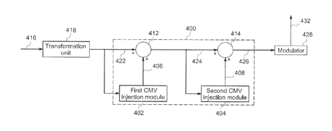
commands 424 provided from the first summation element 412. In the illustrated
embodiment of FIG. 8, the second CMV signal 408 is supplied to a second
summation
unit 414 which combines the second CMV signal 408 with the first modified
three-phase
voltage commands 424 and provides second modified voltage commands 426 In the
illustrated embodiment of FIG. 8, the second modified voltage commands 426 are
supplied to a modulator 428 which is configured to generate control signals
432 for
turning on and off the various switching devices in the second converter 126
to allow the
at least one first function and the at least one second function to be
achieved.
[0050] FIG. 9 is a block diagram illustrating detailed structures of a CMV
injection
module 500 in accordance with one exemplary embodiment of the present
disclosure.
The CMV injection module 500 may be implemented as the second CMV module 404
shown in FIG. 8 for making further modification to the one or more voltage
commands
424 that has been modified by the first CMV signal 406. In the illustrated
embodiment of
FIG. 9, the CMV injection module 500 includes a min-max classifier 506, a CMV
limit
calculator 518, a neutral point (NP) current calculator 528, a NP current pre-
calculator
544, a reference NP current calculator 556, an inverse function calculator
562, and a DC
voltage balance regulator 582.
CA 02911829 2015-11-12
275537
[0051] In one embodiment, the min-max classifier 506 is configured to
receive
voltage commands such as three-phase voltage commands 504. The min-max
classifier
506 is further configured to identify a maximum voltage command 508 and a
minimum
voltage command 512 at any instant from the three-phase voltage commands 504.
In
some embodiments, the min-max classifier 506 may be further configured to
identify a
medium voltage command 509 at any instant from the three-phase voltage
commands
504. The min-max classifier may compute the maximum voltage command 508, the
medium voltage command 509, and a minimum voltage command 512 based on the
following equations:
Umax = MaX(U a* , Ub* , , Umid = mid(Ua*, Ub*, Umin = min(Ua*, Ub*, U,*)
where Uma, is an instantaneous maximum voltage, Umid is an instantaneous
medium
voltage and Uniiõ is an instantaneous minimum voltage, U, Ub*, Uc* are
instantaneous
voltages as phase a, phase b and phase c respectively.
[0052] The same min-max classifier 506, or in some embodiments a different
min-
max classifier may be configured to receive three-phase current commands 502
and
identify a current command 516 corresponding to the maximum voltage command
508, a
current command 514 corresponding to the minimum voltage 512, and a current
command 515 corresponding to a medium voltage 509 at any instant from the
three-phase
current commands 502. The instantaneous maximum voltage 508 the instantaneous
minimum voltage 512 and the instantaneous medium voltage 509 are supplied to
the
CMV limit calculator 518 which is configured to calculate a maximum CMV limit
524
and a minimum CMV limit 526 according to one or more criteria. In one
particular
embodiment, the CMV limit calculator 518 generates the maximum and minimum CMV
limits 524, 526 based on a three-level CMV limit signal 522. In one
embodiment, the
three-level CMV limit may be computed based on a three-level carrier band
voltage.
Either the maximum CMV limit 524 or the minimum CMV limit 526 is set to ensure
that
the modified voltage command signal does not exceed or fall below an original
three
level carrier band voltage. In some embodiments, either or both the maximum
and
21
CA 02911829 2015-11-12
275537
minimum CMV limits 524, 526 are set to ensure the one or more voltage commands
after
CMV injection does not change signs (e.g., from positive to negative or from
negative to
positive).
when Undd> 0,
cm_max = min(1 Umax, 1 ¨ Unrid, 0 ¨ Uiniii), and
Ucmnin = max(0 ¨ Urnõ,, 0 ¨ Umid, ¨1 ¨ Umin)
Similarly, when Umid< 0,
cm_max = min(1 Umax,0 ¨ Urnid, 0 ¨ Urnin), and
Ucm_min = max(0 ¨ Umax, ¨1 ¨ Umid, ¨1 ¨ Urnin)
where //cm_rna, is the maximum common mode voltage limit and U cminin is the
minimum common mode voltage limit.
[00531 In another embodiment, the three-level CMV limit may be computed
based on
a three-level carrier band voltage as discussed above; however, the medium
voltage
command 509 may change the sign after the CMV injection. Thus, there is no
limitation
on CMV to maintain the carrier band of the medium voltage command 509.
[0054] In one embodiment, the maximum CMV limit 524 and the minimum CMV
limit 526 are supplied to the NP current calculator 528 which is configured to
calculate
NP current signals after CMV injection based at least in part on the maximum
and
minimum CMV limits 524, 526, and the three phase current 502. The calculation
of the
NP current signals after CMV injection could be done online or offline.
[0055] In other embodiments, the NP current calculator 528 may calculate
the
maximum NP current 538 and the minimum NP current 542 in an analytical manner.
For
example, one or more linear equations may be used for calculation of the
maximum and
minimum NP current signals 538, 542. In one embodiment, the maximum and
minimum
NP current limits 538, 542 are calculated based at least in part on the
maximum CM limit
524, the minimum CM limit 526, and three-phase current commands 502. In other
22
CA 02911829 2015-11-12
275537
embodiments, instead of using the three-phase current commands 502 for
calculation, the
NP current calculator 528 may calculate the maximum NP current 538 and the
minimum
NP current 542 based at least in part on the maximum CM limit 524, the minimum
CM
limit 526, and three-phase feedback current signals 532 (shown in dashed line)
measured
with one or more current sensors at the output of the second converter 126.
Assuming
that a common mode current i(Ucm)may be represented as:
Umõ, + Ucm) U + Uc
i (lion) = (1 _______________ tumax ( 1 _______ in tumid
17tr i Vtri
U U1\
+ (1 Iumin
Vtri
where Ucn, represents a common mode voltage, Vtri represents a carrier band
voltage,
iumax iumid' umin represent an instantaneous current corresponding to the
maximum
voltage command, medium voltage command, and minimum voltage command
respectively.
[0056] As already
discussed above, in embodiments where the one or more voltage
commands do not change signs after the CMV injection, a relationship between
the
neutral point current and the common mode voltage can be represented as a
linear
relationship. However, in embodiments, where the one or more voltage commands
change signs after the CMV injection, a relationship between the neutral point
current
and the common mode voltage can be represented as a non-linear relationship
which has
more than two characteristic points.
[0057] Based on
the above equation, the maximum neutral point current limit
(iõp_max) and the minimum neutral point current limit (inpinin) may be
determined.
The common mode voltage Ucin may include a maximum common mode voltage limit
represented by and a
minimum common mode voltage limit (1/cm_miõ). In
situations where the i(Uõ,_max) > i(Ucnunin), the maximum neutral point
current limit
(inp_mõ ) may be represented as:
23
CA 02911829 2015-11-12
275537
Umax Ucm_max . Umid Ucm max
inp_max = (1 _________________ tumax + (11 _ ) tumid
lItri Vtri
Umin Ucmmax) .
+1( _ tumi
Vtri
where the common mode voltage at the maximum neutral point current represented
by
Ucminp_max will be equal to the maximum common mode voltage limit
[0058] Similarly,
for i(Ucni_.) > i(U,inin), the minimum neutral point current
limit (inp_miõ) may be represented as:
Umax Ucm_min) Umid Ucmmin ;
inp_min = 1 ___________________ tumax (II 1) tumid
Vtri li _
tri
(Umin Ucmmin) .
+1 _
tumin
Vtri
where the common mode voltage at the minimum neutral point current represented
by
Ucminpinin õ will be equal to the
minimum common mode voltage limit Uc,,,iõ
_.
[0059]
Alternatively, the i(Ucm_max) < i(Ucni_min), the maximum neutral point
current limit(inp_max) may be represented as:
= (1 Umax Ucm_min); (1 Umid Ucm_minl) .
inp_max _______________________ tumax tumid
Vtri 1/tri
Umin Ucmmin) .
+1( _ tumin
Vtrt
where the common mode voltage at the maximum neutral point current represented
by
Ucminp_max will be equal to the minimum common mode voltage limit Ucm_min.
24
CA 02911829 2015-11-12
275537
[0060] Similarly, for i(Ucm_max) < i(U,,,_miii), the minimum neutral point
current
limiti
(-np_min) may be represented as:
Umax U cm_max Umid Ucmm_ax
inp_min (1 tumax + (11 1) tumid
Vtri Vtri
Umin Ucm max".
+(\1_luin
Vtri
where the common mode voltage at the minimum neutral point current represented
by
Ucminp _min will be equal to the maximum common mode voltage limit Ucm_max.
[0061] In embodiments, where the relationship between the neutral point
current and
the common mode voltage is non-linear having more than two characteristic
points, the
neutral point current is computed separately in different sections.
[0062] Further referring to FIG. 9, the maximum NP current limit 538 and
the
minimum NP current limit 542 are supplied to the reference NP current
calculator 556
which is configured to calculate a reference NP current 558 represented by (i)
based at
least in part on a pre-calculated NP current 554, a gain signal 584, and the
maximum and
minimum NP current limit signals 538, 542. The reference NP current calculator
receives
the pre-calculated NP current 554 from an NP current pre-calculator 544.
[0063] In one embodiment, the pre-calculated NP current 554 is calculated
by the NP
current pre-calculator 544 based at least in part on the instantaneous
maximum, medium,
and minimum voltage commands 508, 509, 512 and instantaneous maximum, medium,
and minimum current commands 516, 515, 514. More specifically, in one
embodiment,
the NP current pre-calculator 544 may calculates the pre-calculated NP current
554 using
the following equation:
Umax 0\ / Umid + 0 ) Umin + 0)
tilPpre
= (1 tumax + tumid + (1
tumin
Vtri Vtri Vtri
CA 02911829 2015-11-12
275537
[0064] Furthermore, the reference NP current calculator 556 calculates the
reference
NP current 558 based on the following equations:
in*p = in*p_pre (1 ¨ 9cm) inp_max X gcm for gcn,> 0
tnp ¨ tnp_pre for gc,, = 0
in*p = p_pre(1 gcm) inp_min X gcm for gcn, < 0
where 1p pre represents a pre-calculated NP current and gm represents a common
mode
gain.
[0065] In one embodiment, the gain signal 584 is generated from a DC
voltage
balance regulator 582 which may be a proportional-integral (PI) regulator or
any other
similar regulator. The DC voltage balance regulator 582 receives a voltage
error signal
578 which is generated from a summation element 576 by subtracting a DC
voltage
difference signal 574 from a zero DC voltage command signal 572. The DC
voltage
difference signal 574 represents a voltage difference between the first
capacitor 242 and
the second capacitor 244 of the DC link 270 of FIG. 2 and FIG. 3. The zero DC
voltage
command signal 572 is set to indicate that the desired DC voltage difference
between the
two capacitors should be zero.
[0066] With continuing reference to FIG. 9, the reference NP current signal
558
calculated with the reference NP current calculator 556 is further supplied to
the inverse
function calculator 562. The inverse function calculator 562 is configured to
calculate a
CMV signal 564 based at least in part on the reference NP current signal 558,
maximum
and minimum NP current limits 538, 542, and the first and second CMV voltage
534, 536
corresponding to the maximum and minimum NP current limits 538, 542. In one
embodiment, the inverse function calculator 562 may use one or more linear
equations
defined between the neutral point current and the common mode voltage for
calculation
of the desired CMV signal 564. One such equation may be represented as:
in*pinp_min
Uon = Ucminp_771171 . X (Ucminp max ¨ Ucminp_min)
L'np_max inp_min
26
CA 02911829 2015-11-12
275537
[0067] In other embodiments, the inverse function calculator 562 may obtain
the
CMV signal be referring to a lookup table. The CMV signal 564 is supplied to a
summation element 566 which provides one or more modified voltage command
signals
or modulation signals 568 by combining the CMV signal 564 with the one or more
voltage command signals 504. The one or more modified voltage command signals
or
modulation signals 568 are supplied to the modulator 428 shown in FIG. 8 to
achieve the
function of balancing the DC voltages at the DC capacitors 242, 244 of the DC
link 270.
[0068] FIG. 10 is an exemplary graphical representation 610 depicting a
three level
CMV limit 522 (FIG. 11) as applied to a three-level converter in accordance
with an
embodiment of the invention. The representation 610 depicts two three-level
carrier
waves 612 and 614. The two three-level carrier waves 612 and 614 are located
within
two three-level carrier band voltages 616 and 618 respectively. The carrier
band voltage
616 is defined by a first voltage level 620 and a second voltage level 622.
Similarly, the
carrier band voltage 618 is defined by the second voltage level 622 and the
third voltage
level 624. As shown in schematic representation 610, a maximum CMV limit for a
reference voltage 625 in the carrier band 616 in the three-level converter is
represented
by arrows 626, 628 at time instants T1 and T2 respectively. At time instant
Ti, a
maximum CMV limit is equal to a subtraction between the first voltage level
620 and the
reference voltage level 627, which is a positive number; and the minimum CMV
limit is
equal to a subtraction between the second voltage level 622 and the reference
voltage
level 627, which is a negative number. At time instant T2, the maximum CMV
limit is
equal to a subtraction between the voltage level 620 and the reference voltage
level 629;
the minimum CMV limit is equal to a subtraction between the reference voltage
level 629
and the second voltage level 622. Similarly, the maximum CMV limit for the
reference
voltage 625 at this carrier band 618 is equal to the distance between the
second voltage
level 622 and the reference voltage level 627, 629 at each time instant; the
minimum
CMV limit for the reference voltage 625 at this carrier band 618 is equal to
the distance
between the third voltage level 624 and the reference voltage level 627, 629
at each time
instant. The sign for the maximum CMV limit is positive and the sign for the
minimum
27
CA 02911829 2015-11-12
275537
CMV limit is negative. The final maximum CMV limit for the three phase system
will be
the minimum value out of the three maximum CMV limits for the three phase
respectively; and the final minimum CMV limit for the three phase system will
be the
maximum value out of the three minimum CMV limits for the three phase
respectively.
[0069] FIG. 11 is an exemplary graphical representation 630 depicting a
three level
CMV limit as applied to a five-level converter in accordance with an
embodiment of the
invention. For a five-level converter, the representation 630 depicts four
five-level
carrier waves 632, 634, 636, 638. The four five-level carrier waves 632, 634,
636, 638
are located within four five-level carrier band voltages 640, 642, 644, 646
respectively.
The carrier band voltage 640 is defined by the first voltage level 620 (FIG.
8) and a
fourth voltage level 648. The carrier band voltage 642 is defined by the
fourth voltage
level 648 and the second voltage level 622 (FIG. 8). Similarly, the carrier
band voltage
644 is defined by the second voltage level 622 and a fifth voltage level 650,
and the
carrier band voltage 646 is defined by the fifth voltage level 650 and the
third voltage
level 624 (FIG. 8). Furthermore, the maximum CMV limit and the minimum CMV
limit
for the five-level converter is represented by arrows 652, 654 at time
instants Ti and T2
respectively. As can be seen, the CMV limit for the five-level converter at
carrier band
640 and 642 and are thus equal to the CMV limit for the three-level converter
at carrier
band 616. Therefore, the same three-level CMV limit can be applied to the five-
level
converter.
[0070] FIG. 12 is an exemplary graphical representation 660 depicting a
three level
CMV limit as applied to a seven-level converter in accordance with an
embodiment of
the invention. For a seven-level converter, the representation 660 depicts six
seven-level
carrier waves 662, 664, 666, 668, 670, 672. The six seven-level carrier waves
662, 664,
666, 668, 670, 672 are located within six seven-level carrier band voltages
674, 676, 678,
680, 682, 684 respectively. The carrier band voltage 674 is defined by the
first voltage
level 620 (FIG. 8) and a fourth voltage level 686. The carrier band voltage
676 is defined
by the fourth voltage level 686 and the fifth voltage level 688. The carrier
band voltage
28
CA 02911829 2015-11-12
275537
678 is defined by the fifth voltage level 688 and the second voltage level 622
(FIG. 8).
Similarly, the carrier band voltages 680, 682 and 684 may be defined by a
sixth voltage
level 690, a seventh voltage level 692 and the third voltage level (FIG. 8).
The maximum
CMV limit and the minimum CMV limit for the five-level converter is
represented by
arrows 694, 696 at time instants Ti and T2 respectively. As can be seen, the
CMV limit
for the seven-level converter at carrier band 674, 676, 678 and are thus equal
to the CMV
limit for the three-level converter at carrier band 616. Therefore, the same
three-level
CMV limit can be applied to the seven-level converter. Similarly, the three-
level CMV
limit can be applied for an n-level converter to determine the common mode
voltage for
injection.
[0071] Further referring to FIGs. 10-12, in some embodiments, applying the
three-
level CMV limit to three-phase voltage commands at any instant may generate
three
different maximum CMV limits and three different minimum CMV limits. In this
case,
the maximum CMV limit 524 may be the one that is a minimum of the three
different
maximum CMV limits, and the minimum CMV limit 526 is the one that is a maximum
of
the three different minimum CMV limits. It can be understood that using the
three-level
CMV limit to represent the maximum and minimum CMV limits for an n-level
converter
can avoid complexity in computations for controlling the switching of the
power
converters.
[0072] FIG. 13 is a flowchart illustrating a common mode voltage injection
method
800 in accordance with one exemplary embodiment of the present disclosure. The
CMV
injection method 800 may be independently implemented by the second CMV
injection
module 404 shown in FIGS. 8-9 to achieve at least one function of balancing DC
voltage
present at a DC link of the power conversion system 100. The common mode
voltage
injection method 800 may also be implemented in combination with the first CMV
injection module 402 to achieve multiple functions in association with the
operation of
the power conversion system 100. At least some of the blocks/actions
illustrated in
method 800 may be programmed with software instructions stored in a computer-
29
CA 02911829 2015-11-12
275537
readable storage medium. The computer-readable storage medium may include
volatile
and nonvolatile, removable and non-removable media implemented in any method
or
technology. The computer-readable storage medium includes, but is not limited
to,
RAM, ROM, EEPROM, flash memory or other memory technology, CD-ROM, digital
versatile disks (DVD) or other optical storage, magnetic cassettes, magnetic
tape,
magnetic disk storage or other magnetic storage devices, or any other non-
transitory
medium which can be used to store the desired information and which can be
accessed by
one or more processors.
[0073] In one embodiment, the method 800 may include a block 802, in which
one or
more voltage commands such as three-phase AC voltage commands are obtained. In
one
embodiment, the one or more voltage commands or the three-phase AC voltage
commands may be obtained from one or more upper level controllers by
implementing
one or more algorithms to achieve a desired AC voltage at the output of the
power
converter. In one embodiment, the one or more voltage commands may be signals
that
are free of CMV injection. In other embodiments, the one or more voltage
commands
may have already been modified by a first CMV signal which may be generated
through
min-max calculation or has pure third-order harmonic signal as described above
with
reference to FIG. 8.
[0074] At block 804, the method 800 continues to classify the obtained one
or more
voltage commands. For example, a min-max classifier 506 (see FIG. 11) may be
used to
identify at least a maximum value and a minimum value from the one or more
voltage
commands at each instantaneous time. In some embodiments, a medium voltage may
also be identified using the min-max classifier 506.
[0075] At block 806, the method 800 continues to calculate a maximum CM
voltage
limit and a minimum CM voltage limit based at least in part on the
instantaneous
maximum and minimum voltage commands using a three-level CMV limit. At block
808, the method 800 continues to calculate NP current signals after CMV
injection based
on the maximum CMV limit and the minimum CMV limits. The calculation of the NP
CA 02911829 2015-11-12
275537
current signals can be done in analytical manner. In one embodiment, the
calculation of
the NP current signals are based on all characteristic points in the non-
linear relationship
between the NP current and the common mode voltage including the maximum and
minimum CMV limits.
[0076] At block 810, the method SOO continues to calculate a reference NP
current
based at least in part on a pre-calculated NP current, the maximum and minimum
NP
current limits, and a gain signal. In some embodiments, the gain signal is
generated by a
DC link voltage balance controller by regulating input signals representing
voltage
difference between at least two DC capacitors of the DC link.
[0077] At block 812, the method 800 continues to calculate a CMV injection
signal
based at least in part on the calculated reference NP current. In one
embodiment, a
reverse function such as one or more linear functions of the CM voltage in
terms of NP
current can be derived for calculation of the CMV injection signals. At block
814, the
one or more voltage commands obtained at block 802 is modified by combining
the
reference CMV injection signal with the one or more voltage commands. In some
embodiments, the modified one or more voltage commands are supplied to a
modulator
for generating control signals used to turn on and/or off the various
switching devices in
the power converter. Therefore, the voltage difference at the DC link can be
minimized
by injecting the CMV signals to the one or more voltage commands or modulation
signals.
[0078] The method 800 described above with reference to FIG. 13 may be
modified
in a variety of ways. For example, in some embodiments, the method 800 may
include
additional one or more blocks/actions. For example, the method 800 may include
blocks
for obtaining one or more current commands which are used to calculate the
original NP
current at the neutral point of the DC link. The method 800 may also include
blocks for
identifying at least an instantaneous current at maximum voltage and an
instantaneous
current at minimum voltage from one or more current commands.
31
CA 02911829 2015-11-12
275537
[0079] While the
invention has been described with reference to exemplary
embodiments, it will be understood by those skilled in the art that various
changes may
be made and equivalents may be substituted for elements thereof without
departing from
the scope of the invention.
Furthermore, the skilled artisan will recognize the
interchangeability of various features from different embodiments. Similarly,
the various
method steps and features described, as well as other known equivalents for
each such
methods and feature, can be mixed and matched by one of ordinary skill in this
art to
construct additional assemblies and techniques in accordance with principles
of this
disclosure. In addition, many modifications may be made to adapt a particular
situation
or material to the teachings of the invention without departing from the
essential scope
thereof. Therefore, it is intended that the invention not be limited to the
particular
embodiment disclosed as the best mode contemplated for carrying out this
invention, but
that the invention will include all embodiments falling within the scope of
the appended
claims.
32