Note: Descriptions are shown in the official language in which they were submitted.
CA 02912192 2015-11-09
WO 2015/038687
PCT/US2014/055047
1
ANODIC BONDING OF THERMALLY STABLE POLYCRYSTALLINE
MATERIALS TO SUBSTRATE
Technical Field
[0001] The present disclosure relates generally to cutting elements and
other
downhole drilling components that include thermally stable polycrystalline
materials
usable in connection with wellbore drilling and systems and methods of
manufacture
using anodic bonding.
Background
[0002] Rotary drill bits are frequently used to drill oil and gas wells,
geothermal
wells, and water wells. Fixed cutter drill bits or drag bits are often formed
with a bit
body having cutting elements or inserts disposed at select locations of
exterior
portions of the bit body. Drill bits and other downhole equipment may also
have a
variety of other abrasive and/or wear-resistant, hardfacing elements. Cutting
elements and hardfacing elements can be made from polycrystalline materials.
[0003] For example, cutting elements having a polycrystalline cutting
layer (or
table) have been used in industrial applications including wellbore drilling
and metal
machining for many years. One such material is a polycrystalline diamond
(PCD),
which is a polycrystalline mass of diamonds (typically synthetic) that is
bonded
together to form an integral, tough, high-strength mass. To form a cutting
element, a
cutting layer is bonded to a substrate material, which is typically a sintered
metal-
carbide. When bonded to a substrate, a POD is referred to as a polycrystalline
diamond compact (PDC). Polycrystalline materials for use in cutting elements
or
hardfacing structural elements can also be made from other polycrystallline
materials
such as polycrystalline cubic boron nitride (PCBN).
CA 02912192 2015-11-09
WO 2015/038687
PCT/US2014/055047
2
[0004] Methods for securing thermally stable polycrystalline material to a
substrate for use in drill bit cutting element, or other abrasive and/or wear-
resistant,
hardfacing structural element that are part of a drill bit body or other
downhole
equipment have been actively investigated. High temperature high pressure
(HTHP)
processing is a common method of attachment. However, this method typically
uses
another catalyst, such as cobalt, and results in reduced thermal stability of
the
polycrystalline material.
Brief Description of the Drawings
[0005] FIG. 1 is a perspective view of a drill bit containing cutting
elements
according to one embodiment.
[0006] FIG. 2 is perspective view of a cutting element having a cutting
layer of
thermally stable polycrystalline material attached to a substrate according to
one
embodiment.
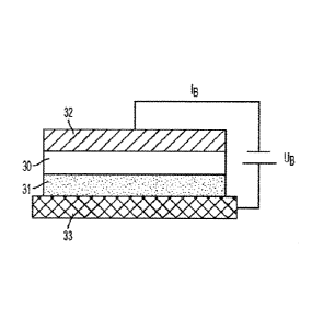
[0007] FIG. 3A is a schematic illustrating the components for performing
an
anodic bonding procedure. Some process parameters are bond voltage (UB),
current limitation (IB), and bond temperature (TB).
[0008] FIG. 3B is a schematic illustrating the ionic drift associated with
the
anodic bonding process of FIG. 3A.
[0009] FIG. 4A is a schematic showing the ionic drift associated with anodic
bonding
of carbonate-containing thermally stable polycrystalline material to a
substrate
according to one embodiment.
[00010] FIG. 4B is a schematic showing the ionic drift associated with
bonding
of carbonate-containing thermally stable polycrystalline to silicon-coated
substrate
according to one embodiment.
CA 02912192 2015-11-09
WO 2015/038687
PCT/US2014/055047
3
[00011] FIG. 5 is a schematic of a system for bonding a cutting layer of
thermally stable polycrystalline material to a substrate to form a cutting
element
according to one embodiment.
[00012] FIG. 6 is a block diagram of a method of making a cutting element
having a cutting layer of thermally stable polycrystalline material attached
to a
substrate according to one embodiment.
Detailed Description
[00013] Certain embodiments and features of the present disclosure relate
to
cutting elements and hardfacing components of drill bits and other downhole
equipment that include thermally stable polycrystalline material and can be
used in
connection with wellbore drilling and systems, as well as methods of
manufacturing
such elements using anodic bonding. In some examples, a cutting element having
a
thermally stable polycrystalline material cutting layer can be attached to a
drill bit
head or other downhole equipment, such as a reamer or a hole opener, that can
be
used to break apart, cut, or crush rock and earth formations when drilling a
wellbore,
such as those drilled to extract water, gas, or oil. In another example, a
hardfacing
component having a thermally stable polycrystalline material outer-facing
layer can
be attached to a drill bit or other downhole equipment. Such hardfacing
components
may be wear-resistant, reducing susceptibility of the drill bit or downhole
equipment
to damage due to frictional heat and may facilitate movement of the equipment
downhole during use. Examples of hardfacing components include drill bit
heads,
gage protectors, and impact arrestors. An electrical field can be used to
covalently
bond the thermally stable polycrystalline material to a substrate to form the
cutting
element or hardfacing component. In some examples, anodic bonding of the
thermally stable polycrystalline material to the substrate or hardfacing
component
CA 02912192 2015-11-09
WO 2015/038687
PCMJS2014/055047
4
maximizes the thermal stability of the cutting element or hardfacing
component. As
a result, the cutting element or hardfacing component can have improved
therrno-
mechanical integrity and abrasion resistance, and has reduced leaching
exposure
compared to those made using conventional methods of attaching a cutting layer
to
a substrate.
[00014] A PCD includes individual diamond "crystals" that are
interconnected in
a lattice structure. A metal catalyst (in particular, Group VIII metal
catalysts), such
as cobalt, has been used to promote recrystallization of the diamond particles
and
formation of the lattice structure (for example, in a sintering process).
However,
Group VIII metal catalysts have significantly different coefficient of thermal
expansion
(CTE) as compared to diamond and, upon heating a PCD, the metal catalyst and
the
diamond lattice will expand at different rates, causing cracks to form in the
lattice
structure and resulting in deterioration of the cutting layer (during downhole
use).
Also, at elevated temperatures (>800 C) and in the absence of elevated
pressure,
the metal catalyst will also revert the diamond to graphite. In order to
obviate this
problem, strong acids may be used to "leach" the cobalt from the diamond
lattice
structure, generating a thermally stable polycrystalline diamond material.
Similar
issues occur and must be addressed for other polycrystalline materials.
Cutting
elements with a cutting layer of thermally stable polycrystalline material
have
relatively low wear rates, even as cutter temperatures reach 1200 C.
[00015] In some cases, the polycrystalline material is made of diamond or
other
superhard particles bound together with a binder (for example, silicon) in a
matrix
composite. Hardfacing components may include this type of polycrystalline
material
as an abrasive and/or wear-resistant feature.
CA 02912192 2015-11-09
-
WO 2015/038687
PCT/US2014/055047
_
[00016] For simplicity, features of a drill bit cutting element
that includes a
thermally stable polycrystalline material cutting layer made from a
polycrystalline
diamond (PCD), along with systems and methods for making and using this
component, are described in detail. However, such features similarly relate to
abrasive or wear-bearing hardfacing components of a drill bit or other
downhole
equipment, along with systems and methods for making and using such
components. Such features also similarly relate to components containing other
polycrystalline materials, along with systems and methods for making and using
such components.
[00017] In one example, a cutting element that includes a
cutting layer made of
thermally stable polycrystalline material anodically bonded to a substrate is
attached
to a drill bit for earth formation drilling. A fixed cutter drill bit 10
having such cutting
elements is shown in FIG. 1. The bit head 11 is connected to a shank 12 to
form a
bit body 13. A plurality of cutter blades 14 are arranged around the
circumference of
the bit head 11. In this example, there are five cutter blades 14 that extend
generally
outwardly away from a rotational axis 15 of the drill bit. Pockets or recesses
16,
otherwise called sockets and receptacles, are formed on the cutter blades 14.
Cutting elements 17, otherwise known as inserts, are fixedly installed in each
pocket
16, for example by brazing. A plurality of cutting elements 17 are disposed
side by
side along the length of each blade. The number of cutting elements 17 carried
by
each blade may vary. As the drill bit 10 is rotated in use, it is the cutting
elements 17
that come into contact with the formation, in order to dig, scrape or gouge
away the
material of the formation being drilled. Gage protectors 18 are located on the
outward-facing surface of the plurality of cutter blades 14, where they
facilitate
rotation of the bit body 13 and provide wear resistance.
CA 02912192 2015-11-09
-
WO 2015/038687
PCT/US2014/055047
_
6
[00018] In another example, a cutting element 20 that includes a
thermally
stable polycrystalline material anodically bonded to a substrate is shown in
FIG. 2.
The cutting element 20 has a cylindrical substrate body (substrate) 22 having
an end
face or upper surface 23 referred to herein as the interface surface 23. An
ultra-hard
material layer (cutting layer) 24 forms the working surface 25 and the cutting
edge
26. A bottom surface 27 of the cutting layer 24 is anodically bonded on to the
upper
surface 23 of the substrate 22. The joining surfaces 23 and 27 are herein
referred to
as the interface 28. The interface 28 is where surface 23 of the substrate 22
are
covalently attached to each other by anodic bonding. The top exposed surface
or
working surface 25 of the cutting layer 24 is opposite the bottom surface 27.
The
cutting layer 24 typically may have a flat or planar working surface 25, or a
non-
planar surface (not shown separately).
[00019] For example, the cutting layer 24 can include a
thermally stable
polycrystalline material. The thermally stable polycrystalline material may
include
polycrystalline diamond, polycrystalline cubic boron nitride, or another super
abrasive material. The substrate 22 may be a carbide or a metal. For example,
the
carbide may include cemented tungsten carbide (WC), silicon carbide (SiC), or
another super hard material. Where the substrate 22 is a metal, the metal may
include steel, a nickel/iron alloy, Invar, or titanium. Examples of substrates
include
metals (for example, steel, invar, titanium, etc.), silicon-coated metals,
silicon-coated
and cemented tungsten carbide, and silicon carbide. Either or both of the
cutting
layer 24 and the substrate 22 can be plated, layered, or coated with metal or
silicon
to facilitate the anodic bonding process. In some examples, the substrate 22
may be
a carbide or a metal that includes, or is covalently coated with, silicon.
CA 02912192 2015-11-09
WO 2015/038687
PCT/US2014/055047
7
[00020] The cutting layer 24 may be anodically bonded to the substrate 22
directly or may be anodically bonded to an interlayer that is bonded to the
substrate
22. In certain examples, the cutting layer 24 may be bonded to the substrate
22
indirectly via an interlayer (FIG. 2, not shown). The upper surface of the
interlayer
can be anodically bonded to the bottom surface 27 of the cutting layer 24. The
interlayer may be substance that forms a carbide that can be bonded to a
polycrystalline material of the cutting layer 24. For example, the interlayer
may be a
metal, such as steel, a nickel/iron alloy, Inver, or titanium. The interlayer
may be
made of multiple substances that have different affinities for each other, for
the
substrate 22, and for the polycrystalline material. The interlayer may also be
multiple
layers of different substances that have different affinities for each other,
for the
substrate, and for the polycrystalline material of the cutting layer 24. In
some
examples, the interlayer may be a metal covalently coated with silicon. The
metal of
the interlayer may be ductile to absorb residual stresses from both the anodic
bonding process as well as, for example, the brazing process that may be used
to
bond the thermally stable polycrystalline material-interlayer to the substrate
22.
Residual thermal stress can be managed by a single interlayer or multiple
interlayers.
[00021] A drill bit 10 as shown in Fig. 1 may be made using anodic bonding
to
attach the cutting layer 24 to the substrate 22 or the interlayer. Anodic
bonding can
be used to covalently bond a first material 30 to a second material 31, as
shown in
FIG. 3A. The first material 30 and the second material 31 are placed adjacent
to
each other and positioned between a cathode 32 and an anode 33. An
electrostatic
field is generated by applying an electrical current to the anode that can
attract or
repel positive and negative charged ions present in the first material 30 or
the
CA 02912192 2015-11-09
WO 2015/038687
PCMJS2014/055047
8
second material 31 to generate a covalent bond between the two materials. As
the
first material and second material are solid, the ion drift generated by the
electrostatic field occurs at the surface of the two materials to facilitate
their covalent
bonding. In some examples, the anode and the cathode further include heating
elements for applying heat to the first material and the second material to
facilitate
anodic bonding. The anodic bonding process may be performed inside a
temperature-controlled environment. Parameters of the anodic bonding process
include bond voltage (Us), current limitation (16), bond temperature (TB), as
well as
contact pressure and time.
[00022] For example, anodic bonding has been used to covalently bond glass
to a second material such as silicon, metal, or other materials. In this
context,
anodic bonding can involve positioning a first material 30, such as glass, and
a
second material 31, such as silicon, in atomic contact through an
electrostatic field.
The electrostatic field can attract or repel positive and negative charged
ions present
in the glass as shown in FIG. 3B. The glass can include a high concentration
of
alkali or alkaline ions (for example, Na2+). The positively charged ions drift
toward
the cathode, forming a "depletion zone" at the glass surface adjacent to the
second
material 31, while the negatively charged ions drift into the depletion zone
toward the
interface 34 between the glass surface and the second material. At the
interface 34,
the negative charged ions (such as oxygen) can react with the second material
(for
example, silicon) to form a covalent oxide bonding layer (such as, silicon
oxide).
[00023] In using anodic bonding as a mechanism for attaching a thermally
stable polycrystalline material cutting layer to a substrate for use in a
drill bit, the
characteristics of the thermally stable polycrystalline material and the
substrate (and
the interlayer, if included) should be considered.
CA 02912192 2015-11-09
WO 2015/038687
PCT/US2014/055047
9
[00024] For example, a factor in selecting the thermally stable
polycrystalline
material, the substrate, and the interlayer (or interlayers) can be the
coefficient of
thermal expansion (CIE) of each. CIE is the fractional increase in the length
per
unit rise in temperature for a material. The differential in GTE between the
substrate
and the thermally stable polycrystalline material may result in thermal
residual stress,
which can cause the thermally stable polycrystalline material to crack upon
being
cooled. To minimize problems caused by thermal residual stress, the CTE of the
thermally stable polycrystalline material may be similar to that of the
substrate or to
the interlayer if an interlayer is used.
[00025] A glass or alkali or alkaline can be added to the thermally stable
polycrystalline material (which does not typically contain glass or such ions)
either
during the pressing process or post pressing to facilitate anodic bonding to a
substrate. For example, typical crystallization Group VIII metal catalysts,
such as
cobalt and nickel, can be replaced with a carbonate catalyst. Carbonate
catalysts
can provide the ions utilized for anodic bonding. Examples of such carbonate
catalysts include magnesium carbonate (MgCO3), silicon carbonate (SiC0),
sodium
carbonate (Na2CO3), potassium carbonate (K2CO3), strontium carbonate (SrCO3),
calcium carbonate (Ca2CO3), and lithium carbonate (Li2CO3). In some examples,
multiple carbonate catalysts are used to form the thermally stable
polycrystalline
material. Unlike metal catalysts, carbonate catalysts do not function as a
catalyst
after the press cycle in forming the polycrystalline material. Thus, removal
of the
carbonate catalyst from the polycrystalline material (for example, by
leaching) to
generate a fully thermally stable polycrystalline material is not necessary.
As shown
in FIG. 4A, the negatively charged oxygen ions present in the thermally stable
polycrystalline material may drift into the depletion zone toward the
interface 34
CA 02912192 2015-11-09
WO 2015/038687
PCT/US2014/055047
between the thermally stable polycrystalline material (first material 30) and
the
substrate (second material 31). At the interface 34, the oxygen ions can react
with
the second material to form a covalent oxide bonding layer, thereby covalently
attaching the thermally stable polycrystalline material (first material 30) to
the
substrate (second material 31).
[00026] In some examples, the substrate may be covalently coated with a
layer
of silicon to facilitate the anodic bonding process. As shown in FIG. 4B, the
negatively charged oxygen ions present in the thermally stable polycrystalline
material drift into the depletion zone toward the interface 34 between the
thermally
stable polycrystalline material (first material 30) and the silicon layer on
the substrate
(second material 31). At the interface 34, the oxygen ions can react with the
silicon
to form a covalent silicon oxide bonding layer. The interlayer can then be
attached
to the substrate to form the drill bit (for example, by sintering). More than
one
interlayer 34 may be used to attach the thermally stable polycrystalline
material (first
material 30) to the substrate (second material 31).
[00027] FIG. 5 is a block diagram illustrating systems for making a cutting
element according to certain embodiments. For example, the system 50 includes
an
anode 33, a cathode 32, a first material 30 that is a cutting layer (a
thermally stable
polycrystalline material), and a second material 31 that is a substrate in
contact with
the cutting layer, and a current generator 51. The cutting layer (first
material 30) and
the substrate (second material 31) are disposed between the anode 33 and the
cathode 32, with anode 33 in contact with the cutting layer (first material
30), and the
cathode 32 in contact with the substrate (second material 31). The current
generator
51 sends a current from the anode to the cathode to generate an electric field
52 and
CA 02912192 2015-11-09
WO 2015/038687
PCT/US2014/055047
11
cause anodic bonding between the cutting layer (first material 30) and the
substrate
(second material 31).
[00028] Heating the thermally stable polycrystalline material and the
substrate
(or interlayer), as the electrical current is being delivered to the thermally
stable
polycrystalline material and the substrate, can facilitate the movement of
ions to
improve anodic bonding. The temperature at which the anodic bonding process
occurs influences the amount of time it will take for the bonding to occur. At
cooler
temperatures, the bonding process may proceed slowly, while at warmer
temperatures, the bonding process may occur more quickly. Another factor in
selecting the bonding temperature is the temperature at which the bonds of the
thermally stable polycrystalline layer degrade. The lower the temperature at
which
bonding occurs, the lower the residual stress may be in the bonding layer due
to
geometric changes from the coefficient of thermal expansion (GTE). For
example, a
thermally stable polycrystalline diamond material can have a maximum
temperature
limit of approximately 800-1200 C (depending on atmospheric conditions) at
which
the diamond bonds begin to break down in the thermally stable polycrystalline
material. Thus, in some cases, the temperature selected for the anodic bonding
process is as warm as the thermally stable polycrystalline material can be
heated
with minimal or no degradation. In some examples, the temperature selected for
the
anodic bonding process may be below the temperature at which the bonds of the
thermally stable polycrystalline layer degrade but high enough to increase the
rate at
which the anodic bonding process occurs. In some examples, the anodic bonding
process can involve using relatively low temperatures for bonding. Another
factor
that can increase the rate of the anodic bonding process is the strength of
the
electrostatic field. For example, the strength of the electrostatic field can
be
CA 02912192 2015-11-09
_
WO 2015/038687
PCT/US2014/055047
_
12
increased to encourage movement of ions. Increasing the strength of the
electrostatic field may also cause the thermally stable polycrystalline
material and
the substrate (or interlayer) to heat.
[00029] In some cases, the temperature for the anodic bonding
process may be
much lower than the temperature used to debond the joint. For example, for a
polycrystalline diamond material, an anodic bond may be created, as the
electrical
current is being delivered to the thermally stable polycrystalline material
and the
substrate, at a temperature below 800 C. In some instances, however, the
polycrystalline diamond material may be heated to a temperature at or above
800 C
to debond. In some instances, the anodic bonding temperatures, as the
electrical
current is being delivered to the thermally stable polycrystalline material
and the
substrate, can be increased, for example, to about 1,000 C, to increase
mobility of
ions in the thermally stable polycrystalline material and the substrate. The
anodic
bonding process may be performed such that the thermally stable
polycrystalline
material is heated, as the electrical current is being delivered to the
thermally stable
polycrystalline material and the substrate, to a temperature between about 100
C
and about 900 C, or between about 200 C and about 800 C, or between about
200 C and about 700 C, or between about 200 C and about 600 C, or between
about 400 C and about 800 C, or between about 400 C and about 700 C, or
between about 400 C and about 600 C. For example, the thermally stable
polycrystalline material may be heated, as the electrical current is being
delivered to
the thermally stable polycrystalline material and the substrate, to at least
about 100
C, about 200 C, about 300 C, about 400 C, about 500 C, about 600 C, about
700 C, or about 800 C.
CA 02912192 2015-11-09
WO 2015/038687
PCT/US2014/055047
13
[00030] In some instances, a heating element is used to for apply heat to
the
cutting layer (thermally stable polycrystalline material), the substrate (or
interlayer),
or both the cutting layer and the substrate (or interlayer), to facilitate
anodic bonding.
In certain examples, the cathode 32 and anode 33 may directly provide heat to
the
cutting layer and the substrate (or interlayer) as a result of generating an
electrostatic field. Alternatively, the anodic bonding process may be
performed in an
enclosed compartment for heating (for example, a furnace).
[00031] FIG. 6 is a block diagram illustrating methods for making a cutting
element according to various embodiments. The method 60 shown in FIG. 6 is
described with respect to the environment shown in FIG. 5. In block 61, a
cutting
layer (first material 30; a thermally stable polycrystalline material) is
positioned in
contact with a substrate (second material 31; for example, a carbide). In
block 62,
the cutting layer and the substrate are positioned between an anode 33 and a
cathode 32. Once positioned in the system, the cutting layer is in contact
with the
anode 33, and the substrate is in contact with the cathode 32. Applying the
electrical
current to the anode 33 generates an electrical field 52 between the anode 33
and
the cathode 32 as indicated in block 64. In block 65, the electrical field 52
causes
the cutting layer to be anodically bonded to the substrate, thus forming the
cutting
element. The electrical current is provided by the current generator 51.
[00032] To facilitate positioning of the cutting layer and the substrate
between
them, at least one of the anode and the cathode can be in a fixed position
while the
other is moveable. The anode and the cathode may both moveable. Positioning
the
components of the system may be performed manually or robotically using an
assembly system. The system may include one or more sensors to facilitate
positioning of the various components (not shown). In block 63, an electrical
current
CA 02912192 2015-11-09
WO 2015/038687
PCT/US2014/055047
14
is delivered to the anode once the cutting layer and the substrate are
positioned
between the anode and the cathode.
[00033] In some examples, the method further includes heating the cutting
layer or the substrate when the electrical current is being delivered to the
anode 33.
In certain examples, the anode 33, the cathode 32, or both, include a heating
element. In some cases, the anode 33, the cathode 32, or both, act as a
heating
element that heat the thermally stable polycrystalline material when the
electrical
current is delivered to the anode 33. See, for example, FIG. 5. Alternatively,
the
anodic bonding process can be performed in an enclosed compartment for heating
(such as, for example, a furnace). In some instances, the thermally stable
polycrystalline material is heated to at least 100 C during the bonding
process. In
some examples, the thermally stable polycrystalline material is heated to
temperatures in the ranges described above during the bonding process.
[00034] The features described herein may provide a cutting element or
hardfacing component with improved wear according to one or more of the
following
examples.
[00035] Example 1: A component includes a cutting layer of a substrate and
a
thermally stable polycrystalline material anodically bonded to the substrate.
[00036] Example 2: The component of Example 1 can feature thermally stable
polycrystalline material comprising polycrystalline diamond, or cubic boron
nitride.
[00037] Example 3: The component of any of Examples 1 to 2 can feature
thermally stable polycrystalline material comprising a carbonate.
[00038] Example 4: The component of any of Examples 1 to 3 can feature a
carbonate comprising at least one of magnesium carbonate, silicon carbonate,
CA 02912192 2015-11-09
WO 2015/038687
PCT/US2014/055047
sodium carbonate, potassium carbonate, strontium carbonate, calcium carbonate,
or
lithium carbonate.
[00039] Example 5: The component of any of Examples 1 to 4 can feature
substrate comprising a carbide or a metal.
[00040] Example 6: The component of any of Examples 1 to 5 can feature a
carbide substrate comprising cemented tungsten carbide or silicon carbide.
[00041] Example 7: The component of any of Examples 1 to 6 can feature a
metal substrate comprising steel, a nickel/iron alloy, Invar, or titanium.
[00042] Example 8: The component of any of Examples 1 to 7 can feature a
metal substrate comprising nickel or cobalt.
[00043] Example 9: The component of any of Examples 1 to 8 can feature
carbide substrate or metal substrate comprising silicon, or comprising carbide
or
metal that are covalently coated with silicon.
[00044] Example 10: The component of any of Examples 1 to 9 can feature a
cutting layer that is bonded to the substrate indirectly via an interlayer.
[00045] Example 11: The component of any of Examples 1 to 10 can feature a
cutting layer that is anodically bonded to the interlayer, wherein the
interlayer is
bonded to the substrate.
[00046] Example 12: The component of any of Examples 1 to 11 can feature an
interlayer comprising a metal.
[00047] Example 13: The component of any of Examples 1 to 12 can feature a
metal interlayer comprising steel, a nickel/iron alloy, Invar, or titanium.
[00048] Example 14: The component of any of Examples 1 to 13 can feature a
metal interlayer comprising a metal that is covalently coated with silicon..
CA 02912192 2015-11-09
WO 2015/038687
PCT/US2014/055047
16
[00049] Example 15: The component of any of Examples 1 to 14 can be a
cutting element, a gage protector, an impact arrestor, or other abrasive or
wear-
resistant hardfacing component.
[00050] Example 16: The component of any of Examples 1 to 15 can be
attached to a drill bit, a stabilizer, or a reamer.
[00051] Example 17: A system for making the component of any of Example 1
to 16, such as for making a component, includes an anode, a cathode, the
substrate
in contact with the thermally stable polycrystalline material, and a current
generator
for sending a current from the anode to the cathode. The thermally stable
polycrystalline material and the substrate are disposed between the anode and
the
cathode. The anode is in contact with the thermally stable polycrystalline
material
and the cathode is in contact with the substrate. The current generates an
electric
field and causes anodic bonding between the thermally stable polycrystalline
material and the substrate.
[00052] Example 18: The system of Example 16 can include a heating element
that includes an enclosed compartment for heating and into which the anode,
the
cathode, the substrate, and the thermally stable polycrystalline material are
placed.
[00053] Example 19: The system of Example 16 can include a heating element
that includes one or more heating element components in contact with at least
one of
the anode, the cathode, the substrate, or the thermally stable polycrystalline
material.
[00054] Example 20: A method of making the component according to any of
Examples 1 to 16 includes positioning the thermally stable polycrystalline
material in
contact with a substrate and positioning the thermally stable polycrystalline
material
and the substrate between an anode and a cathode. The thermally stable
CA 02912192 2015-11-09
WO 2015/038687
PCT/US2014/055047
17
polycrystalline material is in contact with the anode, and the substrate is in
contact
with the cathode. An electrical current is delivered to the anode to generate
an
electrical field between the anode and the cathode. The electrical field
causes the
thermally stable polycrystalline material to be anodically bonded to the
substrate.
[00055] The foregoing description of certain embodiments and features,
including illustrated embodiments, has been presented only for the purpose of
illustration and description and is not intended to be exhaustive or to limit
the
disclosure to the precise forms disclosed. Numerous modifications,
adaptations, and
uses thereof will be apparent to those skilled in the art without departing
from the
scope of the disclosure. Certain features that are described in this
specification in
the context of separate embodiments can also be implemented in combination in
a
single implementation. Conversely, various features that are described in the
context of a single implementation can also be implemented in multiple ways
separately or in any suitable subcombination. Moreover, although features may
be
described above as acting in certain combinations, one or more features from a
combination can in some cases be excised from the combination, and the
combination may be directed to a subcombination or variation of a
subcombination.
Thus, particular embodiments have been described. Other embodiments are within
the scope of the disclosure.