Note: Descriptions are shown in the official language in which they were submitted.
CA 02912947 2015-11-19
WO 2014/187926 PCT/EP2014/060591
1
Compact fluid analysis device and method to fabricate
Field of the invention
The present invention relates to the field of biological analysis devices. In
particular, the present invention is related to compact devices for the
analysis of a fluid
sample. More in particular, the present invention is related to fully
integrated lab-on-a-
chip devices for the analysis of fluid samples.
Background of the invention
Currently, state of the art point-of-care devices for the analysis of blood
exist. A
disadvantage of these devices is their size which depends on the different
components
needed to perform analysis of blood. In these devices, external pumps are part
of the
point of care instrument. In some devices, miniature scale pumps are used to
propagate
a sample through the fluidic channels of the device. The use of pumps
increases the
size and cost of the device which makes them less suitable for usage as a
disposable
device. Current disposable devices are typically inserted in expensive read-
out
instruments; with many non-disposable different electronic or optical
components to
read out the biochemical reactions taking place in the disposable. Another
disadvantage of state of the art point of care devices is their cost to
fabricate.
Other state of the art devices are lateral flow test strips. These test strips
are
usually fabricated from cellulose which does not allow a precise control of
the flow of a
fluid sample propagating through the test strips. This narrows the scope of
application
of these devices.
There is a need for a low-cost, easy to use, disposable, compact device for
the
fully integrated analysis of a fluid sample.
Summary of the invention
In a first aspect, the present invention relates to a device for analyzing a
fluid
sample. The device comprises: a fluidic substrate comprising: a micro-fluidic
component embedded in the fluidic substrate configured to propagate a fluid
sample
via capillary force through the micro-fluidic component; and a means for
providing a
fluid sample connected to the micro-fluidic component; a lid attached to the
fluidic
substrate at least partly covering the fluidic substrate and at least partly
closing the
micro-fluidic component. The fluidic substrate is a silicon fluidic substrate
and the lid is
a CMOS chip.
CA 02912947 2015-11-19
WO 2014/187926 PCT/EP2014/060591
2
According to embodiments of the present invention, at least a part of the lid
is in
contact with the fluid sample when the fluid sample is present in the device.
According to embodiments of the present invention, the lid comprises a
transistor
layer, the transistor layer being electrically connected at least one
electrical component,
the electrical component being at least one of the following: biosensing
circuitry,
electrodes for sensing purposes, electrodes for fluid manipulation purposes,
circuitry
for data communication purposes, circuitry for wireless data communication
purposes,
temperature sensors, heater electrodes for temperature control and fluid
sensors and
electrodes for fluidic viscosity control.
According to embodiments of the present invention, the means for providing a
fluid sample is an integrated needle fabricated from silicon and comprising an
inner
fluidic channel connected to the micro-fluidic component The needle is a
protruding
portion of the fluidic substrate and positioned to penetrate skin tissue when
pressed
against the skin tissue.
According to embodiments of the present invention, the fluidic substrate
comprises a cut-out and the needle is positioned in the cut-out.
According to embodiments of the present invention, the fluidic substrate
comprises a protection structure for protecting the needle, removably attached
to the
fluidic substrate.
According to embodiments of the present invention, the means for providing a
fluid sample is an inlet. A sample drop may be inserted into the microfluidic
component
by means of capillary suction. The microfluidic component may comprise
different fluidic
compartments, for instance for muti-omic analysis. The different microfluidic
compartments can have same or different depths. The different microfluidic
compartments may be separated by valves that may be actuated in any suitable
way,
for instance by fluidic forces or by electricity. Electrodes for actuation may
be contained
on the fluidic substrate or on the lid.
According to embodiments of the present invention, the fluidic substrate or
the lid
may further comprise at least one optical waveguide to allow optical
excitation and
sensing of the fluid sample when present in the device. The fluidic substrate
or the lid
may also comprise filters for rejecting optical excitation from emission to
measure a
fluorescent signal. The fluidic substrate or the lid may comprise
multispectral filters for
measuring fluorescent signals with multiple colors. The fluidic substrate or
the lid may
CA 02912947 2015-11-19
WO 2014/187926 PCT/EP2014/060591
3
comprise an optical waveguide and/or a pinhole to irradiate the sample for
performing
lensfree microscopy.
According to embodiments of the present invention, the fluidic substrate or
the lid
comprises at least one through-hole for application of a biochemical reagent
to at least
one region of the micro-fluidic component or to at least one region of the
lid.
According to embodiments of the present invention, the lid is bonded to the
fluidic
substrate using a lithographically patterned polymer.
According to embodiments of the present invention, the device may further
comprise metal contacts electrically connected to the lid for read-out of
electrical signals
generated by the fluid and captured by measurement systems in the lid.
According to
embodiments of the present invention, the lid of the device may further
comprise CMOS
active pixels for readout of optical signals from the fluid.
According to embodiments of the present invention, at least part of the
fluidic
substrate and/or the lid is fabricated from a transparent material to allow
optical
inspection of a fluid sample in the micro-fluidic component.
According to embodiments of the present invention, the shape of the device
allows insertion into a mobile communication device.
In a second aspect, embodiments of the present invention relate to a method
for
fabricating a device for analyzing a fluid sample. The method comprises:
providing a
fluidic substrate; providing a lid; attaching the fluidic substrate to the lid
to close the
fluidic substrate at least partly. The fluidic substrate is a silicon fluidic
substrate and the
lid is CMOS chip; and the fluidic substrate is attached to the lid using a
CMOS
compatible bonding process.
According to embodiments of the present invention, providing a fluidic
substrate
may comprise: providing a silicon substrate, providing a mask layer, for
instance an
oxide mask, patterning the oxide mask so as to create fine structures in the
oxide mask;
providing a protection layer to protect the oxide mask; patterning coarse
structures;
etching of the coarse structures; growing oxide for protecting the coarse
structures;
removing the protection layer and etch the fine structures; removing the
oxide.
According to embodiments of the present invention, providing a fluidic
substrate
may comprise providing a silicon substrate, providing a plurality of masks on
top of one
another and using each mask for creating microfluidic structures of different
depths.
In accordance with particular embodiments of the present invention, providing
a
fluidic substrate may comprise providing a silicon substrate, providing a
first oxide
CA 02912947 2016-06-08
53680-24
4
mask, patterning microfluidic structures, etching the substrate to single
depth, providing
a second oxide mask, patterning microfluidic structures, etching the substrate
to a
second depth, and, if required, repeating these steps for creating multiple
depths of
microfluidic structures.
According to particular embodiments, the fluidic substrate and the lid of a
device
according to embodiments of the present invention may be part of a larger
fluidic
package, which may be made from different materials like for instance
polymers, and
which may contain larger fluidic structures, reagents, fluidic and electrical
interfaces.
The advantage thereof is that such system becomes more cost efficient.
According to embodiments of the present invention, surfaces of the fluidic
substrate and the lid may be partially or fully coated to modify surface
interactions of
the substrate with the fluid sample.
In a third aspect, the present invention provides the use of a device as
described
in the first aspect of the present invention and its embodiments, to perform
microscopy.
Microscopy may be implemented by using the lid for detecting lensfree images
according to the principles of digital holography.
The use of the device as described may perform multi-omic analysis in which
the
fluidic substrate is used for performing multiple assays in multiple channels
and
chambers, and the CMOS lid is used to detect multiple signals from all assays.
Those
signals can combine multiple DNA, RNA, small molecule, cell signals from a
same
analyte.
In particular embodiments, the device is used as a single use disposable
device
for analysis of a small amount of fluid.
In a fourth aspect, the data from the lid may be sent to a smart device, for
instance
using a wireless connection. The smart device can be used for processing,
visualizing
and/or transferring the data.
In embodiments of the present invention, the combined data gathered from a
single same sample may be used in a software algorithm for calculating a
parameter
correlating to disease or wellbeing of an individual.
CA 02912947 2016-12-21
53680-24
4a
In a further aspect, the present invention relates to a device for analyzing a
fluid sample, the device comprising: a fluidic substrate comprising: a lid
attached to
the fluidic substrate at least partly covering the fluidic substrate and at
least partly
closing a micro-fluidic component; wherein the fluidic substrate is a silicon
fluidic
substrate and wherein the lid is a complementary metal-oxide semiconductor
(CMOS) chip.
In a further aspect, the present invention relates to a method for fabricating
a
device for analyzing a fluid sample, the method comprising: providing a
fluidic
substrate comprising a micro-fluidic component embedded in the fluidic
substrate
configured to propagate a fluid sample via capillary force through the micro-
fluidic
component; and a means for providing a fluid sample connected to the micro-
fluidic
component; providing a lid; attaching the fluidic substrate to the lid to
close the fluidic
substrate at least partly; wherein the fluidic substrate is a silicon fluidic
substrate and
the lid is CMOS chip; and wherein the fluidic substrate is attached to the lid
using a
CMOS compatible bonding process.
In a further aspect, the present invention relates to use of a device as
described above to perform microscopy.
CA 02912947 2015-11-19
WO 2014/187926 PCT/EP2014/060591
These and other aspects of the invention will be apparent from and elucidated
with reference to the embodiment(s) described hereinafter.
Brief Description of the Drawings
5 FIG. 1 illustrates a 3D view of an embodiment of a fluidic substrate
which may be
used in embodiments of the present invention.
FIG. 2 illustrates a top view of a first embodiment of a device for analyzing
a fluid
sample according to embodiments of the present invention.
FIG. 3 illustrates a top view of a fluidic substrate used in the device of
FIG. 2.
FIG. 4 illustrates a side view of the device of FIG. 2.
FIG. 5 illustrates a top view of a second embodiment of a device for analyzing
a
fluid sample according to embodiments of the present invention, featuring a
cut-out for
a needle.
FIG. 6 illustrates a top view of an embodiment of a fluidic substrate
featuring a
cut-out for a needle, for use in the device of FIG. 5.
FIG. 7 illustrates a side view of the device of FIG. 5.
FIG. 8 illustrates a top view of a third embodiment of a device for analyzing
a fluid
sample according to embodiments of the present invention, featuring a
protection
structure for a needle.
FIG. 9 illustrates a top view of an embodiment of a fluidic substrate
featuring a
protection structure for a needle, for use in the device of FIG. 8.
FIG. 10 illustrates a side view of the device of FIG. 8
FIG. 11 to FIG. 17 illustrate a method to fabricate a fluidic substrate for
use in a
device according to embodiments of the present invention.
FIG. 18 illustrates an embodiment of a CMOS chip for use in a device according
to embodiments of the present invention.
FIG. 19 illustrates the bonding of a CMOS chip with a fluidic substrate, in
accordance with embodiments of the present invention.
FIG. 20 illustrates the bonding of a CMOS chip with a fluidic substrate, in
accordance with embodiments of the present invention, wherein the CMOS chip
comprises a silicon I/O interconnect.
FIG. 21 illustrates an embodiment of a CMOS chip for use in a device according
to embodiments of the present invention, the CMOS chip comprising an I/O pad.
CA 02912947 2015-11-19
WO 2014/187926 PCT/EP2014/060591
6
FIG. 22 illustrates an embodiment of a CMOS chip for use in a device according
to embodiments of the present invention, the CMOS chip comprising an I/O pad
bonded
to a fluidic substrate, wherein a part of the CMOS chip overlaps the fluidic
substrate.
FIG. 23 illustrates the bonding of a CMOS chip with a fluidic substrate, in
accordance with embodiments of the present invention, wherein the CMOS chip
comprises a through hole.
FIG. 24 illustrates the bonding of a CMOS chip with a fluidic substrate, in
accordance with embodiments of the present invention, wherein the fluidic
substrate
comprises two through holes.
FIG. 25 illustrates a 3D view of a device according to an embodiment of the
present invention.
FIG. 26 illustrates a 3D view of a wireless stand-alone device according to an
embodiment of the present invention.
FIG. 27 illustrates a top view of a part of a first embodiment of a micro-
fluidic
component for use in a device according to embodiments of the present
invention, the
micro-fluidic component comprising micro-pillars.
FIG. 28 illustrates a 3D view of a part of the micro-fluidic component of FIG.
27.
FIG. 29 illustrates a top view of a part of a second embodiment of a micro-
fluidic
component for use in a device according to embodiments of the present
invention, the
micro-fluidic component comprising micro-pillars.
FIG. 30 illustrates a 3D view of a part of the micro-fluidic component of FIG.
29.
FIG. 31 illustrates an embodiment of a device according to embodiments of the
present invention in the shape of an SD card.
FIG. 32 illustrates another embodiment of a device according to embodiments of
the present invention in the shape of an SD card.
FIG. 33 is a cross-sectional view of a device according to embodiments of the
present invention, wherein a plurality of functionalities are supported by a
single CMOS
technology.
The drawings are only schematic and are non-limiting. In the drawings, the
size
of some of the elements may be exaggerated and not drawn on scale for
illustrative
purposes.
Any reference signs in the claims shall not be construed as limiting the
scope.
In the different drawings, the same reference signs refer to the same or
analogous
elements.
CA 02912947 2015-11-19
WO 2014/187926 PCT/EP2014/060591
7
Detailed description of the illustrative embodiments
The present invention will be described with respect to particular embodiments
and with reference to certain drawings but the invention is not limited
thereto but only
by the claims. The drawings described are only schematic and are non-limiting.
In the
drawings, the size of some of the elements may be exaggerated and not drawn on
scale
for illustrative purposes. The dimensions and the relative dimensions do not
correspond
to actual reductions to practice of the invention.
Furthermore, the terms first, second and the like in the description and in
the
claims, are used for distinguishing between similar elements and not
necessarily for
describing a sequence, either temporally, spatially, in ranking or in any
other manner.
It is to be understood that the terms so used are interchangeable under
appropriate
circumstances and that the embodiments of the invention described herein are
capable
of operation in other sequences than described or illustrated herein.
Moreover, the terms top, under and the like in the description and the claims
are
used for descriptive purposes and not necessarily for describing relative
positions. It is
to be understood that the terms so used are interchangeable under appropriate
circumstances and that the embodiments of the invention described herein are
capable
of operation in other orientations than described or illustrated herein.
It is to be noticed that the term "comprising", used in the claims, should not
be
interpreted as being restricted to the means listed thereafter; it does not
exclude other
elements or steps. It is thus to be interpreted as specifying the presence of
the stated
features, integers, steps or components as referred to, but does not preclude
the
presence or addition of one or more other features, integers, steps or
components, or
groups thereof. Thus, the scope of the expression "a device comprising means A
and
B" should not be limited to devices consisting only of components A and B. It
means
that with respect to the present invention, the only relevant components of
the device
are A and B.
Reference throughout this specification to "one embodiment" or "an embodiment"
means that a particular feature, structure or characteristic described in
connection with
the embodiment is included in at least one embodiment of the present
invention. Thus,
appearances of the phrases "in one embodiment" or "in an embodiment" in
various
places throughout this specification are not necessarily all referring to the
same
embodiment, but may. Furthermore, the particular features, structures or
characteristics
CA 02912947 2015-11-19
WO 2014/187926 PCT/EP2014/060591
8
may be combined in any suitable manner, as would be apparent to one of
ordinary skill
in the art from this disclosure, in one or more embodiments.
Similarly it should be appreciated that in the description of exemplary
embodiments of the invention, various features of the invention are sometimes
grouped
together in a single embodiment, figure, or description thereof for the
purpose of
streamlining the disclosure and aiding in the understanding of one or more of
the
various inventive aspects. This method of disclosure, however, is not to be
interpreted
as reflecting an intention that the claimed invention requires more features
than are
expressly recited in each claim. Rather, as the following claims reflect,
inventive aspects
lie in less than all features of a single foregoing disclosed embodiment.
Thus, the claims
following the detailed description are hereby expressly incorporated into this
detailed
description, with each claim standing on its own as a separate embodiment of
this
invention.
Furthermore, while some embodiments described herein include some but not
other features included in other embodiments, combinations of features of
different
embodiments are meant to be within the scope of the invention, and form
different
embodiments, as would be understood by those in the art. For example, in the
following
claims, any of the claimed embodiments can be used in any combination.
In the description provided herein, numerous specific details are set forth.
However, it is understood that embodiments of the invention may be practiced
without
these specific details. In other instances, well-known methods, structures and
techniques have not been shown in detail in order not to obscure an
understanding of
this description.
Where in embodiments of the present invention reference is made to a "fluid
sample", reference is made to any body fluid such as blood, urine, saliva.
Where in embodiments of the present invention reference is made to an "I/O
pad"
or an "I/O contact", reference is made to a contact such as a metal contact
allowing
input and output of electrical signals of a micro-chip.
Where in embodiments of the present invention reference is made to "CMOS",
reference is made to a Complementary Metal-Oxide Semiconductor.
In a first aspect the present invention relates to a device 100 for analyzing
a fluid
sample, as for instance illustrated in FIG. 26. The device 100 comprises: a
fluidic
substrate 101 and a lid 103 attached to the fluidic substrate 101 at least
partly covering
the substrate 101. The fluidic substrate 101 comprises a micro-fluidic
component 102
CA 02912947 2015-11-19
WO 2014/187926 PCT/EP2014/060591
9
(illustrated by a plurality of microfluidic components such as a sample pad
102a (= an
inlet), a reagent storage 102b, a one-time usage hermetic valve 102c, a first
trigger
valve 102d, a mixer 102e, a delay line 102f, a second trigger valve 102g, an
heater
102h and a wick 102i) embedded in the fluidic substrate 101 configured to
propagate a
fluid sample via capillary force through the micro-fluidic component 102; and
a means
for providing a fluid sample connected to the micro-fluidic component 102. The
lid 103,
by at least partly covering the substrate 101, at least partly closes the
micro-fluidic
component 102. In embodiments of the present invention, the fluidic substrate
101 is a
silicon fluidic substrate; and the lid 103 is a CMOS chip.
As the fluidic substrate 101 is a silicon substrate and the lid 103 is a CMOS
chip,
both can be manufactured using mass production compatible silicon process
technologies. As an additional advantage, cheap CMOS packaging techniques may
be
used to bond the silicon substrate to the CMOS chip. This reduces the total
cost of the
device and allows it to be used as a disposable device and produced in high
volume.
FIG. 1 illustrates a 3D view of an embodiment of a fluidic substrate 101.
A top view of an embodiment of the device 100 is illustrated in FIG. 2, the
fluidic
substrate 101 and the lid 103 are attached to one another. A top view of an
exemplary
fluidic substrate 101 used in the device of FIG. 2 is illustrated in FIG. 3. A
side view of
an embodiment of the device 100 of FIG. 2 where the fluidic substrate 101 is
attached
to the lid 103 is illustrated in FIG. 4.
A device 100 according to embodiments of the present invention comprises a
fluidic substrate 101 which is attached or bonded to a lid 103. The fluidic
substrate 101
comprises a micro-fluidic component 102. The micro-fluidic component 102 may
comprise micro-fluidic channels, micro-reactors or other micro-fluidic
parts/structures
which are interconnected to allow a fluid sample to propagate through the
complete
micro-fluidic component 102. The micro-fluidic component 102 may comprise a
plurality
of micro-pillars or microstructures at regular or irregular distances to allow
filtering and
separation, valving (=function as a valve), mixing of a fluid sample during
capillary flow.
FIG. 27 illustrates a top view of a part of an open micro-fluidic component
102
comprising micro-pillars 270 to allow filtering and separation, valving,
mixing of a fluid
sample during capillary flow. FIG. 28 illustrates a 3D view of the open micro-
fluidic
component 102 of FIG. 27 comprising micro-pillars 270. The micro-pillars 270
in FIG.
27 and FIG. 28 are positioned as to form a gradient. This gradient is
advantageous to
filter out larger particles in a first part of the micro-fluidic component 102
and to filter out
CA 02912947 2015-11-19
WO 2014/187926 PCT/EP2014/060591
smaller particles in a second part of the micro-fluidic component 102. FIG. 29
and FIG.
30 illustrate another embodiment of a gradient of micro-pillars 270 in the
micro-fluidic
component 102. The micro-fluidic component 102 may be configured to create a
capillary action to propagate a fluid sample through the device 100. The
dimensions of
5 the micro-fluidic component 102 may be adapted to create a capillary
action in the
micro-fluidic component 102 when a fluid sample is present. For example,
dimensions
and distance between micro-pillars 270 in the micro-fluidic component 102 may
be
configured to create a capillary action in the micro-fluidic component 102. As
an
advantage, in embodiments of the present invention, the device 100 does not
need
10 additional active components (e.g. an active pump) to propagate a fluid
sample through
the device 100. Thus, the complexity of the device 100 is reduced compared to
prior art
implementations, which reduces fabrication cost and power consumption. As the
costs
to fabricate are low, the device may be used as a disposable fluid analysis
device.
It is an advantage of embodiments of the present invention that precise
control
over the flow of a fluid sample in the micro-fluidic component 102 may be
achieved by
e.g. correctly dimensioning the micro-fluidic channels and/or micro-pillar
sizes and
distances which are present in the micro-fluidic component 102. Lithographic
patterning
may be used to fabricate the micro-fluidic component 102 in the fluidic
substrate 101. It
is an advantage that the lithographic patterning of micro-pillars and micro-
fluidic
channels of the micro-fluidic component 102 allows to accurately control the
dimensions, size and shape of the micro-pillars and micro-fluidic channels,
thereby
precisely controlling the capillary flow. This precise control over the
dimensions,
achievable via lithographic processes presents an advantage in achieving more
reproducible lateral flow than state of the art lateral flow test strips,
which are made
from porous paper with uncontrolled lateral flow. By varying the dimensions
over the
length of the device it is possible to slow down and/or to increase the speed
of the flow
of a fluid sample where desired. This allows implementation of more complex
biochemical reactions than the simple flow used in existing lateral flow
immunoassay
tests. The combination with the functions implemented in the CMOS chip bonded
as a
lid onto the fluidic substrate 101 further adds temperature control,
electrical fluid
actuation and valving, integrated biosensing and read out where needed.
Therefore it
becomes possible to implement complex assays, including DNA/RNA assays,
proteins,
small molecules and cells and combinations thereof in one integrated capillary
system
starting from body fluids. Moreover, the implementation of capillary flow in
silicon with
CA 02912947 2015-11-19
WO 2014/187926 PCT/EP2014/060591
11
controlled lateral flow and with control over the temperature and flow rate
results in
more accurate point of care test results.
In embodiments of the present invention the fluidic substrate 101 comprises a
means for providing a fluid sample which is connected to the micro-fluidic
component
102.
The lid 103 functions as a cover for the fluidic substrate 101 wherein the lid
103
fully or partly closes the micro-fluidic component 102. FIG. 25 illustrates an
embodiment
of the present invention wherein the lid 103 partly covers the fluidic
substrate 101. The
micro-fluidic component 102 may be an open micro-fluidic component 102 in the
fluidic
substrate 101. According to alternative embodiments of the present invention,
the
dimensions of the lid 103 may be identical to the dimensions of the fluidic
substrate 101.
The lid 103 may fully or also partially covering the fluidic substrate 101.
When the
means for providing a fluid sample is an inlet 109 (as illustrated in FIG.
26), for instance
a sample pad 102a, the lid 103 may partially cover the fluidic substrate 101,
allowing a
user to access the inlet 109 to deposit a fluid sample.
According to embodiments of the present invention, the device 100 may further
comprise one or more electrodes which are placed on the micro-fluidic
component 102
of the fluidic substrate 101. These electrodes may be biocompatible
electrodes. The
electrodes may be electrically connected to the lid 103 and are allowed to
interact with
a fluid sample in the micro-fluidic component 102 of the device 100 as they
may be in
direct contact with a fluid sample in the micro-fluidic component 102. While
the lid 103
itself may comprise electrodes, it is advantageous to separate the electrodes
from the
lid 103 to allow the lid 103 to be smaller which reduces costs.
According to embodiments of the present invention, the micro-fluidic component
102 may comprise a capillary pump.
According to embodiments of the present invention, the means for providing a
fluid sample may be an integrated needle 104, for instance fabricated from
silicon, and
comprising an inner fluidic channel 105 connected to the micro-fluidic
component 102.
The needle 104 may be a protruding portion of the fluidic substrate 101 and
may be
positioned so as to penetrate skin tissue when pressed against that skin
tissue.
The fluidic substrate 101 and the needle 104 may be fabricated from a single
piece of silicon. This simplifies the fabrication of the device 100 according
to
embodiments of the present invention, as separate steps to attach a needle 104
to the
fluidic substrate 101 are not required. Also, standard CMOS processing
techniques may
CA 02912947 2015-11-19
WO 2014/187926 PCT/EP2014/060591
12
be used to fabricate the needle 104. Preferably the needle 104 is a sharp
needle which
allows skin tissue to be penetrated. The fluidic substrate 101 and the needle
104 may
be both fabricated from silicon. As an advantage, the strength of the silicon
allows the
needle 104 to be very sharp which eases the penetration of the needle 104 in
skin
tissue. Further, the strength of the silicon allows skin tissue to be firmly
pressed against
the needle 104, allowing penetration of skin tissue without bending or
breaking the
needle 104.
According to embodiments of the present invention, the needle 104 may be
positioned in a horizontal plane of the fluidic substrate 101 wherein the
needle 104 is
positioned on a sidewall of the fluidic substrate 101. The needle 104 may be a
protruding portion of a sidewall of the fluidic substrate 101. According to a
different
embodiment, the needle 104 may be positioned on a horizontal plane of the
fluidic
substrate 101 wherein the needle is positioned perpendicular on a major
surface of the
fluidic substrate 101. According to embodiments of the present invention, the
needle
104 may feature an open channel connected to the micro-fluidic component 102,
wherein, in use, the skin tissue functions as a side-wall of the needle 104
when skin
tissue is penetrated.
The device 100 according to embodiments of the present invention may be used
by pressing skin tissue of a user against the needle 104. When sufficient
force is used,
the needle 104 penetrates the skin tissue, allowing blood to enter the inner
fluidic
channel 105 of the needle 104. The needle 104 comprises a tip which is open to
allow
a fluid sample to enter the inner fluidic channel 105. When the needle is
sharp with a
small outer diameter (preferably smaller than 200 um) the penetration of the
skin tissue
will not cause any discomfort to the user. As the inner fluidic channel 105 of
the needle
104 is connected to the micro-fluidic component 102 of the fluidic substrate
101, blood
may enter the micro-fluidic component 102. Due to capillary force, blood will
propagate
through the micro-fluidic component 102.
FIG. 1 illustrates an embodiment of the fluidic substrate 101 with an
integrated
needle 104 (as part of the fluidic substrate 101), the needle having an inner
fluidic
channel 105 connected to a micro-fluidic component 102. The micro-fluidic
component
102 may comprise: a sample pad 102a (= an inlet), a reagent storage 102b, a
one-time
usage hermetic valve 102c, a first trigger valve 102d, a mixer 102e, a delay
line 102f, a
second trigger valve 102g, an heater 102h and a wick 102i. As illustrated in
FIG. 1, all
CA 02912947 2015-11-19
WO 2014/187926 PCT/EP2014/060591
13
fluidic components in the fluidic substrate 101 are open. The lid 103 may
function as a
cover to close some or all fluidic components.
According to embodiments of the present invention, the fluidic substrate 101
may
comprise a cut-out 106 wherein the needle 104 is positioned in the cut-out
106. The
cut-out 106 is a removed part of the fluidic substrate 101 to offer mechanical
protection
for the needle 104 which resides in the cut-out 106.
FIG. 5 illustrates a top view of an embodiment of the present invention
wherein
the lid 103 is bonded to the fluidic substrate 101. FIG. 6 illustrates a top
view of an
exemplary fluidic substrate 101 of an embodiment of the present invention.
FIG. 7
illustrates a side view of an embodiment of the present invention wherein the
lid 103 is
bonded to the fluidic substrate 101.
As illustrated in FIG.s 5, 6 and 7, the needle 104 is located in a cut-out 106
of the
fluidic substrate 101. The cut-out 106 protects the needle 104 from breaking
e.g. when
the device 100 is inserted in a slot of an external device, e.g. a mobile
device such as
a smartphone, for instance for readout. The sidewall of the fluidic substrate
101 may
feature the cut-out 106. The needle 104 may be positioned in the cut-out 106
to allow
a user to penetrate skin tissue when pressed firmly against the cut-out 106.
As a further
advantage, during fabrication, the needle 104 may be fabricated while
fabricating the
cut-out 106. As a result, less material is wasted as only the material for the
cut-out 106,
excluding the material for the needle 104, needs to be removed. The cut-out
106 and
needle 104 may be fabricated using standard silicon processing techniques.
According to embodiments of the present invention, the fluidic substrate 101
may
comprise a protection structure 107 for protecting the needle 104, removably
attached
to the fluidic substrate 101. According to embodiments of the present
invention, the
protection structure 107 may be attached to the fluidic substrate 101 via at
least one
anchoring mechanism 108. The protection structure 107 may be detached by
breaking
the at least one anchoring mechanism 108. The protection structure 107 may be
part
of the fluidic substrate 101 wherein the anchoring mechanism 108 is a groove
in the
fluidic substrate 101 to allow breaking of the protection structure 107 at the
groove. FIG.
8 is a top view of such an embodiment of a device 100. As can be seen in FIG.
9
(illustrated is a top view of an exemplary embodiment of a fluidic substrate
101 for use
in a device according to embodiments of the present invention, for instance a
device as
illustrated in FIG. 8), the protection structure 107 is part of the fluidic
substrate 101 and
features two anchoring mechanisms 108 which allow detaching of the protection
CA 02912947 2015-11-19
WO 2014/187926 PCT/EP2014/060591
14
structure 107 from the fluidic substrate 101. FIG. 10 illustrates a side view
of the device
100 of FIG. 8.
According to embodiments of the present invention, the means for providing a
fluid sample is an inlet 109. The inlet 109 may be an indentation in the
fluidic substrate
101 which is connected to the micro-fluidic component 102 by a fluidic
channel. To use
the device, a user may deposit a drop of bodily fluid such as blood or saliva
on the inlet
109 of the device. Due to capillary force, the bodily fluid will propagate
through the
micro-fluidic component 102.
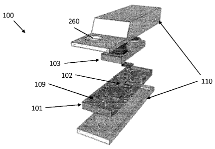
FIG. 26 illustrates a de-assembled device 100 according to embodiments of the
present invention, comprising a fluidic substrate 101 comprising an inlet 109
and a
microfluidic component 102, a lid 103 and an package 110. The package 110 may
comprise a base and a top which can be assembled together to package the
fluidic
substrate 101 and the lid 103, thus protecting these from environmental
influences such
as dust. The package may comprise a through-hole 260 for depositing a fluid
sample
on an inlet 109 of the fluidic substrate 101. When all parts are assembled,
the device
100 may function as a stand-alone wireless device for analyzing a fluid
sample.
According to embodiments of the present invention, at least a part of the lid
103
may be in contact with the fluid sample when the fluid sample is present in
the device
100. As the lid 103 is a CMOS chip, electronic circuitry present on a surface
of the chip
may be in direct contact with the fluid sample when the lid 103 is functioning
as a side-
wall of an open micro-fluidic component 102 in the fluidic substrate 101. In
this case,
the side of the chip comprising electronic circuitry may be bonded to an open
micro-
fluidic component 102 of the fluidic substrate 101 wherein the electronic
circuitry is
aligned with parts of the micro-fluidic component 102 where interaction with a
fluid
sample is desired. As an advantage, this may improve the interaction between
the
electronic circuitry and the fluid sample.
According to embodiments of the present invention, the lid 103 may comprise
bonding layers to enable bonding of the lid 103 to the fluidic substrate 101.
According to embodiments of the present invention, a first side of the fluidic
substrate 101 comprising an open micro-fluidic component 102 may be bonded to
a
first side of the CMOS chip 103 comprising at least one electrical component.
According to an embodiment, the lid 103 comprises a transistor layer, the
transistor layer being electrically connected at least one electrical
component, the
electrical component being at least one of the following: biosensing
circuitry, electrodes
CA 02912947 2015-11-19
WO 2014/187926 PCT/EP2014/060591
is
for sensing purposes, electrodes for fluid manipulation purposes, circuitry
for data
communication purposes, circuitry for wireless data communication purposes,
temperature sensors, heater electrodes for temperature control or temperature
cycling
and fluid sensors and electrodes for fluidic viscosity control. The circuitry
for wireless
data communication may comprise provisions for communication via a Bluetooth
radio
or a WiFi module for wirelessly transmitting data from electronic circuitry in
the lid 103.
As an advantage, the device 100 may communicate with an external device such
as a
mobile device which may be used to further process the data.
The lid 103 is a CMOS chip. According to embodiments of the present invention,
the CMOS chip comprises a silicon substrate 111, a transistor layer 112, at
least one
electrical component electrically connected to the transistor layer 112 and at
least one
bonding layer 115.The at least one electrical component may be biosensing
circuitry,
electrodes for sensing purposes, electrodes for fluid manipulation purposes,
circuitry
for data communication purposes, circuitry for wireless data communication
purposes,
temperature sensors, heater electrodes for temperature control and fluid
sensors and
electrodes for fluidic viscosity control.
A particular embodiment of a lid 103 according to embodiments of the present
invention is illustrated in FIG. 18. In this embodiment, the CMOS chip 103
comprises a
silicon substrate 111. Atop the silicon substrate 111 a transistor layer 112
may be
present. Atop the transistor layer 112 an interconnection layer 113 may be
present.
Atop the transistor layer 112, at least one electrical component may be
present
electrically connected to the transistor layer 112 via the interconnection
layer 113. The
interconnection layer 113 may comprise a plurality of metal layers. According
to
embodiments of the present invention, atop the transistor layer 112 , a
bonding layer
115 and at least one electrode 114 may be present. The electrode 114 may be
electrically connected to the transistor layer via the interconnection layer
113.
According to embodiments of the present invention, the at least one electrical
component may be a biocompatible electrode which is fluid corrosion free and
chemically inert. According to a specific embodiment, the at least one
electrode 114 is
TiN electrode.
According to embodiments of the present invention the bonding layer 115 may be
a layer which allows bonding of the CMOS chip 103 to the fluidic substrate 101
at low
temperatures and voltages. This is advantageous as these conditions do not
damage
the CMOS chip, neither do they damage reagents or for instance proteins which
may
CA 02912947 2015-11-19
WO 2014/187926 PCT/EP2014/060591
16
be provided on the microfluidic substrate 101. According to a specific
embodiment, the
bonding layer 115 may be a Si02 or polymer layer.
FIG. 19 illustrates a device 100 according to embodiments of the present
invention, wherein a CMOS chip 103 as illustrated in FIG. 18 is bonded to a
fluidic
substrate 101. The side of the CMOS chip 103 comprising the bonding layer 115
and
the electrode 114 is bonded to the side of the fluidic substrate 101
comprising an open
micro-fluidic component 102. This means that the CMOS chip 103 as illustrated
in
FIG. 18 is flipped upside down with respect to its position as illustrated in
FIG. 18. The
electrode 114 is thereby in direct contact with a fluid sample present in the
micro-fluidic
component 102. The bonding layer 115 is used to attach the CMOS chip 103 to
the
fluidic substrate 101.
According to embodiments of the present invention, the CMOS chip 103 may
comprise at least one silicon I/O connection 116, as illustrated in FIG. 20.
The silicon
I/O connection 116 may be a backside opening through the substrate 111 to
access
electrical signals of the CMOS chip 103 in the transistor layer 112. Further,
in yet
alternative embodiments, the silicon I/O connection 116 may be a backside
opening
through both the substrate 111 and the transistor layer 112 to access
electrical signals
of the CMOS chip 103 in the interconnection layer 113. FIG. 20 illustrates the
device
100 wherein a CMOS chip 103 is bonded to a fluidic substrate 101 and wherein
the
CMOS chip 103 features a silicon I/O connection 116 through both the substrate
111
and the transistor layer 112.
According to embodiments of the present invention, the fluidic substrate may
comprise an open micro-fluidic component 102 and the fluidic substrate may be
covered
partly by the CMOS chip 103. It is advantageous that a part of the micro-
fluidic
component 102 is not covered as this allows reagents to be applied/spotted on
specific
open parts of the micro-fluidic component 102. In this case, no extra through-
holes are
needed to apply reagents after bonding of the fluidic substrate 101 to the
CMOS chip
103. It is also advantageous that the CMOS chip area is smaller, as the active
electronics is the more expensive part of the disposable.
According to embodiments of the present invention, the CMOS chip 103 may
further comprise at least one I/O pad 117. The at least one I/O pad 117 may be
located
on the interconnection layer 113.
FIG. 21 illustrates an embodiment of a CMOS chip 103. The CMOS chip 103
comprises a silicon substrate 111. Atop the silicon substrate a transistor
layer 112 is
CA 02912947 2015-11-19
WO 2014/187926 PCT/EP2014/060591
17
present. Atop the transistor layer 112, an interconnection layer 113 is
present. The
interconnection layer 113 may comprise a plurality of metal layers to
interconnect the
transistor layer 112 with electrical components. Atop the transistor layer
112, a bonding
layer 115, an I/O pad 117 and, in the embodiment illustrated, a plurality of
electrodes
114 are present. The electrodes 114 are electrically connected to the
transistor layer
112 via the interconnection layer 113. The I/O pad 117 is also electrically
connected to
the transistor layer 112 via the interconnection layer 113.
According to embodiments of the present invention, a first part of a first
major
surface of the CMOS chip 103 may cover the fluidic substrate 101, a second
part of the
first major surface of the CMOS chip 103 may not cover the fluidic substrate
101. In
these embodiments, the CMOS chip 103 may either be larger than the fluidic
substrate
101, or it may be laterally shifted with respect to the fluidic substrate 101
so that a
portion of the CMOS chip 103 forms an overhang with respect to the fluidic
substrate
101. The second part of the first major surface of the CMOS chip 103 may
comprise at
least one I/O pad 117 to have access to the I/O pad 117.
FIG. 22 illustrates a CMOS chip 103 as illustrated in FIG. 21, bonded to a
fluidic
substrate 101. A first part of the CMOS chip 103 at least partly, and in the
embodiment
illustrated fully covers the fluidic substrate 101 wherein electrodes 114 are
in direct
contact with a fluid sample when present in the micro-fluidic component 102 of
the
device 100. The bonding layers 115 are used to bond a first part of the CMOS
chip 103
to the fluidic substrate 101. A second part of the CMOS chip 103 forms an
overhang
which does not cover the fluidic substrate 101. The second part comprises the
I/O pad
117. As an advantage, this overhang allows easy access to the I/O pad 117.
This allows
standard I/O pad dimensions and packaging approaches to be used for inserting
the
substrate in slots typically used for smartcards. It is a further advantage
that additional
processing steps to fabricate silicon I/O connections (e.g. a hole through the
substrate
and transistor layer) to access electrical signals in the CMOS chip 103 are
not required.
According to embodiments of the present invention, the fluidic substrate 101
further comprises at least one optical waveguide to allow optical excitation
and sensing
of the fluid sample when present in the device 100.
According to embodiments of the present invention, the fluidic substrate 101
or
the lid 103 comprises at least one through-hole for application of a
biochemical reagent
to a region of the micro-fluidic component 102 or to a region of the lid 103.
The through-
holes in the fluidic substrate 101 or the lid 103 allow the application of
biochemical
CA 02912947 2015-11-19
WO 2014/187926 PCT/EP2014/060591
18
reagents to specific regions of the micro-fluidic component 102 or to specific
regions of
the lid 103. This is advantageous as it allows reagents to be applied after
attachment
of the lid 103 to the fluidic substrate 101.
According to embodiments of the present invention, the CMOS chip 103 may
comprise at least one through-hole 118. When attached to the fluidic substrate
101, the
through hole 118 in the CMOS chip 103 allows reagent spotting on a specific
location
of the micro-fluidic component 102 in the fluidic substrate 101 or on a
specific part of
the CMOS chip 103. FIG. 23 illustrates such an embodiment wherein the CMOS
chip
103 comprises one through hole 118. In this embodiment, the CMOS chip further
comprises a silicon I/O connection 116. As illustrated, the CMOS chip 103
completely
covers a part of the fluidic substrate 101.
According to same or alternative embodiments of the present invention, a first
side of the fluidic substrate 101 comprises the open micro-fluidic component
102. The
other side, opposite to the side where the micro-fluidic component 102 is
provided, may
comprise a at least one through hole 119. The through hole 119 allows reagent
spotting
on a specific location of the micro-fluidic component 102 in the fluidic
substrate 101 or
on a specific part of the CMOS chip 103. FIG. 24 illustrates such an
embodiment
wherein the fluidic substrate comprises two through holes 119. A part of the
CMOS chip
103 covers the fluidic substrate 101, the part not covering the fluidic
substrate 101 but
forming an overhang comprises an I/O pad 117.
According to embodiments of the present invention, the lid 103 may be bonded
to the fluidic substrate 101 using a polymer, which may preferably be a
lithographically
patterned polymer. The material for forming the bonding between the lid 103
and the
fluidic substrate 101 should be suitable for perform a Si-Si bonding,
preferably at low
temperature, for instance room temperature. This is compatible with CMOS
circuits
being present on the lid 103 and which should not be destroyed by the bonding
process,
and with reagents being present on or in the fluidic substrate 101, and which
should
also not be destroyed by the bonding process. Suitable bonding materials for
bonding
the lid 103 to the fluidic substrate 101 are for instance photopatternable
PDMS,
obtainable from Dow Corning; 5U8, obtainable from Micr Chem; or OSTE,
obtainable
from Mercene Labs. These bonding materials all have room temperature as
bonding
temperature.
According to another embodiment of the present invention, the lid 103 is
bonded
to fluidic substrate 101 using a CMOS compatible packaging technique. The use
of
CA 02912947 2015-11-19
WO 2014/187926 PCT/EP2014/060591
19
CMOS packaging techniques may be used when the fluidic substrate 101 is a
silicon
substrate and the lid 103 is a CMOS chip.
According to embodiments of the present invention, the device 100 may further
comprise metal contacts electrically connected to the lid 103 for read-out of
electrical
signals from the lid 103. The metal contacts may be located on the lid 103,
electrically
connected to electronic circuitry in the lid 103. The position and shape of
the metal
contacts may be selected according to standards, allowing insertion of the
device in
standardized slots such as slots for memory cards (e.g. CompactFlash,
SmartMedia,
MultiMedia Card or Secure Digital (SD) memory cards) commonly used in
communication devices such as mobile devices. The insertion of the device 100
in an
mobile device allows processing of the electrical signals from the lid 103 by
a processor
and/or other electronic components present in the mobile device. For example,
a
processor of a smartphone may be used to process electrical signals and/or to
display
data.
According to embodiments of the present invention, at least a part of the
fluidic
substrate 101 and/or the lid 103 may be fabricated from a transparent material
to allow
optical inspection of a fluid sample when the fluid sample is present in the
micro-fluidic
component 102. The part of the fluidic substrate 101 that is fabricated from a
transparent material may be part of the micro-fluidic component 102 of the
device 100.
The transparent part may be a side-wall of the micro-fluidic component 102 of
the
device 100. The transparent material allows optical inspection of a fluid
sample in the
device 100. An optical detector may be used to optically inspect a fluid
sample, in order
for instance to detect an analyte. The optical detector may be an image sensor
which
may be part of an external device or may be integrated in the device 100. The
transparent material may be a transparent oxide or polymer. For microscopy
purposes,
a part of the lid 103 or a part of the fluidic substrate 101 may be
transparent. For lens-
free imaging purposes, a part of the lid 103 and a part of the fluidic
substrate 101 may
be transparent to enable working in transmission mode wherein a radiation
source may
be used to radiate an object in a fluid sample in the device 100 through the
transparent
part of the lid 103 and a detector may be used to detect signals from the
radiated object
through the transparent part of the fluidic substrate 101. The signals may be
diffraction
patterns of a radiated object in the fluid sample.
FIG. 33 illustrates a device 100 according to embodiments of the present
invention, where a fluidic substrate 101 and a lid 103 are bonded to one
another. The
CA 02912947 2015-11-19
WO 2014/187926 PCT/EP2014/060591
fluidic substrate 101 comprises different microfluidic components for multi-
omic
analysis, in the embodiment illustrated comprising a plurality of chambers
330, 331,
332, 333 and microfluidic channels (not illustrated). The chambers may have
different
depths, depending on their function and the type of measurement being
performed. The
5
chambers may be separated by valves that may be actuated in any suitable way,
for
instance by fluidic forces or by electricity. Electrodes for actuation may be
provided on
the fluidic substrate 101 or on the lid 103. The CMOS chip forming the lid 103
may thus
incorporate different functionalities, such as for instance a CMOS microscopic
imager
334, CMOS optical detectors 335, 336 and CMOS electrical circuitry 337 for
heating
10 and/or
sensing. The CMOS microscopic imager 334 may comprise CMOS active pixels
for readout of optical signals from the fluid sample in the microfluidic
component 102.
The CMOS optical detector 335 comprises an optical resonator 338. A waveguide
339
may be present for transporting measurement light from one location of the
CMOS chip
103 to another location. The waveguide may for instance be used for
irradiating the
15 sample
for performing lensfree microscopy. Furthermore, filters may be provided in
the
fluidic substrate 101 or in the lid 103 for rejecting optical excitation from
emission, so
as to enable measurement of a fluorescent signal. Also multispectral filters
may be
provided in the fluidic substrate 101 or in the lid, for measurement
fluorescent signals
with multiple colours.
20 This
way, detection of different types of markers can be performed within a single,
preferably disposable, detection device according to embodiments of the
present
invention.
According to embodiments of the present invention, the shape of the device 100
allows insertion into a mobile communication device. According to embodiments
of the
present invention, the device 100 has the shape/dimensions of a memory card.
It is an
advantage of embodiments of the present invention that the dimensions of the
device
100 may be according to standards, e.g. according to standards of memory cards
used
in mobile devices such as: CompactFlash, SmartMedia, MultiMedia Card, Secure
Digital memory cards or any other type.
FIG. 31 and 32 illustrate an embodiment of the present invention wherein the
device 100 has the shape of an SD card. Inside the cut-out 106 (which is
always present
according to SD card standards), a needle 104 is present. At the other side of
the SD
card, the metal contacts are present and electrically connected to the lid 103
to allow
CA 02912947 2015-11-19
WO 2014/187926 PCT/EP2014/060591
21
read-out of electrical signals from the lid 103 which may be further processed
by the
device in which the SD card is inserted.
According to embodiments of the present invention, the lid 103 or the fluidic
substrate 101 may further comprise a compartment for powering the device 100,
such
as a battery compartment (not illustrated) which is electrically connected to
the lid 103.
In a second aspect embodiments of the present invention relate to a method to
fabricate a device as disclosed in the first aspect of the present invention.
The method
comprises: providing a fluidic substrate 101; providing a lid 103; attaching
the fluidic
substrate 101 to the lid 103 to close the fluidic substrate 101 at least
partly;
characterized in that: the fluidic substrate 101 is a silicon fluidic
substrate and the lid
103 is CMOS chip; and wherein the fluidic substrate 101 is attached to the lid
103 using
a CMOS compatible bonding process.
It is advantageous that the fluidic substrate 101 is bonded to the lid 103
using a
CMOS compatible bonding process. In state of the art devices, bonding is
performed
using high temperature/voltage bonding techniques. These bonding techniques
may
damage electronic circuitry present in the CMOS chip and/or reagents present
in the
microfluidic substrate 101. The use of a CMOS compatible bonding enables
bonding at
lower temperatures/voltages and therefore preserves the electronic circuitry
of the lid
103 and the reagents present in the microfluidic substrate 101. According to
embodiments of the present invention, the bonding may be performed via a wafer
to
wafer or die to wafer bonding process such as direct oxide to oxide bonding or
bonding
via a pattern-able polymer. Additionally, it can also be advantageous to be
able to
perform the bonding at a low temperature in case some reagents are already
spotted
on one of the substrates during the fabrication flow.
The fluidic substrate 101 may be fabricated using a combination of coarse and
fine structures in a single piece of silicon substrate by a combination of two
hard masks,
protection and de-protection of layers, etching of coarse and etching of fine
structures.
The fine structures may be structures configured to enable a controlled
capillary suction
in the micro-fluidic component 102 of the device 100. The fine structures may
comprise
micro-pillars 270 and/or other microstructures. The coarse structures may be
structures
for storing larger volumes of fluids e.g. reagent storage 102b for storing
reagents, or a
wick 102i. It is an advantage to use silicon rather than more common
microfluidic
materials such as glass or polymers since the very high anisotropic etching of
silicon
results in fine structures with extremely high aspect ratios. The silicon
micro-pillars 270
CA 02912947 2015-11-19
WO 2014/187926 PCT/EP2014/060591
22
typically have lateral dimensions from 1 um to 20 um with aspect ratios of 20-
50. High
aspect ratios are advantageous in having a high surface to volume ratio,
essential for
capillary flow. The high aspect ratio fine structures, combined with the
coarse structures
allow to implement more complex capillary fluidic functions in a more compact
footprint
than is achievable with any other material. More complex functions include
separation
(e.g. cells from molecules), mixing, valving, thermally controlled
reactions,... Moreover,
silicon is an inert material with clear advantages towards implementation of
biochemical
reactions. The advantage of the extremely compact fully integrated disposable
device
results from the advanced use of silicon for both the fluidic substrate and
the CMOS lid.
The reduced footprint also results in reduced cost of the entire device.
According to embodiments of the present invention, providing a fluidic
substrate
101 comprises providing a silicon substrate 201, illustrated in FIG. 11, and
patterning
the silicon substrate to form a micro-fluidic component 102 and a means for
providing
a fluid sample in the device 100, the micro-fluidic component 102 being
configured to
propagate a fluid sample via capillary force through the device 100.
According to embodiments of the present invention, providing a fluidic
substrate
101 comprises: providing a silicon substrate 201, providing an oxide mask 202,
patterning the oxide mask 202 by using a first patternable mask layer 210, so
as to
create fine structures 203 in the oxide mask 202 (FIG. 12); providing a
protection layer
204 to protect the patterned oxide mask; patterning coarse structures in a
second
patternable mask layer 211 (FIG. 13); etching of the coarse structures 205 in
the silicon
substrate 201 through the second mask layer 211 (FIG. 14); removing the second
mask
layer 211 and growing oxide 206 (FIG. 15) for protecting the coarse structures
205;
removing the protection layer 204 (FIG. 16) and etching the fine structures
203 using
the oxide layer 206 as an etch mask (FIG. 16); removing the oxide 206 (FIG.
17). The
resulting structure is a microfluidic substrate 101 which may be used in a
device
according to embodiments of the first aspect of the present invention.
FIG. 11-17 illustrate how the fluidic substrate 101 may be fabricated.
According
to embodiments of the present invention, the fluidic substrate 101 may be
fabricated by
performing:
- Patterning fine structures 203 comprising: providing a silicon substrate
201,
providing an oxide mask 202, patterning the oxide mask 202 to create fine
structures 203 in the oxide mask 202;
- providing a protection layer 204 to protect the oxide 202;
CA 02912947 2015-11-19
WO 2014/187926 PCT/EP2014/060591
23
- performing lithography of coarse structures 205;
- performing etching of the coarse structures 205;
- growing oxide 206 for protecting the coarse structures 205 wherein the
protection layer 204 on the fine structures 203 prevents oxide growth;
- removing the protection layer 204 and etch the fine structures 203;
- removing the oxide 206.
According to embodiments of the present invention, the protection layer 204
may
be a nitride layer.
According to embodiments of the present invention, providing the CMOS chip 103
comprises: providing a silicon substrate 111, fabricating a transistor layer
112 atop the
silicon substrate and providing an interconnection layer 113 atop the
transistor layer.
The interconnection layer may comprise at least one metal layer. The CMOS chip
103
is fabricated using standard CMOS process techniques.
Further, on top of standard CMOS process flows, additional components may be
deposited or patterned on the interconnection layer 113 such as biocompatible
electrodes, a bonding layer, I/O pads or other components.
According to embodiments of the present invention, through holes 109, 118 may
be etched through the fluidic substrate 101 or the CMOS chip 103 to enable
fluidic
access for applying of reagents to the fluidic substrate 101 or CMOS chip 103.
The
through-holes in the CMOS chip 103 may be fabricated whilst fabricating
silicon I/O
interconnections 116 in the CMOS chip 103. The through-holes in the fluidic
substrate
101 may be fabricated by first thinning the fluidic substrate 101 and then
etching the
through-holes.
According to embodiments of the present invention, the CMOS chip 103 may be
bonded to the fluidic substrate 101 using a die to wafer or wafer to wafer
bonding
process.
To access electrical signals of the CMOS chip 103, silicon I/O contacts 116
may
be provided. According to embodiments of the present invention, the contacts
may be
fabricated by thinning the silicon substrate 111 of the CMOS chip 103 and
performing
a back side etching on the silicon substrate 111 to gain access to a metal
layer of the
interconnection layer 113.
Alternatively, a CMOS chip 103 comprising an I/O pad 117 at a first side of
the
chip 103 may be provided, wherein the first side of the CMOS chip 103 is
bonded to the
fluidic substrate 101 and wherein the first side of the CMOS chip 103
comprising the
CA 02912947 2015-11-19
WO 2014/187926 PCT/EP2014/060591
24
I/O pad 117 does not cover the fluidic substrate 101. This is for example
illustrated in
FIG. 22. The I/O pad 117 is accessible when the CMOS chip 103 is bonded to the
fluidic
substrate 101. The I/O pad 117 may be used as a metal contact on a memory
card.
According to embodiments of the present invention, the CMOS chip 103 is
bonded to the fluidic substrate 101 while aligning at least one electrical
component on
a first side of a CMOS chip 103 with the micro-fluidic component 102. For
example,
sensing and actuating electrodes on the first side of the CMOS chip 103 are
aligned
with a sensing or actuation side in the fluidic substrate 101. This allows
direct contact
of a fluid sample with electrical components present on the CMOS chip 103 when
a
fluid sample is present in the device 100.
According to embodiments of the present invention, surfaces of the fluidic
substrate 101 and the lid 103 are partially or fully coated to modify surface
interactions
with the fluid sample. The surfaces may be inner surfaces of the micro-fluidic
component 102 or a surface of the CMOS chip 103 that is bonded to the fluidic
substrate
101. In particular those parts of the surface of the CMOS chip 103 that are in
contact
with a fluid sample present in the micro-fluidic component 102. The coating
may be a
hydrophilic coating.
The surfaces of the micro-fluidic component 102 and/or the side of the CMOS
chip 103 bonded to the fluidic substrate 101 can be made hydrophilic in order
to improve
the wetting behavior of the surfaces, thereby promoting capillary flow. The
surfaces can
also be treated in order to avoid absorption or adhesion of biomolecules on
the walls.
The coating can be done for example by vapor coating with silanes. According
to
embodiments of the present invention the coating may be performed locally on
certain
parts of the fluidic substrate 101 (e.g. in some micro-fluidic channels) or on
certain parts
of the CMOS chip 103.
According to embodiments of the present invention, at least one through-hole
is
fabricated in the fluidic substrate 101 by first etching the through-hole and
then filling
the through-holes with a transparent oxide of polymer.
Embodiments of the present invention improve the functionality, portability
and
manufacturability of compact disposable point of care devices. A particular
embodiment
of the present invention is a fully integrated silicon device with a needle or
an inlet for
the intake of blood or any other body fluid. The device features a capillary
fluidic system
for the propagation of a fluid sample through the device via capillary action.
A capillary
pump functioning as the wicking zone of the capillary fluidic system may be
used to
CA 02912947 2015-11-19
WO 2014/187926 PCT/EP2014/060591
propagate the fluid sample in the device. A sensor chip reading out signals
produced
by biochemical sensing reactions inside the capillary system may be used to
add
biosensing functionality to the device. Further, the device features a data
communication interface for sending data to a personal computer, a computing
unit,
5 smartphone or any other wireless communication device. The device may
function as
a stand-alone system wherein a power interface such as a battery powers
electronic
circuitry such as a micro-chip in the device. Alternatively, the device may be
powered
via a communication port of the device.
The device may further comprise fluidic manipulation structures including
filtering,
10 mixing, valves structures. A protection structure with a cut off zone to
protect and
prevent breaking the needle before usage may be present to avoiding
contamination
before usage. Structures such as electrically controllable fluidic
manipulation structures
including electrowetting, electro and dielectrophoretic manipulation may be
present to
interact with a fluid sample in the device. Electronic controllable heaters
may be present
15 for accurately controlling the temperature of the chip or for thermal
cycling purposes.
Another exemplary embodiment of the present invention includes an elegant, low
cost and compact manner to fabricate all of the above functions by providing a
silicon
substrate which may comprise lithographically defined channels, micro pillars
and
microstructures of various shapes fabricated by deep Reactive Ion Etching and
20 designed to function as a capillary fluidic platform. The silicon
substrate may have a
provision for making a needle and a cut off zone for protecting the needle.
The silicon
substrate can have different etch depths allowing for precise control over the
volume
and capillary flow of a fluid sample in the device. The silicon substrate may
be closed
by a CMOS substrate (= lid 103) comprising CMOS electronics containing a
transistor
25 layer. The electronics may be designed to provide functionality
including sensing,
actuating, signaling, data processing and data communication and therefore
replaces
the point of care instrument. Some of the electrodes may be in direct contact
with the
fluid, these electrode may be protected in a fluid compatible manner. The
silicon
substrate may be closed by the CMOS substrate by bonding both substrates in a
leakage free and biocompatible manner. This can be done via a wafer to wafer
or die
to wafer bonding process such as bonding via a patternable polymer. The inner
silicon
substrate surfaces which may be in contact with the body fluids may feature a
hydrophilic layer via coating of the inner channels. Additionally, through
wafer holes
may be fabricated in the silicon substrate for supplying reagents after the
device has
CA 02912947 2015-11-19
WO 2014/187926 PCT/EP2014/060591
26
been bonded. For each analysis, different reagents can be supplied. As an
advantage,
the same device becomes configurable for different diseases by simply adding
reagents
through the through-holes in the last production step. The device may be
manufactured
using CMOS compatible processing steps which lower production cost and enable
the
device to be used as disposable device.
Further, the device may comprise components to enable interfacing with
standard
user interfaces. For example, the use of such a device as a smartcard in
wireless
communication devices inserted in slots typically foreseen for smartcards. For
example,
the use of such a device together with a compact and cheap battery and low
cost
communication device (e.g. Bluetooth, NFC). For example, the use of such a
device
together with a wired communication interface (e.g. USB)
Embodiments of the present invention may be used to detect DNA/RNA from
body fluids and perform an analysis to detect: mutations (ancestry, drug
dosing, disease
predisposition), miRNA (marker for cancer and other diseases), pathogen
DNA/RNA
(infectious diseases such as HepC, HIV, etc.), microbiome DNA. Further, the
device
may be used to detect proteins such as biomarkers for a specific disease
(cancer,
Alzheimer's, infectious diseases, heart disease, cancer etc.) Further, the
device may
be used to detect small molecules and metabolites to reveal metabolic
information
(cholesterol). Further, the device may be used to detect biomarkers from
exosomes.
Further the device may be used to perform microscopy to perform a blood count,
analyze cells present in the blood (e.g. circulating tumour cells), identify
infectious
agents (e.g. malaria) and to detect blood disorders (e.g. sickle cell anemia).