Note: Descriptions are shown in the official language in which they were submitted.
CA 02912955 2015-11-19
WO 2014/190801
PCT/CN2014/074438
METHOD OF MARKING MATERIAL AND SYSTEM THEREFORE, AND
MATERIAL MARKED ACCORDING TO SAME METHOD
FIELD OF THE INVENTION
The present invention relates to a method of providing a marking on a solid
state
material. In particular, the present invention relates to providing a marking
on a
surface of a solid state material such as a gemstone or the like, whereby the
marking is not optically viewable.
BACKGROUND OF THE INVENTION
Marking of solid materials, in particular precious gemstones or the like, may
be
required for example in identification or quality markings. For the marking of
gemstones, it is desirable that marking be performed in a manner such that the
gemstone is not damaged or any damage is minimised, the integrity of the
gemstone is preserved, no significant loss in mass occurs, no chemical residue
remains, and the marking does not detract from the clarity or colour of the
gemstone.
For ornamental gemstones, the marking technique should not be visible to the
naked eye so as not to detract from the quality of the stone from an aesthetic
standpoint, whereby visible identification of marking may detract from the
visual
result in devaluation of a gemstone.
The techniques of etching, engraving and micro-milling processes exist in the
prior
art, which may impact on the integrity and quality of a gemstone, and may be
1
CA 02912955 2015-11-19
WO 2014/190801
PCT/CN2014/074438
viewed unfavourably. Furthermore, such processes result in some amount of loss
of material, again which may be viewed unfavourably.
Other marking techniques exist within the prior art including those such as
disclosed in US Patent US6,391,21561, whereby an information mark is applied
to a polished facet of a diamond or silicon carbide gemstone whereby the
gemstone is coated with an electrically conductive layer. The electrically
conductive layer prevents the gemstone from becoming charged and the mark is
formed by a focused ion beam whereby a portion of the surface is ablated to a
requisite depth, and whereby the surface to which the mark is applied is
subsequently cleaned utilising a powerful oxidizing agent.
OBJECT OF THE INVENTION
Accordingly, it is an object of the present invention to provide a method of
providing a marking on a solid state material and a solid state material
having said
marking thereon, which overcomes or at least partly ameliorates at least some
of
the deficiencies as associated with the prior art.
SUMMARY OF THE INVENTION
In a first aspect, the present invention provides a method of forming one or
more
protrusions on an outer surface of a polished facet of a solid state material,
said
method including the step of:
(i) applying focused inert gas ion beam local irradiation towards an outer
surface of a polished facet of a solid state material in a way of protruding
top
surface material;
2
CA 02912955 2015-11-19
WO 2014/190801
PCT/CN2014/074438
wherein irradiated focused inert gas ions from said focused inert gas ion
beam penetrate the outer surface of said polished facet of said solid state
material;
and
wherein irradiated focused inert gas ions cause expansive strain within the
solid state crystal lattice of the solid state material below said outer
surface at a
pressure so as to induce expansion of solid state crystal lattice, and form a
protrusion on the outer surface of the polished facet of said solid state
material.
Preferably, the focused inert gas ion beam has a beam energy in the range of
from 5keV to 50keV and probe current in the range of 1fA to 200pA.
The solid state crystal lattice may be in the form of a single crystalline,
poly-
crystalline, or amorphous form, and the solid state material is a material in
solid
state form under ambient temperature and under a pressure from atmospheric to
high vacuum.
Preferably the solid state material is a precious stone. More preferably, the
solid
state material is a material selected from the group including Diamond, Ruby,
Sapphire, Emerald, Pearl, Jade or the like.
The focused inert gas ion beam is an ion source which may be selected from any
inert gas in Group VIII of the periodic table.
Preferably, the polished facet of the solid state material has an average
surface
roughness of less than 50nm.
3
CA 02912955 2015-11-19
WO 2014/190801
PCT/CN2014/074438
Preferably, the protrusion has an average width in the nanometer or micrometer
order of magnitude, and an average height in the nanometer or micrometer order
of magnitude.
The distance from the outer surface of said solid state material to the region
of
irradiated inert gas accumulation below the outer surface is preferably in the
range
of from mm to 100pm.
The protrusion may be provided so as to form an identifiable mark or pattern,
and
the identifiable mark is in the form of a single or array of dot, pillar,
dome,
hemisphere, line, irregular shape, symmetric or asymmetric shape, or the like.
The identifiable mark may be provided as a periodic line array, hole/dot
array,
circular array, spiral array, fractal array or multiple periods array, or the
like.
Alternatively, the identifiable mark may be provided as a continuous protruded
shape to form arbitrary patterns.
A plurality of protrusions may be formed that are nanometer sized so as to
provide
an information mark invisible to the naked eye due to Rayleigh Criterion in
optical
limit. The protrusions may be arranged in a periodic array viewable by
specified
lighting conditions and by a camera equipped microscope in the visible and
invisible light range. The one or more protrusions forms an identifiable
security
mark.
The method preferably maintains integrity of said solid state material such
that
there exists substantially no loss in mass.
4
CA 02912955 2015-11-19
WO 2014/190801
PCT/CN2014/074438
In a second aspect, the present invention provides a solid state material
having
one or more protrusions formed on an outer surface of a polished facet of the
solid
state material, wherein said one or more protrusions are formed from a method
including the step of:
(i) applying focused inert gas ion beam local irradiation towards an outer
surface of a polished facet of a solid state material in a way of protruding
top
surface material;
wherein irradiated focused inert gas ions from said focused inert gas ion
beam penetrate the outer surface of said polished facet of said solid state
material;
and
wherein irradiated focused inert gas ions cause expansive strain within the
solid state crystal lattice of the solid state material below said outer
surface at a
pressure so as to induce expansion of solid state crystal lattice, and form a
protrusion on the outer surface of the polished facet of said solid state
material.
Preferably, the focused inert gas ion beam has a beam energy in the range of
from 5keV to 50keV and probe current in the range of lfA to 200pA.
The solid state crystal lattice may be in a form of single crystalline, poly-
crystalline,
or amorphous form. The solid state material is a material in solid state form
under
ambient temperature and under a pressure from atmospheric to high vacuum.
The solid state material is preferably a precious stone, and more preferably
selected from the group including Diamond, Ruby, Sapphire, Emerald, Pearl,
Jade
or the like.
5
CA 02912955 2015-11-19
WO 2014/190801
PCT/CN2014/074438
The focused inert gas ion beam utilised to form said one or more protrusions
is an
ion source which may be selected from any inert gas in Group VIII of the
periodic
table.
Preferably, the polished facet of the solid state material has an average
surface
roughness of less than 50nm.
The protrusion preferably has an average width in the nanometer or micrometer
order of magnitude, and an average height in the nanometer or micrometer order
of magnitude.
Preferably, the distance from the outer surface of said solid state material
to the
region of irradiated inert gas accumulation below the outer surface is in the
range
of from mm to 100pm.
The one or more protrusions are preferably provided so as to form an
identifiable
mark or pattern. The identifiable mark may be in a form of single or array of
dot,
pillar, dome, hemisphere, line, irregular shape, symmetric or asymmetric
shape, or
the like.
Alternatively, the identifiable mark may be provided as a periodic line array,
hole/dot array, circular array, spiral array, fractal array or multiple
periods array, or
the like, or the identifiable mark may be provided as a continuous protruded
shape
to form arbitrary patterns.
The solid state material may have a plurality of protrusions formed which are
nanometer sized so as to provide an information mark invisible to the naked
eye
due to Rayleigh Criterion in optical limit. The protrusions may be arranged in
a
6
CA 02912955 2015-11-19
WO 2014/190801
PCT/CN2014/074438
periodic array viewable by specified lighting conditions and by a camera
equipped
microscope in the visible and invisible light range.
The one or more protrusions may form an identifiable security mark.
The integrity of solid state material is preserved such that during formation
of the
one or more protrusions, there exists substantially no loss in mass of the
solid
state material.
In a third aspect, the present invention provides a system for forming one or
more
protrusions on an outer surface of a polished facet of a solid state material,
said
system including:
a focused inert gas ion beam device for applying focused inert gas ion
beam local irradiation towards an outer surface of a polished facet of a solid
state
material
a computer control device for controlling discharge of a focused inert gas
ion beam local irradiation towards an outer surface of a polished facet of a
solid
state material,
wherein the computer control device controls irradiated focused inert gas
ions from said focused inert gas ion beam so as to penetrate the outer surface
of
said polished facet of said solid state material; and irradiated focused inert
gas
ions cause expansive strain within the solid state crystal lattice of the
solid state
material below said outer surface at a pressure so as to induce expansion of
solid
state crystal lattice, and so as to form a protrusion on the outer surface of
the
polished facet of said solid state material.
7
CA 02912955 2015-11-19
WO 2014/190801
PCT/CN2014/074438
Preferably, the focused inert gas ion beam device has a beam energy in the
range
of from 5keV to 50keV and probe current in the range of 1fA to 200pA.
The focused inert gas ion beam utilised to form said one or more protrusions
is an
ion source which may be selected from any inert gas in Group VIII of the
periodic
table.
The system provides a protrusion having an average width in the nanometer or
micrometer order of magnitude, and an average height in the nanometer or
micrometer order of magnitude.
Preferably, the system is adapted to provide a protrusion whereby the distance
from the outer surface of said solid state material to the region of
irradiated inert
gas accumulation below the outer surface is in the range of from lnm to 100pm.
The system is adapted so as to provide an identifiable mark or pattern on an
outer
surface of a polished facet of a solid state material. The identifiable mark
provided
by the system may be in a form of a single or array of dot, pillar, dome,
hemisphere, line, irregular shape, symmetric or asymmetric shape, or the like.
Alternatively, the identifiable mark may be provided as a periodic line array,
hole/dot array, circular array, spiral array, fractal array or multiple
periods array, or
the like. The identifiable mark may be provided as a continuous protruded
shape
to form arbitrary patterns.
Preferably, the system is adapted to provide a plurality of protrusions which
are
nanometer sized so as to provide an information mark invisible to the naked
eye
due to Rayleigh Criterion in optical limit.
8
CA 02912955 2015-11-19
WO 2014/190801
PCT/CN2014/074438
The system is preferably adapted so as to provide a plurality of protrusions
which
are arranged in a periodic array viewable by specified lighting conditions and
by a
camera equipped microscope in the visible and invisible light range.
The system may be adapted to provide one or more protrusions so as to form an
identifiable security mark.
The system is adapted so as to maintain the integrity of said solid state
material
during formation of the one or more protrusions, and such that there exists
substantially no loss in mass of the solid state material.
Preferably, the system is adapted so as to provide one or more protrusions on
the
outer surface of a precious stone. More preferably, the system is adapted so
as to
provide one or more protrusions on the outer surface of a Diamond, Ruby,
Sapphire, Emerald, Pearl, Jade or the like.
The system is preferably adapted so as to provide one or more protrusions on a
polished facet of the solid state material having an average surface roughness
of
less than 50nm.
The system is preferably adapted so as to provide one or more protrusions on
the
outer surface of a solid state material, wherein the one or more protrusions
has an
average width in the nanometer or micrometer order of magnitude, and an
average height in the nanometer or micrometer order of magnitude.
Preferably, the system is adapted so as to provide one or more protrusions on
the
outer surface of a solid state material such that the region of irradiated
inert gas
accumulation below the outer surface is in the range of from lnm to 100pm.
9
CA 02912955 2015-11-19
WO 2014/190801
PCT/CN2014/074438
BRIEF DESCRIPTION OF THE DRAWINGS
Preferred embodiments of the present invention will be explained in further
detail
below by way of examples and with reference to the accompanying drawings, in
which:-
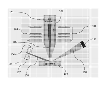
Figure 1 shows an exemplary schematic diagram of a configuration of a focused
inert gas ion beam system as utilised in embodiments of the present invention;
Figure 2 shows an exemplary schematic representation of a computer stimulated
interaction volume of incident energetic focused inert gas ions with a solid
state
material specimen at a top surface region, in accordance with embodiments of
the
present invention;
Figure 3 shows an exemplary schematic representation depicting interaction of
primary incident energetic inert gas ion with a solid state specimen, the
Figure
showing the production of charged particles such as electrons and ions along
the
displaced path of incident ion, in accordance with embodiments of the present
invention;
Figure 4 depicts an ion microscope image of an experimentally protruded array
of
nanometer sized dots, in accordance with embodiments of the present invention;
Figure 5 depicts an ion microscope image of a further experimentally protruded
array of nanometer sized dots, in accordance with embodiments of the present
invention;
CA 02912955 2015-11-19
WO 2014/190801
PCT/CN2014/074438
Figure 6 depicts an ion microscope image of another experimentally protruded
array of nanometer sized dots, in accordance with embodiments of the present
invention;
Figure 7a depicts a graph showing a schematic representation of a surface
profile
of an untreated flat surface;
Figure 7b depicts a graph of a schematic representation of the profile of
protruded
surface according to embodiments of the present invention;
Figure 8 depicts a schematic three-dimensional contour representation of a
protruded surface profile on a flat surface with proportional dimensions in
reference to the experimental results as described with reference to Figures
4, 5
and 6;
Figure 9a depicts an ion microscope image of an untreated surface on a single
crustal diamond facet with a programmed dot array to be incident by focused
inert
gas ion beam in accordance with embodiments of the present invention; and
Figure 9b depicts an ion microscope image of the surface of the single crystal
diamond facet of Figure 9a, after incident by focused inert bas ion beam at
assigned position on the diamond specimen surface, in accordance with
embodiments of the present invention.
DETAILED DESCRIPTION OF THE PREFERRED EMBODIMENTS
Referring to Figure 1, there is shown an exemplary schematic diagram of a
configuration of a focused inert gas ion beam system 100 as utilised in
accordance with embodiments of the marking method of the present invention.
11
CA 02912955 2015-11-19
WO 2014/190801
PCT/CN2014/074438
In comparison to typical scanning electron microscopy (SEM), the focused inert
gas ion beam system 100 has a similar basic configuration, whereby the
schematic diagram of Figure 1 shows the configuration of a focused inert gas
ion
beam system 100 for producing and imaging the protruded array of nanometer
sized dots in accordance with embodiments of the present invention is shown.
The gas sources 101 at the top of the electrostatic lens column 102 may be any
known inert gases in Group VIII of the periodic table, and the choice of inert
gas
sources utilised depends on the requisite resulting resolution and fabrication
time.
Further, an inert gas is preferably utilised in order to minimise any
alterations in
electrical, optical, or chemical properties of a specimen to be marked.
For example, for the fabrication of protruded nanometer sized dots is shown
and
discussed further below in reference to Figure 4, Figure 5 and Figure 6, a low
pressure of the inert gas with light atomic mass is preferred, such as Helium
or
Neon gas for the gas source 101 of the focused inert gas ion beam system 100.
Once the inert gas ion is emitted from the gas source 101, it is accelerated
and
focused along the top of the electrostatic lens column 102, and then deflected
by
scanning deflectors 103 and 104 which are controlled by a computer system,
typically a mainframe computer control system or the like, which finally forms
a
scanning focused inert gas ion beam 105 to incident on surface of a specimen
109.
During the scanning or continuous incident of the focused inert gas ion beam
105
to incident on surface of the specimen 109, a beam 108 of electrons or
negative
charges emitted from an emission device 106 and 107, such as electron flood
gun
12
CA 02912955 2015-11-19
WO 2014/190801
PCT/CN2014/074438
or charge compensator, is used to compensate the positively charged up
specimen surface 109 due to continuous incident of gas ions on specimen
surface
109.
As the charged up ions inhibit further incident of focused inert gas ions 105,
this
results in image burr or drift in position or shape of a requisite protruded
mark.
During incident of the focused inert gas ion beam 105 on the surface of the
specimen 109, the interaction of incident inert gas ions with the surface of
the
specimen 109 produces different charged species 110 such as electrons or ions
which are detected by an ion or electron detector 111 for imaging, species
qualification and quantification.
Referring to Figure 2, there is shown an exemplary schematic representation of
a
computer simulated interaction volume of incident energetic focused inert gas
ions
with a solid state material specimen 203 at a top surface region, 202 in
accordance with the present invention, whereby an example of the computer
simulated Monte Carlo plot is depicted showing of the trajectory of the
incident
ions 204 during the interaction of an incident energetic focused inert gas ion
beam
201 with a top surface region 202 of a solid state material specimen 203.
The Monte Carlo simulation of the interaction is based upon Helium ion as the
source of incident energetic focused inert gas ion beam 201 which is
accelerated
at 30keV and the solid state material specimen 203 is silicon substrate.
The cross-section of interaction volume of the solid state material specimen
203 is
defined with the penetration depth 205 and dispersed width 206 which is
perpendicular to penetration depth 205 of incident ions, and the Monte Carlo
13
CA 02912955 2015-11-19
WO 2014/190801
PCT/CN2014/074438
simulated numerical results of the penetration depth 205 and dispersed width
206
is about 100nm.
Further, due to a high penetration depth and less lateral straggle of Helium
gas
ion into the silicon substrate, the size of the focused ion beam spot 207 at
the top
surface region 202, in range of 10nm, is as small as lnm or less in order to
fulfill
the requisite criteria of embodiments of the present invention in creating
requisite
nanometer sized structures or marks.
Referring to Figure 3, the detailed interaction of incident energetic inert
gas ion
301 with a solid state material 305 as utilised in accordance with embodiments
of
the present invention is schematically shown.
For explanatory purposes of embodiments of the present invention, the
experimental environment is assumed to be in high vacuum, such as at pressure
of 5x10⁻⁶ Torr or lower pressure, and the energetic inert gas ion 301 incident
along
the path 302 is at an incident angle 303 to the surface or interface 304
between
vacuum and the solid state specimen 305.
At the instance of energetic inert gas ion 301 incident at the specimen
surface or
interface 304, possible energetic species 306 may be generated such as
secondary electrons, Auger electrons, X-ray, secondary ions, sputtered
particles
from the solid state specimen 305, or even back-scattered energetic inert gas
ion
301.
The circumstance of said possible energetic species depends on the atomic mass
and carried energy of energetic inert gas ion 301, density and crystallinity
of the
14
CA 02912955 2015-11-19
WO 2014/190801
PCT/CN2014/074438
solid state specimen 305, chemical bonding between atoms, and the charge state
of the specimen surface or interface 304.
If the energetic inert gas ion 301 has sufficient energy, then there exists a
high
probability of entry of said energetic species into the solid state specimen
305 and
continued to penetration.
Along the propagation paths 309 and 312, the energetic inert gas ion 301 may
possibly undergo inelastic collision with adjacent atoms inside the solid
state
specimen 305, and one possibility is the generation of energetic species 311
such
as secondary ion or secondary electron and possibly coming along the path 310
out from the specimen surface or interface 304.
Another possibility is for said possible energetic species to stop at certain
local
regions for example 308 and 313 as depicted inside the solid sate specimen 305
due to energy loss as resulting in accumulation of inert gas ion or
amorphisation
of crystalline at local regions 308 and 313.
By appropriate control of the condition of the incident angle 303 of the
energetic
inert gas ion 301, accelerating voltage, and species selection of energetic
inert
gas ion 301, the incident energetic inert gas ion 301 has high probability to
stop at
region 308 and result in either or both accumulation of inert gas ion or
amorphisation of crystalline at local region which has lower density but
larger
volume than crystalline structure.
Thus, local internal strain is built up within the solid state specimen 305
slightly
below the specimen surface or interface 304 which finally leads to expansion
of
solid state crystalloid lattice at the specimen surface or interface 304,
hence
CA 02912955 2015-11-19
WO 2014/190801
PCT/CN2014/074438
resulting in the formation of a protruded dot 307 in accordance with
embodiments
of the present invention.
Referring to the ion microscope image as depicted in Figure 4, there is shown
an
experimentally protruded array of nanometer sized dots 401 on single crystal
diamond facet 402 by the focused inert gas ion beam system.
The acceleration voltage of gas ions utilised is about 35kV, and the beam
current
utilised is about 0.5pA with ions dose of about 0.1nC/pm2, and the dwell time
is of
about lus. As will be understood, other applicable acceleration voltages and
beam currents may be utilised, whilst falling within the scope of the present
invention. For example, a focused inert gas ion beam device utilising focused
inert
gas ion beam having a beam energy in the range of from 5keV to 50keV and
probe current in the range of 1fA to 200pA, will be understood to be
applicable,
although utilizing equipment capable of generating parameters outside of 5keV
to
50keV and probe current in the range of 1fA to 200pA, may also be considered
by
those skilled in the art to be applicable to embodiments of the present
invention.
The incident position of the focused inert gas ion beam is programmed by the
computer and then controlled by scanning lens column 103 and 104 as
exemplified and described with to Figure 1, and as results as shown in Figure
4,
the array of 3 x 3 protruded nanometer sized dots is formed with each
protruded
nanometer sized dots 401 having diameter of about 130nm and the vertical
period
403 and horizontal period 405 with reference to the plane of the diamond facet
402, displacement between centers of adjacent protruded nanometer sized dots
401, are same of about 200nm.
16
CA 02912955 2015-11-19
WO 2014/190801
PCT/CN2014/074438
The field of view of whole image in this example as shown in both vertical and
horizontal directions is 2.00pm x 2.00pm under magnification of 57,150 X,
which
in this example is imaged by the same focused inert gas ion beam system after
fabrication of protruded nanometer sized dots 401, and with the same
acceleration
voltage of gas ions but less beam current than under scanning mode.
The scale bar 404 is shown for reference to the dimension of the protruded
nanometer sized dots 401.
Similarly to Figure 4, Figure 5 shows an exemplary embodiment of a protruded
array of nanometer sized dots 501 fabricated by the focused inert gas ion beam
system on single crystal diamond facet 502, however the diameter of the
protruded nanometer sized dots 501 in this example is reduced to 80nm and both
the vertical period 503, and the horizontal period 505 is increased to 400nm.
The reduction of the protruded nanometer sized dots 501 diameter is achieved
by
reducing the inert gas ions dose to less than 0.05nC/pm2 and also reducing the
beam current to less than 0.5pA.
The imaging conditions of Figure 5 are the same as set in Figure 4 with the
scale
bar 505 for reference.
By way of a further exemplary embodiment, further reducing the inert gas ions
dose, for example to 0.03nC/pm2 or less, and also further reducing the beam
current to 0.4pA or less, the diameter of the protruded nanometer sized dots
601
is reduced to 50nm fabricated on single crystal diamond facet 602 as shown in
Figure 6.
17
CA 02912955 2015-11-19
WO 2014/190801
PCT/CN2014/074438
The array of protruded nanometer sized dots 601 has both the same vertical
period 603 and horizontal period 605 as shown in Figure 5 with a similar scale
bar
604 for reference and comparative purposes.
As will be understood and appreciated by those skilled in the art, the
exemplary
embodiments as described with reference to Figure 4, Figure 5, and Figure 6
show that the diameter of protruded nanometer sized dots can be controlled by
appropriately tuning the incident gas ions dose and the probe current, hence
the
beam size of incident gas ions, from diameter of 200nm shown in Figure 4, to a
significantly lower size down to 50nm shown in Figure 6.
Furthermore, the change of the both vertical and horizontal periods in the
protruded array of nanometer sized dots from 200nm as shown in Figure 4 to
400nm as shown in both Figure 5, and Figure 6, indicate that the focused inert
gas ion beam has the ability and efficacy to be utilised to fabricate those
protruded
nanometer sized dots at arbitrary positions on a specimen surface as a result
of a
protruded mark in a form of a single or array of dot, pillar, dome,
hemisphere, line,
irregular shape, symmetric or asymmetric shape, or arbitrary shape which is in
periodic line array, hole/dot array, circular array, spiral array, fractal
array or
multiple periods array, by way of example.
Reference is made to Figures 7a and 7b, in order to further explain the
geometry
of the protruded nanometer sized dots, whereby a schematic graph shows the
cross-sections between the surface profiles of untreated flat specimen surface
702 and the protruded surface 703 with nanometer sized dots.
18
CA 02912955 2015-11-19
WO 2014/190801
PCT/CN2014/074438
With reference to the Z-direction axis 701, the untreated flat surface 702 of
Figure
7a is at the level of Z=0 whilst the protruded surface 703 of Figure 7b is
deformed
to the positive sign of Z-direction, thus having a profile higher than the
untreated
flat surface 702.
Further space upper than the untreated flat surface 702 or the protruded
surface
703 may be exposed to air/vacuum in the positive sign of Z-direction axis,
whilst in
the negative side of Z-direction the specimen depth may be finite or semi-
infinite.
The height 705 of the protruded surface 703 is defined as being from the
displacement of the protruded surface 703 top from Z=0 while the width or
diameter 704 of the protruded surface 703 or dot is defined as the greatest
displacement between two lowest points in the surface profile of the protruded
surface 703 just above Z=0.
Referring to Figure 8, there is shown an example of schematic three-
dimensional
contour diagram of a protruded mark 801 profile so as to provide for enhanced
illustration, appreciation and understanding of the shape of the protruded
mark
801 fabricated on flat surface 802 by focused inert gas ion beam.
The height of the protruded mark, has the same definition as 705 explained and
discussed in reference to Figure 7b, whereby the protruded mark 801 extends
from the flat surface 802 in reference to axis 803, while the width and depth
have
the same definition as 704 as explained and described in reference to Figure
7a
and Figure 7b, of the protruded mark 801 are in reference to 804 and 805
respectively.
19
CA 02912955 2015-11-19
WO 2014/190801
PCT/CN2014/074438
In reference to the illustrative example of Figure 8 to those protruded
nanometer
sized dots shown in Figure 4, Figure 5 and Figure 6, the dimension units of
all
axes 803, 804 and 805 are in nanometers.
Referring to the ion microscope images shown in Figure 9a and Figure 9b, an
exemplary embodiment of the invention is shown whereby the feasibility is
demonstrated of fabricating a predetermined and designed nanometer sized
continuous pattern or mark 905 on single crystal diamond facet 902 and 906 by
a
programmed array 903, whereby the energetic inert gas ion incident at which is
shown as white dots 901. The displacement between centers of adjacent white
dots 901 is about 120nm with reference to the scale bar 904.
By controlling the dose and beam current of the incident energetic inert gas
ions,
in order to achieve each protruded nanometer sized dot having a diameter of
not
less than 120nm, a continued protruded line 905 and further a two-dimensional
protruded pattern or mark 907 on facet 906 with a size of around 800nm x
800nm,
with reference to the scale bar 908, instead of discrete dots has been formed
as
shown in Figure 9b.
Those skilled in the art will appreciate that the present invention allows for
the
provision of numerous other and alternate embodiments utilising the
methodology
and process of the present invention, so as to provide marking to a solid
state
material in a predetermined manner, for a variety of applications depending
upon
the requirements of such applications.
The present invention provides a method and system for the application of a
marking to a solid state material and a marked solid state material resulting
CA 02912955 2015-11-19
WO 2014/190801
PCT/CN2014/074438
therefrom, preferably a precious stone, which provides marking having the
advantages including those of the following:
(i) marking which is not unsightly and which may not be readily viewed
without the knowledge of specific parameters for the viewing and
identification of such marking;
(ii) marking, which when applied to precious stones or gemstones, allows
for
identification for security purposes, as well as tracking and origin
purchases, benefits and advantages in the precious stone industry;
(iii) security purposes for marking of solid state materials which may be
identified in the event of impropriety, theft or the like;
(iv) marking of a solid state material, without the disadvantages
associated
with destructive and invasive methods of marking such as etching,
ablation, millings, engravings or the like;
(v) a methodology and product thereof which does not result in removal of
material or any significant loss in weight or mass of the solid state
material to which the marking is to be applied;
(vi) a methodology and product thereof which does not alter the optical
properties of a solid state material, and which does not detrimentally
affect the clarity or colour of the solid state material;
(vii) a methodology and product thereof which utilises an inert gas, and
does
not introduce contaminants or impurities to the solid state material;
21
CA 02912955 2015-11-19
WO 2014/190801
PCT/CN2014/074438
(viii) a methodology and product thereof which obviates the necessity of
post-
processing of the solid state material;
(ix) a methodology and product thereof that requires no significant removal
of
material from the surface of solid state material;
(x) a methodology and product thereof which obviates the necessity of pre-
treatment of coating of the solid state material prior to application of
marking;
(xi) a methodology and product thereof, having no associated chemical
residue;
(xii) a methodology and product thereof which obviates the necessity of
post-
processing and the utilisation of complex post-processing techniques
such as chemical and plasma cleaning and the like.
By providing a method of marking a surface of solid state material by applying
focused inert gas ion beam local irradiation in a way of protruding up a top
surface
of a material to form patterns or marks, due to expansion of solid state
crystalloid
lattice underneath its top surface by the force of inert gas accumulation or
amorphisation of crystalline underneath, instead of etching, engraving,
milling or
removing top surface material, which are concerned as destructive and invasive
and ablative to the solid state material, the present invention provides
significant
advantages over those of the prior art.
Those skilled in the art will appreciate the advantages associated with such a
marking technique and methodology for solid state material which may be
utilised
22
CA 02912955 2015-11-19
WO 2014/190801
PCT/CN2014/074438
and implemented in other applications in addition to those as described in the
exemplary embodiments and examples thereof.
While the present invention has been explained by reference to the examples or
preferred embodiments described above, it will be appreciated that those are
examples to assist understanding of the present invention and are not meant to
be
restrictive. Variations or modifications which are obvious or trivial to
persons
skilled in the art, as well as improvements made thereon, should be considered
as
equivalents of this invention.
23