Note: Descriptions are shown in the official language in which they were submitted.
CA 02913575 2015-12-01
DISTRIBUTED CONTROL OF A MODULAR SWITCHING SYSTEM
CROSS-REFERENCE TO RELATED APPLICATIONS
The present application claims the benefit of United States Patent Application
14/953,442
filed on November 30, 2015.
FIELD OF THE INVENTION
The invention is related to a modular switching system configured as a large-
scale data
center or a network of global coverage. In particular, the invention is
concerned with distribution
of control data in a modular switching system having a large number of
switches.
SUMMARY
In accordance with one aspect, the present invention provides a switching
system
comprising switches interconnecting edge nodes. The switches are logically
arranged in a matrix
of a number of columns and the same number of rows. Each switch has a number
of input ports
and the same number of output ports and is coupled to a respective switch
controller.
Each edge node is communicatively coupled to an input port of each switch of a
respective row and an output port of each switch of a respective column. To
facilitate
distribution of control data from the switches to the edge nodes, each switch
and its diagonal
mirror, forming a diagonal pair, with respect to the matrix are spatially
collocated. Switch
controllers of a first switch and a second switch of each diagonal pair of
switches are
communicatively coupled.
With the matrix of switches of p, columns and rows, u>2, a diagonal pair of
switches
comprises a switch of column j and row k and a switch of column k and row j,
j#1c, the columns
being indexed as 0 to (u--I) and the rows being indexed as 0 to ( -1).
In addition to the input ports and output ports connecting to edge nodes, the
switching
mechanism of a switch may provide a control inlet and a control outlet. The
switch controller of
a switch may be coupled to the control inlet and control outlet so that an
edge node may
communicate with the switch controller through an input port, the switching
mechanism, and the
1
CA 02913575 2015-12-01
outlet port and, conversely, the switch controller may communicate with an
edge node through
the control inlet, the switching mechanism, and an output port.
Other means of communication between edge nodes coupled to a switch and a
controller
of the switch may be devised; for example by providing separate control paths
from each input
port of a switch to a controller of the switch and separate paths from the
controller of the switch
to output ports of the switch. Thus edge nodes connecting to the input ports
may send upstream
control data to the switch controller and the switch controller may send
downstream control data
to edge nodes connecting to the output ports of the switch.
A switch controller of a switch comprises a scheduler for scheduling data
transfer
through the switch and a timing circuit for exchanging timing data with each
edge node
connecting to the switch. A master time indicator is coupled to the switch
controllers of the two
switches of a diagonal pair of switches.
According to an embodiment, the edge nodes of the switching system may be
communicatively coupled to the switches through intermediate spectral routers.
With this
method of coupling, the input ports of a switch connect to output channels of
a spectral
demultiplexer and the output ports of the switch connect to input channels of
a spectral
multiplexer. The spectral demultiplexer directs individual spectral bands from
an upstream
wavelength-division-multiplexed link originating from all edge node to
respective input ports of
the switch. The spectral multiplexer combines spectral bands from the output
ports of the switch
onto a downstream wavelength-division-multiplexed link terminating at an edge
node.
Thus, the switching system employs a plurality of upstream spectral routers
and a
plurality of downstream spectral routers. Each spectral router connects a set
of upstream
wavelength-division-multiplexed (WDM) links originating from a respective set
of edge nodes to
a set of WDM links each terminating on a single switch. Each downstream
spectral router
connects a set of WDM links each originating from a single switch to a
respective set of
downstream WDM links each terminating on a single edge node.
According to another embodiment, the edge nodes of the switching system may be
communicatively coupled to the switches directly. With this method of
coupling, the switches
2
CA 02913575 2015-12-01
would be organized into constellations of switches where the switches of each
constellation are
spatially collocated. Each constellation may be organized in the form of a sub-
matrix of A rows
and A columns of switches, A>1. With the matrix of switches having columns and
IA rows, is
selected as an integer multiple of A.
A constellation of switches is coupled to A arrays of spectral demultiplexers
and A arrays
of spectral multiplexers. Each spectral demultiplexer directs spectral bands
of a respective
upstream WDM link to an input port of each switch of a row of the
constellation. Each spectral
multiplexer combining spectral bands from an output port of each switch of a
column of the
constellation onto a respective downstream WDM link. Each edge node is
communicatively
coupled to the switches through an upstream WDM link to each constellation of
a respective row
of constellations and a downstream WDM link from each constellation of a
respective column of
constellations. An upstream WDM link connects an edge node to input of a
spectral
demultiplexer coupled to a constellation. A downstream WDM link connects
output of a spectral
multiplexer coupled to a constellation to an edge node.
In accordance with another aspect, the present invention provides a method of
switching
data among a plurality of edge nodes. The method comprises arranging a
plurality of switches in
a matrix of )1 columns and p. rows, >2, collocating the two switches of each
diagonal pair of
switches, mutually coupling controllers of the two switches of a diagonal pair
of switches, each
switch being coupled to a respective controller, and coupling the two switches
of a diagonal pair
of switches to a respective master time indicator.
Control data is communicated from a first controller of a first switch of a
diagonal switch
pair to a first edge node connected to an input port of the first switch along
a first control path
traversing a second controller of a second switch of the diagonal switch pair
and a switching
mechanism of the second switch.
Control data is communicated from the second controller to a second edge node
connected to an input port of the second switch along a second control path
traversing the first
controller and a switching mechanism of the first switch.
3
CA 02913575 2015-12-01
The method further comprises performing, at the respective controller of a
particular
switch, processes of scheduling data transfer through a switching mechanism of
the particular
switch and exchanging timing data with each edge node connecting to the
particular switch.
The method further comprises receiving at the first controller timing data
from the first
edge node and correlating at the first controller the received timing data
with a reading of the
master time indicator. A result of the correlation is communicated to the
first edge node through
the first control path.
The method further comprises receiving at the second controller additional
timing data
from the second edge node and correlating at the second controller the
received additional timing
data with a reading of the master time indicator. A result of the correlation
is communicated to
the second edge node through the second control path.
The method further comprises adding (2>< 1) new switches as a new column of
switches
and a new row of switches to the matrix of switches and providing m additional
edge nodes, m
being a number of input ports and a number of output ports of each switch of
the plurality of
switches. Each edge node of the additional edge nodes connects to an input
port of each switch
of (11+1) switches of the new row of switches. The m input ports of each
switch of remaining IA
switches connect to a set of edge nodes connecting to one of the rows of
switches.
The method further comprises indexing edge nodes of the plurality of edge
nodes
sequentially where edge nodes connecting to a row of index q and a column of
index q,
are indexed as (j+mxq), Oij<m, thereby the index of an edge node remains
unchanged as the
switching system grows to accommodate more edge nodes.
The method further comprises adding an input port and an output port to each
switch of
the plurality of switches and providing additional edge nodes. Each edge node
of the additional
edge nodes connects to an input port of each switch of a row of index q and an
output port of
each switch of a column of index q, 19q<1_1.
The method further comprises indexing edge nodes of the plurality of edge
nodes
sequentially where edge nodes connecting to a row of index q and a column of
index q,
4
CA 02913575 2015-12-01
are indexed as (q+p.xj), Oi<m. Thus, the index of an edge node remains
unchanged as the
switching system grows to accommodate more edge nodes.
in accordance with a further aspect, the present invention provides a
switching system
comprising a plurality of switches logically organized into a matrix of
constellations of
collocated switches. Each constellation comprises A rows and A columns of
switches, A>1. Each
switch coupled to a respective switch controller and comprises a number of
input ports and the
same number of output ports. Each constellation of switches is coupled to A
arrays of spectral
demultiplexers and A arrays of spectral multiplexers. A spectral demultiplexer
directs spectral
bands of a respective upstream WDM link to an input port of each switch of a
row of a
constellation. A spectral multiplexer combines spectral bands from an output
port of each switch
of a column of a constellation onto a respective downstream WDM link.
To interconnect edge nodes of a plurality of edge nodes, each edge node
connects to
constellations of a respective row and constellations of a respective column
of the matrix of
constellations. An edge node has a number of upstream WDM links, each directed
to a spectral
demultiplexer coupled to one of the constellations of the respective row, and
a number of
downstream WDM links each originating from a spectral multiplexer coupled to
one of the
constellations of the respective column.
Thus, each edge node connects to a respective set of spectral demultiplexers
coupled to
constellations of a row of matrix of constellations and respective set of
multiplexers coupled to
constellations of a column of matrix of constellations. The respective set of
spectral
demultiplexers and respective set of multiplexers are selected so that each
switch of a first
constellation and a corresponding switch of a second constellation constitute
a complementary
switch pair, where said first constellation and said second constellation
constitute a diagonal
constellation pair.
BRIEF DESCRIPTION OF THE DRAWINGS
Features and implementations will be further described with reference to the
accompanying exemplary drawings, in which:
5
CA 02913575 2015-12-01
FIG. 1 illustrates switches logically arranged in a matrix of switches for use
in illustrating
switching-system growth according to a first growth scheme;
FIG. 2 illustrates a plurality of edge nodes interconnected through switches
of the matrix
of switches of FIG. 1;
FIG. 3 illustrates a switch of the matrix of switches of FIG. 1;
FIG. 4 illustrates connectivity of a set of source nodes connecting to
switches of a sub-
matrix of the matrix of switches of FIG. 1;
FIG. 5 illustrates connectivity of a set of sink nodes connecting to switches
of the sub-
matrix of FIG. 4 according to the first growth scheme, where each sink node is
integrated with a
respective source node to form an edge node;
FIG. 6 illustrates connectivity of another set of source nodes connecting to
switches of
the sub-matrix of FIG. 4;
FIG. 7 illustrates connectivity of another set of sink nodes connecting to
switches of the
sub-matrix of FIG. 4;
FIG. 8 and FIG. 9 illustrate an increased number of edge nodes (source nodes
and sink
nodes) connecting to switches of another sub-matrix of the matrix of switches
of FIG.
according to the first growth scheme;
FIG. 10 and FIG. 11 illustrate further growth of the number of edge nodes
(source nodes
and sink nodes) connecting to the switches of the matrix of switches of FIG. I
according to the
first growth scheme;
FIG. 12 illustrates switches logically arranged in a matrix of switches for
use in
illustrating switching-system growth according to a second growth scheme;
FIG. 13 and FIG. 14 illustrate edge nodes (source nodes and sink nodes)
connecting to
the switches of FIG. 12 for use in illustrating the second growth scheme;
FIG. 15 and FIG. 16 illustrate a larger number of edge nodes (source nodes and
sink
nodes) connecting to the switches of FIG. 12 according to the second growth
scheme;
6
CA 02913575 2015-12-01
FIG. 17 and FIG. 18 illustrate further growth of the number of edge nodes
(source nodes
and sink nodes) connecting to the switches of FIG. 12 according to the second
growth scheme;
FIG. 19 illustrates diagonal switches along a diagonal of the matrix of
switches of FIG. 1;
FIG. 20 illustrates coupling of controllers of any complementary switch pairs,
in
accordance with an embodiment of the present invention;
FIG. 21, FIG. 22, FIG. 23, and FIG. 24 illustrate switch pairs each connecting
to a
respective dual controller where, for each switch pair, source nodes of a
respective first set of
edge nodes and sink nodes of a respective second set of edge nodes connect to
one of the
switches while source nodes of the respective second set of edge nodes and
sink nodes of the
respective first set of edge nodes connect to the other switch, in accordance
with an embodiment
of the present invention;
FIG. 25 illustrates source nodes connecting to rotators arranged in a matrix
of rotators, in
accordance with an embodiment of the present invention;
FIG. 26 illustrates connections of the rotators of FIG. 25 to sink nodes;
FIG. 27 illustrates a rotator coupled to a timing circuit;
FIG. 28 illustrates diagonal rotators each of which connecting to a respective
set of edge
nodes, where each edge node combines a source node and a sink node;
FIG. 29 illustrates coupling of timing circuits to rotators of any
complementary rotator
pair, in accordance with an embodiment of the present invention;
FIG. 30 and FIG. 31 illustrate rotator pairs each connecting to a respective
dual timing
circuit where, for each rotator pair, source nodes of a respective first set
of edge nodes and sink
nodes of a respective second set of edge nodes connect to one of the rotators
while source nodes
of the respective second set of edge nodes and sink nodes of the respective
first set of edge nodes
connect to the other rotator of the each rotator pair, in accordance with an
embodiment of the
present invention;
FIG. 32 illustrates connection of source nodes to switches through upstream
spectral
routers;
7
CA 02913575 2015-12-01
FIG. 33 illustrates connection of switches to sink nodes, through downstream
spectral
routers;
FIG. 34 illustrates direct connection, through upstream WDM links, of source
nodes to a
number of constellations of switches, in accordance with an embodiment of the
present
invention;
FIG. 35 illustrates connection of constellations of switches to sink nodes
through
downstream WDM links, in accordance with an embodiment of the present
invention;
Each of FIG. 36, FIG. 37, and FIG. 38 illustrate upstream connections from
edge nodes to
switches through an assembly of upstream spectral routers;
FIG. 39, FIG. 40, and FIG. 41 illustrates downstream connections from switches
to edge
nodes through an assembly of downstream spectral routers;
FIG. 42 illustrates a constellation of collocated switches indicating
collocated spectral
demultiplexers, each spectral demultiplexer separating spectral bands from a
WDM link
originating from a respective edge node;
FIG. 43 illustrates collocated spectral multiplexers coupled to the
constellation of
collocated switches of FIG. 42, each spectral multiplexer combining spectral
bands onto a WDM
link directed to a respective edge node;
FIG. 44 and FIG. 45 illustrate upstream connections of edge nodes to
constellations of
switches to eliminate the need for intermediate upstream spectral routers;
FIG. 46 and FIG. 47 illustrate downstream connections of edge nodes to
constellations of
switches to eliminate the need for intermediate downstream spectral routers;
FIG. 48 and FIG. 49 illustrate connecting edge nodes (source nodes and sink
nodes) to
constellations of switches of a network of global coverage, in accordance with
an embodiment of
the present invention; and
FIG. 50 illustrates a switching system based on the matrix of switches of FIG.
1 where
the two switches of each diagonal pair of switches are integrated to share a
common switching
mechanism, in accordance with an embodiment of the present invention.
8
CA 02913575 2015-12-01
TERMINOLOGY
Terms used in the present application are defined below.
Edge node (access node): A switching device connecting to data sources and
data sinks, and
configured to transfer data from the data sources to another switching device
and transfer data
from another switching device to the data sinks is referenced as an edge node
or access node.
Switch: A switch comprises a switching mechanism for transferring data from a
set of input ports
to a set of output ports. In the switching system of the present application,
a switch transfer data
from one set of edge nodes (access nodes) connecting to input ports of the
switch to another set,
or the same set, of edge nodes connecting to output ports of the switch. A
switch may use an
electronic or a photonic switching mechanism.
Collocation: The term refers to spatial proximity of devices which may be
interconnected using
relatively short links, such as fiber links each carrying a single spectral
band.
Dimension of a switch: The number of input ports and output ports, excluding
ports used
exclusively for control purposes, defines a "dimension" of a switch.
Global network: A network comprising a large number of nodes covering a wide
geographical
area is traditionally referenced as a global network.
Switching-system coverage: In a switching system configured as a network
comprising
geographically distributed access nodes (edge nodes), the term "coverage"
refers to the number
of access nodes.
Spectral multiplexer: A spectral multiplexer combines spectral bands of
separate input channels
onto an output wavelength-division-multiplexed link (WDM link), the input
channels which
originate from different switches.
Spectral demultiplexer: A spectral demultiplexer directs individual spectral
bands of an input
WDM link to separate output channels which may terminate onto different
switches.
Diagonal pair of switches: In a switching system employing a plurality of
switches logically
arranged in a matrix of switches having a number of columns and a same number
of rows, a
diagonal pair of switches comprises a switch of column j and row k and a
switch of column k
and row j, j#k, the columns being indexed as 0 to ( -1) and the rows being
indexed as 0 to ( -1),
9
CA 02913575 2015-12-01
ji being the number of columns. A switch of a column and a row of the same
index is referenced
as a "diagonal switch".
Complementary pair of switches: In a switching system employing a plurality of
switches
interconnecting a number of edge nodes, a complementary pair of switches
comprises a first
switch, transferring data from a first set of edge nodes to a second set of
edge nodes, and a
second switch transferring data from the second set of edge nodes to the first
set of edge nodes.
The complementary pair of switches may share a common controller or a dual
controller
comprising a first controller coupled to the first switch and a second
controller coupled to the
second switch where the two controllers are communicatively coupled to enable
transferring
control data from the first controller to the first set of edge nodes and
control data from the
second controller to the second set of edge nodes. Herein, the two switches,
and respective
controller(s), of a complementary pair of switches are considered to be
collocated.
Constellation of switches: A number of collocated switches form a
constellation.
Diagonal constellation pair: In a switching system employing a plurality of
switches arranged
into a matrix of constellations of collated switches having a number of x
columns and x rows,
x>1, a diagonal pair of constellations comprises a constellation of column j
and row k and a
constellation of column k and row j, j#k, the columns being indexed as 0 to (x-
1) and the rows
being indexed as 0 to (x¨l).
Diagonal pair of rotators: In a switching system employing a plurality of
rotators logically
arranged in a matrix rotators having a number of columns and a same number of
rows, a diagonal
pair of rotators comprises a rotator of column j and row k and a rotator of
column k and row j,
j#1:, the columns being indexed as 0 to ( -1) and the rows being indexed as 0
to ( -1), p. being
the number of columns. A rotator of a column and a row of the same index is
referenced as a
"diagonal rotator".
Complementary pair of rotators: In a switching system employing a plurality of
rotators
interconnecting a number of edge nodes, a complementary pair of rotators
comprises a first
rotator, transferring data from a first set of edge nodes to a second set of
edge nodes, and a
second rotator transferring data from the second set of edge nodes to the
first set of edge nodes.
CA 02913575 2015-12-01
Processor: The term "processor" as used in the specification of the present
application, refers to a
hardware processor, or an assembly of hardware processors, having at least one
memory device.
Controller: The term "controller", as used in the specification of the present
application, is a
hardware entity comprising at least one processor and at least one memory
device storing
software instructions. Any controller type, such as a "node controller",
"switch controller",
"domain controller", "network controller", or "central controller" is a
hardware entity.
Node controller: Each node, whether an ordinary node or a principal node, has
a node controller
for scheduling and establishing paths from input ports to output ports of the
node.
Software instructions: The term refers to processor-executable instructions
which may be applied
to cause a processor to perform specific functions.
Configuring a controller: The term refers to an action of installing
appropriate software for a
specific function.
Cross connector: The term is used herein to refer to a device having multiple
input ports and
multiple output ports where each input port cyclically 'connects to each
output port during a
repetitive time frame.
Channel: A directional channel is a communication path from a transmitter to a
receiver. A dual
channel between a first port having a transmitter and a receiver and a second
port having a
transmitter and a receiver comprises a directional channel from the
transmitter of the first port to
the receiver of the second port and a directional channel from the transmitter
of the second port
to the receiver of the first port. A channel may occupy a spectral band in a
wavelength division
multiplexed (WDM) link.
Link: A link is a transmission medium from a first node to a second node. A
link contains at
least one channel, each channel connecting a port of the first node to a port
of the second node. A
directional link may contain directional channels from ports of the first node
to ports of the
second node, or vice versa. A dual link comprises two directional links of
opposite directions.
WDM link: A number of channels occupying different spectral bands of an
electromagnetic
transmission medium form a wavelength-division-multiplexed link (a WDM link).
Spectral router: A spectral router (also called "wavelength router") is a
passive device
11
CA 02913575 2015-12-01
connecting a number of input WDM links to a number of output WDM links where
each output
WDM link carries a spectral band from each input WDM link.
Processor-executable instructions causing respective processors to route data
through the
switching system may be stored in a processor-readable media such as floppy
disks, hard disks,
optical disks, Flash ROMS, non-volatile ROM, and RAM. A variety of processors,
such as
microprocessors, digital signal processors, and gate arrays, may be employed.
A reference numeral may individually or collectively refer to items of a same
type. A
reference numeral may further be indexed to distinguish individual items of a
same type.
DETAILED DESCRIPTION
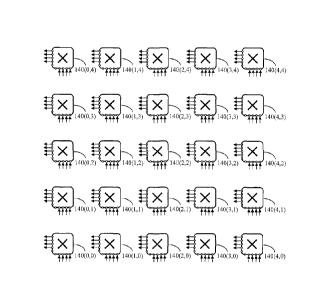
FIG. 1 illustrates switches 140 logically arranged in a matrix of switches
having
columns and u rows, u>2. The switches are individually identified as 140(j,k),
(Xj<u, (Xlc<pt,
where] and k are indices of a column and a row, respectively, of the matrix of
switches. In the
exemplary arrangement of FIG. 1, =5. Each switch 140 connects to respective
input channels
112 and respective output channels 114.
FIG. 2 illustrates edge nodes 220 which may be interconnected through the
matrix of
switches of FIG. 1. Each edge node 220 comprises a source node 224 and a sink
node 228. Each
edge node 220 (source node 224) connects to an upstream channel 230 to each
switch 140 of a
selected set switches. Each edge node 220 (sink node 228) connects to a
downstream channel
240 from each switch 140 of another selected set selected switches. A source
node 224 (edge
node 220) receives data from data sources through a number of channels 212. A
sink node 228
(edge node 220) transmits data from data sinks through a number of channels
214. Each edge
node 220 comprises a respective edge-node controller (not illustrated)
configured to
communicate with controllers of switching nodes or other switching-system
components. The
edge controller is a hardware entity which employs at least one hardware
processor, memory
devices storing software instructions, and memory devices storing control data
such as routing-
related data.
12
CA 02913575 2015-12-01
FIG. 3 illustrates a switch 140 comprising a number m of input ports 310, a
control inlet
312, a number m of output ports 330, and a control outlet 332. The m input
ports are individually
identified as input ports 310(0), 310(1), ..., 310(m-1), m>2. Them output
ports are individually
identified as output ports 330(0), 330(1), ..., 330(m-1). A switching
mechanism 320 selectively
transfers data from the input ports and the control inlet to the output ports
and the control outlet.
A switch controller 350 receives control data from the input ports 310 through
the switching
mechanism and control outlet 332. The switch controller 350 transmits control
data to the output
ports 310 through control inlet 312 and the switching mechanism. A master time
indicator 360
provides reference time to the switch controller. The switch controller 350 is
a hardware entity
comprising at least one hardware processor and a storage medium holding
software instructions
which cause the at least one hardware processor to implement routing and time
alignment
functions.
Growth of the Switching System
With the matrix of switches containing 1-12 switches 140 arranged into ji
columns and 11
rows, each switch having m dual ports (m input ports and m output ports), in
addition to control
inlets and outlets, the maximum number of edge nodes 220 supported by the
switching system
would be limited to 1.txm. To increase the number of edge nodes 220, the
dimension of each
switch, i.e., number rn of dual ports, may be increased, the number of
switches may be increased,
or both the dimension of each switch and the number of switches may be
increased,
In a first growth scheme, illustrated in FIG. 4 to FIG. 11, the dimension of
each switch is
kept unchanged and growth is realized by adding a column and a row of switches
140. Thus,
with a current switching system employing 112 switches, (2x1.1+1) switches are
added to increase
the number of edge nodes from laxm to (.txm+m). Each edge node 220 would then
have (1+1)
channels 218 to switches of a row of the matrix of switches and (j1+1)
channels 216 from
switches of a column of the matrix of switches. The edge nodes may be indexed
sequentially so
that edge nodes connecting to a row of index q and a column of index q, 0-
_q<i_t, are indexed as
(j+mxq),0<m. Thus, the index of an edge node remains unchanged as the
switching system
grows to accommodate more edge nodes.
13
CA 02913575 2015-12-01
In a second growth scheme, illustrated in FIG. 13 to FIG. 18, each edge node
220 has a
fixed number 1-1. of channels 218 to switches of a row of the matrix of
switches and the same
number t of channels 216 from switches of a column of the matrix of switches.
Thus, with the
number 1_1,2 of switches is unchanged. Growth is realized by adding a dual
port (an input port and
an output port) in each switch to increase the number of edge nodes from uxm
to (uxm+u). The
edge nodes may be indexed sequentially so that edge nodes connecting to a row
of index q and a
column of index q, 0:q<f_1, are indexed as (q+uxj), N<m. Thus, the index of an
edge node
remains unchanged as the switching system grows to accommodate more edge
nodes.
First Scheme of Switching-System Growth
FIG. 4 illustrates a selected set of source nodes 224 (edge nodes 220)
connecting to
switches of a sub-matrix 420 of the matrix of switches of FIG. I. The
exemplary arrangement of
switches of FIG. 1 comprises 25 switches arranged in five columns and five
rows. A switching
system may initially use switches of a sub-matrix of three columns and three
rows ( =3). Each =
source node 220 has an upstream channel 230 to each switch 140 of a row.
FIG. 5 illustrates a selected set of sink nodes 228 (edge nodes 220)
connecting to the
switches of FIG. 4, where each sink node 228 has a downstream channel 240 from
each switch
140 of a respective column. The connectivity patterns of FIG. 4 and FIG. 5 are
similar to the
connectivity pattern of FIG. 5 of U.S. Patent 7,760,716. Each sink node may be
integrated with a
respective source node to form an edge node.
According to the connectivity patterns of FIG. 4 and FIG. 5, an edge node 220
(224/228)
has an upstream channel 230 to a switch 140(j, k), and a downstream channel
240 from a switch
140(k, j), 0.<j<u, (X1(<1.1.
FIG. 6 illustrates another selected set of source nodes 224 connecting to
switches 140 of
sub-matrix 420 of switches of the matrix of FIG. 1.
FIG. 7 illustrates another selected set of sink nodes 228 connecting to the
switches of FIG.
4, where each sink node 228 has a downstream channel 240 from each switch 140
of a respective
column.
14
CA 02913575 2015-12-01
FIG. 8 and FIG. 9 illustrate growth of the switching system of FIG. 4 and FIG.
5,
according to a first growth scheme, using switches of a sub-matrix 820 of four
columns and four
rows ( =4). FIG. 8 illustrates source nodes 224 connecting to switches of a
sub-matrix 820. FIG.
9 illustrates sink nodes 228 connecting to witches 140 of sub-matrix 820 of
FIG. 8.
FIG. 10 and FIG. 11 illustrate further growth of the switching system of FIG.
8 and FIG.
9, according to the first growth scheme, to a switching system using all
switches of the matrix of
switches of FIG. 1 arranged in five columns and five rows ( =5).
FIG. 4, FIG. 6, FIG. 8, and FIG. 10 illustrate upstream connectivity of source
nodes to
respective switches. FIG. 5, FIG. 7, FIG. 9, and FIG. 11 illustrate downstream
connectivity of
switches to respective sink nodes.
Second Scheme of Switching-System Growth
FIG. 12 illustrates switches 1240 arranged in a matrix of switches of
according to a
second growth scheme where the dimension of each switch 140 of the matrix 100
of switches
may be increased to increase the coverage and capacity of the switching
system. The number of
supported edge nodes is uxm, and the access capacity of the switching system
is ax1i2xmxR,
where a, 0ot<1.0, is a design parameter and R is the capacity of each access
channel; R=2-
Gigabits/second, for example.
A switch 1240 is structurally similar to a switch 140. In the switching-system
configurations of FIG. 4 to FIG. 11, the number m of dual ports 310/330 is
kept unchanged
(m=4) while the number l of dual channels (upstream channels and downstream
channels)
connecting each edge node 220 to switches 140 is increased to grow the
switching system
according to the first growth scheme. In the switching-system configurations
of FIG. 13 to FIG.
14, the number j..t of dual channels connecting each edge node 220 to switches
1240 is kept
unchanged (1=3) while the number m of dual ports 310/330 is increased to grow
the switching
system according to the second growth scheme.
The switches 1240 of FIG. 12 are logically arranged in a matrix of switches
having 1.1
columns and 1j. rows, ).1>2. The switches are individually identified as
1240(j,k),
where j and k are indices of a column and a row, respectively, of the matrix
of switches. In the
CA 02913575 2015-12-01
exemplary arrangement of FIG. 12, =3. Each switch 1240 connects to respective
input channels
1212 and respective output channels 1214. Each switch 1240 of the exemplary
switch
arrangement comprises five input ports, five output ports, one control inlet,
and one control
outlet.
FIG. 13 and FIG. 14 illustrate source nodes 224 (edge nodes 220) connecting to
the
switches 1240 of FIG. 12 and sink nodes 228 (source nodes 220) connecting to
the switches of
FIG. 12, where each switch 1240 connects to three source nodes 224 and three
sink nodes 228
(m=3).
FIG. 15 and FIG. 16 illustrate growth of the switching system of FIG. 13 and
FIG. 14,
according to a second growth scheme, where each switch connects to four source
nodes and four
sink nodes (m=4). FIG. 15 illustrates source nodes 224 connecting to the
switches 1240 of FIG.
12 and FIG. 16 illustrates sink nodes 228 connecting to the switches 1240 of
FIG. 12.
FIG. 17 and FIG. 18 illustrate further growth of the switching system of FIG.
15 and FIG.
16, according to the second growth scheme, where each switch 1240 connects to
five source
nodes and five sink nodes (m=5). FIG. 17 illustrates source nodes 224
connecting to the switches
1240 of FIG. 12 and FIG. 18 illustrates sink nodes 228 connecting to the
switches 1240 of FIG.
12.
As defined earlier, a switch of column j and row j, 0_.j< , in a matrix of
switches having
columns and rows, p.>2, is referenced as a diagonal switch, the columns
being indexed as 0
to ( -1) and the rows being indexed as 0 to ( -1). A diagonal pair of switches
comprises a
switch of column j and row k and a switch of column k and row j, j#k of the
matrix of switches.
Routing control of the switching system
FIG. 19 illustrates diagonal switches 140(j, j), 0_j< , along a diagonal of
the matrix of
switches of FIG. I. Each edge node 220 which connects to an input port of a
switch 140(j,k),
where j=k, also connects to an output port of the same switch. Thus, where an
edge node 220
connects to a switch 140(j,j), there is a return control path from the edge
node 220 to itself, i.e.,
from the source node 224 to the sink node 228 of the same edge node, through
the same switch
140(j,j). This is not the case where k#j. In the configurations of FIG. 4 to
FIG. 11, each source
16
CA 02913575 2015-12-01
node 224 has a path to each sink node 228 through one of the switches 140.
Thus, when a source
node 224 and a sink node 228 of a same edge node 220 connect to different
switches, a return
control path from an edge node to itself can be provided through any
intermediate edge node 220.
However, it is preferable that such a return control path be created without
the need to traverse
an intermediate edge node 220. This can be realized by collocating a switch
140(j, k) with a
switch 140(k,j), where j#1(,0j< ,0j<1.t. A switch 140(j,k) and a switch
140(k,j), j#k, form a
"diagonal switch pair". With the connectivity schemes of FIG. 4 to FIG. 11,
switch 140(j,k) and
140(k,j) are also complementary switches forming a "complementary switch
pair".
FIG. 20 illustrates coupling of controllers of any complementary switch pairs
of the
matrix of switches 140 of FIG. 1 or the matrix of switches 1240 of FIG. 12 to
form a "dual
controller". A controller 2050(0), which comprises a scheduler and a timing
circuit for time-
aligning data arriving at inputs of a switching mechanism 320A of a switch
140(j, k), is coupled
through a dual channel 2055 to a similar controller 2050(1) of a switching
mechanism 320B of a
switch 140(k,j), j#k. The mutually coupled controllers 2050(0) and 2050(1) are
herein referenced
as a "dual controller" 2070. Controller 2050(0) connects to control inlet 312
and control outlet
332 of switching mechanism 320A while controller 2050(1) connects to control
inlet 312 and
control outlet of switching mechanism 320B. Controllers 2050(0) and 2050(1)
are coupled to a
master time indicator 2060. Each controller receives control data from
respective input ports
2010(0) to 2010(m-1) and transmits control data to respective output ports
2030(0) to
2030(m-1). Since the input ports 2010(0) to 2010(m-1) of a switching mechanism
320A and the
output ports 2030(0) to 2030(m-1) of switching mechanism 320B connect to a
same set of edge
nodes, control data from controller 2050(0) may be sent through controller
2050(1) to the same
set of edge nodes. Likewise, control data may be sent from controller 2050(1)
through controller
2050(0) to edge nodes connecting to input ports of switching mechanism 320B
and output ports
of switching mechanism 320A. The two controllers 2050(0) and 2050(1) may be
integrated to
function as a single controller (not illustrated).
FIG. 21, FIG. 22, FIG. 23, and FIG. 24 illustrate diagonal switch
pairs{140(j,k), 140(k,j),
j#kl, 0<k< , each diagonal switch pair connecting to a respective set
of source nodes and
a respective set of sink nodes where, for each switch pair, source nodes of a
respective first set of
17
CA 02913575 2015-12-01
edge nodes and sink nodes of a respective second set of edge nodes connect to
one of the
switches while source nodes of the respective second set of edge nodes and
sink nodes of the
respective first set of edge nodes connect to the other switch. Thus, each of
the diagonal switch
pairs is also a complementary switch pair.
FIG. 21 illustrates diagonal switch pairs of the matrix of switches of FIG. 1.
A switch
140(1,0) connects to source nodes 224 of indices {0, 1, 2, 3} and sink nodes
228 of indices {4, 5,
6, 7} while a complementary switch 140(0,1) connects to source nodes 224 of
indices {4, 5, 6, 7}
and sink nodes 228 of indices {0, 1, 2, 3}. Thus, if the two switches 140(1,0)
and 140(0,1) are
collocated, the two switches may share a dual controller 2070 and a return
control path through
the switch pair can be established. A switch 140(2,1) connects to source nodes
224 of indices {4,
5, 6, 7} and sink nodes 228 of indices {8, 9, 10, 11 } while a complementary
switch 140(1,2) of
switch 140(2, 1) connects to source nodes 224 of indices {8, 9, 10, 11} and
sink nodes 228 of
indices {4, 5, 6, 7}. Thus, collocating switches 140(2,1) and 140(1,2) enables
employing a dual
controller 2070 and creating a return control path for each of the edge nodes
of indices 4 to 11
through the switch pair. Likewise, switches 140(3, 2) and 140(2,3) form a
complementary pair,
and switch 140(3, 4) and switch 140(4, 3) form a complementary pair. The
source nodes 224 and
sink nodes 228 connecting to each of switches 140(1,0), 140(0,1), 140(2,1),
140(1,2), 140(3,2),
140(2,3), 140(4,3), and 140(3,4) are indicated in FIG. 22.
As illustrated in FIG. 22, switch 140(2, 0) and switch 140(0,2) form a
complementary
switch pair, switch 140(3,1) and switch 140(1,3) form a complementary switch
pair, and switch
140(4,2) and switch 140(2,4) form a complementary switch pair. The source
nodes 224 and sink
nodes 228 connecting to each of switches 140(2,0), 140(0,2), 140(3,1),
140(1,3), 140(4,2), and
140(2,4) are indicated in FIG. 22.
FIG. 23 illustrates a dual controller 2070 of switch 140(3, 0) and switch
140(0,3) which
form a complementary switch pair, and a dual controller 2070 of switch
140(4,1) and switch
140(1,4) which form a complementary switch pair. Switch 140(3, 0) connects to
source nodes
224 of indices 0-3 and sink nodes 228 of indices 12-15, while complementary
switch 140(0, 3)
connects to sink nodes 228 of indices 0-3 and source nodes 224 of indices 12-
15. Switch 140(4,
1) connects to source nodes 224 of indices 4-7 and sink nodes 228 of indices
16-19, while
18
CA 02913575 2015-12-01
complementary switch 140(1,4) connects to sink nodes 228 of indices 4-7 and
source nodes 224
of indices 16-19.
FIG. 24 illustrates a dual controller 2070 of switch 140(4, 0) and switch
140(0,4) which
form a complementary switch pair. Switch 140(4, 0) connects to source nodes
224 of indices 0-3
and sink nodes 228 of indices 16-19, while complementary switch 140(0,4)
connects to sink
nodes 228 of indices 0-3 and source nodes 224 of indices 16-19.
Switching system employing core rotators
A large-scale temporal rotator may be used to interconnect a large number of
edge nodes
to create a fully-meshed network. A temporal rotator having N input ports and
N output ports,
N>2, provides a path from each edge node to each other edge node. With each
input port (and
each output port) having a capacity of R bits/second, a path of capacity R/N
from each port to
each other port is created, with each edge node having a return data path to
itself. A number of
NxN temporal rotators may be operated in parallel to distribute data from N
upstream
wavelength-division-multiplexed (WDM) links to N downstream WDM links.
However, with a
large number N (8000, for example), the delay resulting from use of a temporal
rotator of large
dimension and the small capacity of a path within each temporal rotator may be
undesirable.
FIG. 25 illustrates rotators temporal rotators 2540 of relatively small
dimensions arranged
in a matrix ptxp,, 1.t>2, of rotators. A temporal rotator is herein also
referenced as a "rotator"; all
rotators used in the present application are temporal rotators. The edge nodes
of FIG. 2 may be
interconnected through the matrix of rotators. The matrix of rotators may
interconnect a large
number of edge nodes 220 with a reduced delay and a larger path capacity for
each directed pair
of edge nodes. The matrix of rotators illustrated in FIG. 25 has three columns
and three rows
( =3). Each rotator 2540 connects to a respective set input channels 2512 and
a respective set of
output channels 2514. With each rotator 2540 having m inputs and m outputs,
m>2, and each
source node having IA upstream channels individually connecting to rotators of
a respective row
of the matrix of rotators, the total number of edge nodes is mxli. With m=32
and 1.1=256, for
example, the total number of source nodes is 8192.
19
CA 02913575 2015-12-01
FIG. 26 illustrates connections of the rotators of FIG. 25 to sink nodes 228.
With each
sink node having ji downstream channels individually connecting to rotators of
a respective
column of the matrix of rotators, the number of sink nodes is mx[t.
FIG. 27 illustrates a temporal rotator 2540 comprising a number, m, of input
ports 2710,
m output ports 2730, a control inlet 2712, and a control outlet 2732, and a
rotating mechanism
2720 cyclically connecting each input port 2710 to each output port 2730. The
input ports 2710
receive payload data and control data from a first set of edge nodes 220 (a
first set of source
nodes 224) through upstream channels 2702. The output ports 2730 transmit
payload data and
control data to a second set of edge nodes 220 (second set of sink nodes 228)
through
downstream channels 2782. A timing circuit 2750 receives timing data from the
first set of edge
nodes 220 through the input ports 2710, the rotating mechanism, and control
outlet 2732. The
timing circuit 2750 transmits timing data to the second set of edge nodes 220
through control
outlet 2712, the rotating mechanism, and output ports 2730.
FIG. 28 illustrates diagonal rotators 2540(j, j), (Xj<I,t, along a diagonal of
the matrix of
rotators of FIG. 25. Each edge node which connects to an input port of a
rotator 2540(j,k), where
j=k, also connects to an output port of the same rotator. Thus, where an edge
node connects to a
rotator 2540(j,j), there is a return control path from the edge node to itself
through the same
rotator 2540(j,j). k#j. In the configuration of FIG. 25 and FIG. 26, each
source node 224 has a
path to each sink node 228 through one of the rotators 2540. Thus, when a
source node 224 and
a sink node 228 of a same edge node connect to different rotators, a return
control path from an
edge node to itself can be realized through any intermediate edge node.
However, it is preferable
that such a return control path be created without the need to traverse an
intermediate edge node.
This can be realized by collocating a rotator 2540(j, k) with a rotator
2540(k, j), where j#k,
0q<!..1, 0k<1.1, where j and k are indices of a column and a row,
respectively, of the matrix of
rotators.
Rotator 2540(0,0) connects source nodes 224 of indices 0-4 to sink nodes 228
of indices
0-3. Rotator 2540(1,1) connects source nodes 224 of indices 5-9 to sink nodes
228 of indices 5-9.
Rotator 2540(2,2) connects source nodes 224 of indices 10-149 to sink nodes
228 of indices 10-
14.
CA 02913575 2015-12-01
FIG. 29 illustrates coupling of timing circuits to rotators of any
complementary rotator
pairs. Timing circuit 2950(0) compares timing data received from input
channels 2702A of
rotator 2540(j,k) with corresponding readings of master time indicator 2960
and sends a result of
the comparison from control inlet 2712B to output channels 2782B of rotator
2540(k,j). Likewise,
timing circuit 2950(1) compares timing data received from input channels 2702B
of rotator
2540(k,j) with corresponding readings of the master time indicator 2960 and
sends a result of the
comparison from control inlet 27I2Ato output channels 2782A of rotator
2540(j,k).
As defined earlier, a rotator of column j and row j, (Xj<1,t, in a matrix of
rotators having it
columns and ILI rows, >2, is referenced as a diagonal rotator, the columns
being indexed as 0 to
(t1-1) and the rows being indexed as 0 to (j.1-1). A diagonal pair of rotators
comprises a rotator
of column j and row k and a rotator of column k and row j, j#k of the matrix
of rotators.
Each diagonal rotator is coupled to a timing circuit coupled to a control
outlet and a
control inlet of the same diagonal rotator. The timing circuit is coupled to a
respective master
time indicator and is configured to receive timing data from external sources
and return
information relevant to discrepancy of received timing data from corresponding
readings of the
master time indicator.
Thus, the switching system of FIG. 25 and FIG. 26 comprises a plurality of
rotators 2540
arranged in a matrix of a number of columns and the same number of rows,
wherein a first
rotator 2540A and a second rotator 2540B of each diagonal pair of rotators
(FIG. 29) are
collocated. Each rotator 2540 comprises a number m of input ports 2710, m
output ports 2730,
m>2, a control inlet 2712, a control outlet 2732, and a rotating mechanism
2720. Each edge node
is communicatively coupled to an input port 2710 of each rotator 2540 of a
respective row, and
an output port 2730 of each rotator 2540 of a respective column.
A first timing circuit 2950(0) connects to a control outlet 2732A of said
first rotator
2540A and a control inlet 2712B of said second rotator. A second timing
circuit 2950(1)
connects to a control outlet 1732B of said second rotator 2540B and a control
inlet 2712A of said
first rotator. A master time indicator 2960 provides reference time to the
first timing circuit
2950(0) and the second timing circuit 2950(1).
21
CA 02913575 2015-12-01
FIG. 30 and FIG. 31 illustrate rotator pairs each connecting to a respective
set of source
nodes and a respective set of sink nodes where, for each rotator pair, source
nodes of a respective
first set of edge nodes and sink nodes of a respective second set of edge
nodes connect to one of
the rotators while source nodes of the respective second set of edge nodes and
sink nodes of the
respective first set of edge nodes connect to the other rotator of the each
rotator pair. The rotator-
pair connectivity illustrated in FIG. 30 and FIG. 31 are analogous to the
switch-pair connectivity
of FIG. 23 and FIG. 24, respectively. Rotators 2540(j, k) and 2540(k,j), k#j,
are preferably
collocated to exchange timing data using a dual timing circuit 2970
illustrated in FIG. 29.
Rotator 2540(1,0) transfers data from source nodes 224 of indices 0-4 to sink
nodes 228
of indices 5-9 while rotator 2540(0,1) transfers data from source nodes 224 of
indices 5-9 to sink
nodes 228 of indices 0-4. Rotator 2540(2,1) transfers data from source nodes
224 of indices 5-9
to sink nodes 228 of indices 10-14 while rotator 2540(1,2) transfers data from
source nodes 224
of indices 10-14 to sink nodes 228 of indices 5-9. Rotator 2540(2,0) transfers
data from source
nodes 224 of indices 0-4 to sink nodes 228 of indices 10-14 while rotator
2540(0,2) transfers
data from source nodes 224 of indices 10-14 to sink nodes 228 of indices 0-4.
Rotators 2540(1,0) and 2540(0,1) form a diagonal rotator pair and with the
connectivity
scheme of FIG. 25 and 26, the two rotators also form a complementary rotator
pair. Likewise,
rotators 2540(2,1) and 25400,2) form a diagonal rotator pair which is also a
complementary
rotator pair. Rotators 2540(2,0) and 2540(0,2) form a diagonal rotator pair
which is also a
complementary rotator pair.
FIG. 32 illustrates connection of a set of source nodes 224 (a set of edge
nodes 220) to
switches 140 through a respective set of upstream spectral routers 3225. Each
source node 224 of
the set of source nodes has an upstream WDM link 3218 to each upstream
spectral router 3225
of the respective set of upstream spectral routers. Each upstream spectral
router receives optical
signals from an upstream WDM link 3218 from each source node 224 of the set of
source nodes
and directs individual spectral bands from each upstream WDM link 3218 to each
output WDM
link 3230. Each output WDM link 3230 is directed to a respective switch 140.
Thus, each switch
140 receives a spectral band from each source node 224 of the set of source
nodes. Each source
node 224 receives data from data sources through channels 212 as illustrated
in FIG. 2.
22
CA 02913575 2015-12-01
FIG. 33 illustrates connection of switches 140 to a set of sink nodes 228 (a
set of edge
nodes 220) through a respective set of downstream spectral routers 3345. Each
sink node 228 of
the set of sink nodes connects to a downstream WDM link 3316 from each
downstream spectral
router 3345 of the respective set of downstream spectral routers. Each
downstream spectral
router receives optical signals from a set of switches 140 through input WDM
links 3350 and
directs individual spectral bands of each input WDM link 3350 to each sink
node 228 of the set
of sink nodes through a respective downstream WDM link 3216. Thus, each sink
node 228 of the
set of sink nodes receives a spectral band from each input WDM link 3350. Each
sink node 228
transmits data to data sinks through channels 214 as illustrated in FIG. 2.
Eliminating the need for spectral routers
As described above with reference to FIG. 32 and FIG. 33, the connectivity
scheme of
edge nodes to switches, where the edge nodes are geographically distributed
and the switches are
geographically distributed, relies on use of intermediate spectral routers.
Each edge node is
coupled to an upstream WDM link to each of a respective set of upstream
spectral routers and a
downstream WDM link from each of a respective set of downstream spectral
routers. To
eliminate the need for upstream and downstream spectral routers, the switches
140 may be
arranged into constellations of collocated switches. Preferably, the switches
of each constellation
are logically arranged in a matrix and the entire plurality of switches 140
are arranged in a matrix
of constellations. Each source node 224 may connect to each constellation of a
respective row of
the matrix of constellations through an upstream WDM link. Each sink node 228
may connect to
each constellation of a respective column of the matrix of constellations
through a downstream
WDM link.
FIG. 34 illustrates direct connection, through upstream WDM links 3430, of
source nodes
224 (edge nodes 220) to switch constellations 3410 of a row of a matrix of
constellations.
FIG. 35 illustrates connection of switch constellations 3410 to sink nodes 228
(edge
nodes 220) through downstream WDM links 3550.
23
CA 02913575 2015-12-01
WDM linkage of edge nodes to switches
In the exemplary switching system of FIG. 36 to FIG. 41, switches 3640 are
arranged in a
matrix having six columns and six rows (j1=6). Each switch 3640 has four input
ports, four
output ports (m=4), a control inlet, and a control outlet.
FIG. 36, FIG. 37, and FIG. 38 illustrate upstream connections from source
nodes 224
(edge nodes 220) to switches 3640 through an assembly 3625 of upstream
spectral routers. Each
switch 3640 is coupled to a spectral demultiplexer 3635 at input and a
spectral multiplexer 3645
at output. Assembly 3625 of upstream spectral routers connects a set of four
source nodes 224 to
six spectral demultiplexers 3635 each preceding a switch 3640 of a row of the
matrix of switches
3640. A WDM link 3630 at input of each spectral demultiplexer 3645 carries a
spectral band
from each of the four source nodes 224.
FIG. 39, FIG. 40, and FIG. 41 illustrate downstream connections from switches
3640 to
sink nodes 228 (edge nodes 220) through an assembly 3925 of downstream
spectral routers.
Assembly 3925 of downstream spectral routers connects six spectral
multiplexers 3645 each
succeeding a switch 3640 of a column of the matrix of switches 3640 to a set
of four sink nodes
228. A WDM link 3950 at output of each spectral multiplexer 3645 carries a
spectral band to
each of the four sink nodes 228.
Source nodes 224 of indices {jxm} to {(j+1)xm-1} connect to switches 3640 of a
row of
index j through an assembly 3625(j), 0_,j)..t. For j=0, FIG. 36 illustrates
source nodes 3620 of
indices 0 to 3 {0 to m¨I} connecting through assembly 3625(0) of spectral
routers to switches
3640 of a row of index 0 of the matrix of switches 3640. For j=1, FIG. 37
illustrates source
nodes 3620 of indices 4 to 7 {m to 2xm¨ l } connecting through assembly
3625(1) of spectral
routers to switches 3640 of a row of index 1 of the matrix of switches 3640.
For j=11-1, =6, FIG.
38 illustrates source nodes 3620 of indices 20 to 23 1(j.1-1)xm to 1,1xm-
1)}connecting through
assembly 3625(1-1) of spectral routers to switches 3640 of a row of index (1-
1) of the matrix of
switches 3640.
Switches 3640 of a column of index j connect to sink nodes of indices {jxm} to
{(j+1)xm-1} through an assembly 3925(j), 0,1< , of downstream spectral
routers. For j=0, FIG.
24
CA 02913575 2015-12-01
39 illustrates switches 3640 of a column of index 0 of the matrix of switches
3640 connecting to
sink nodes 228 of indices 0 to 3 {0 to m-1} through assembly 3925(0) of
downstream spectral
routers. For j=1, FIG. 40 illustrates switches 3640 of a column of index 1 of
the matrix of
switches 3640 connecting to sink nodes 228 of indices 4 to 7 {m to 2xm-1}
through assembly
3925(1) of spectral routers. For jm-1, FIG. 41 illustrates switches 3640 of a
column of index
u=6, of the matrix of switches 3640 connecting to sink nodes 228 of indices 20
to 23
{(u-1)xm to uxm-1)}through assembly 3925(u-1) of spectral routers (u=6).
FIG. 42 illustrates a constellation of collocated switches 3640 indicating
collocated
spectral demultiplexers 4220, each spectral demultiplexer separating spectral
bands from an
upstream WDM link originating from a respective source node 224 (a respective
edge node 220).
Each spectral demultiplexer receives data from a single edge node 220 (a
single source node
224) through an upstream WDM link. Spectral demultiplexers 4220(0) to 4220(3)
coupled to the
first row of switches of the constellation connect to upstream WDM links from
edge nodes
220(0) to 220(3). Spectral demultiplexers 4220(4) to 4220(7) coupled to the
second row of
switches of the constellation connect to upstream WDM links from edge nodes
220(4) to 220(7).
Spectral demultiplexers 4220(8) to 4220(11) coupled to the third row of
switches of the
constellation connect to upstream WDM links from edge nodes 220(8) to 220(11).
FIG. 43 illustrates collocated spectral multiplexers 4380 coupled to the
constellation of
collocated switches of FIG. 42, each spectral multiplexer 4380 combining
spectral bands directed
to a respective sink node 228 (a respective edge node 220). Each spectral
multiplexer transmits
data to a single edge node 220 (a single sink node 228) through a downstream
WDM link 4380.
Spectral multiplexers 4380(0) to 4380(3) coupled to the first column of
switches of the
constellation connect to downstream WDM links to edge nodes 220(0) to 220(3).
Spectral
multiplexers 4380(4) to 4380(7) coupled to the second column of switches of
the constellation
connect to downstream WDM links to edge nodes 220(4) to 220(7). Spectral
multiplexers
4380(8) to 4380(11) coupled to the third column of switches of the
constellation connect to
downstream WDM links to edge nodes 220(8) to 220(11).
CA 02913575 2015-12-01
The matrix of switches 3640 of FIG. 36 may be arranged into four
constellations
arranged in a constellation matrix of x columns and x rows, each constellation
comprising
switches arranged in a sub-matrix of A columns and A rows so that 1.1=xxA. In
the configurations
of FIG. 44 to FIG. 47, A=3 and x=2.
FIG. 44 and FIG. 45 illustrate upstream connections of edge nodes 220 to four
constellations of switches 3640 of the matrix of switches of FIG. 36. The four
constellations are
arranged into a constellation matrix of two rows and two columns. A
constellation assembly
4490 comprises switches 3640 of a constellation coupled to respective
demultiplexers 4220 and
respective multiplexers 3280. Each of edge nodes 220 of indices (jxm) to (jxm
+ m-1), has an
upstream WDM link to a demultiplexer 4220 coupled to a switch 3640 of a row of
index j,
of switches 3640 of the matrix of switches of FIG. 36. Thus, each of edge
nodes 220(0) to
220(3) has an upstream WDM link to a demultiplexer 4220 coupled to a switch
3640 of a first
row (j=0) of switches of each of the two constellation assemblies 4490(0,0)
and 4490(1,0) as
illustrated in FIG. 44. Each of edge nodes 220(4) to 220(7) has an upstream
WDM link to a
demultiplexer 4220 coupled to a switch 3640 of a second row (j=1) of switches
of each of the
two constellation assemblies 4490(0,0) and 4490(1,0), as illustrated in FIG.
45. Each of edge
nodes 220(12) to 220(15) has an upstream WDM link to a demultiplexer 4220
coupled to a
switch 3640 of a fourth row (j=3) of switches of each of the two constellation
assemblies
4490(0,1) and 4490(1,1), as illustrated in FIG. 44. Each of edge nodes 220(16)
to 220(19) has an
upstream WDM link to a demultiplexer 4220 coupled to a switch 3640 of a fifth
row (j=4) of
switches of each of the two constellation assemblies 4490(0,1) and 4490(1,1),
as illustrated in
FIG. 45.
FIG. 46 and FIG. 47 illustrate downstream connections of edge nodes 220 to the
four
constellations of switches 3640 of the matrix of switches of FIG. 36.
Each of edge nodes 220 of indices (jxm) to (jxm + m-1), has a downstream WDM
link
from a multiplexer 4380 coupled to a switch 3640 of a column of index j,
0.j<1.1., of switches
3640 of the matrix of switches of FIG. 36. Thus, each of edge nodes 220(0) to
220(3) has a
downstream WDM link from a multiplexer 4380 coupled to a switch 3640 of a
first column (j=0)
of switches of each of the two constellation assemblies 4490(0,0) and
4490(0,1) as illustrated in
26
CA 02913575 2015-12-01
FIG. 46. Each of edge nodes 220(4) to 220(7) has a downstream WDM link from a
multiplexer
4380 coupled to a switch 3640 of a second column (j=1) of switches of each of
the two
constellation assemblies 4490(0,0) and 4490(0,1), as illustrated in FIG. 47.
Each of edge nodes
220(12) to 220(15) has a downstream WDM link from a multiplexer 4380 coupled
to a switch
3640 of a fourth column (j=3) of switches of each of the two constellation
assemblies 4490(1,0)
and 4490(1,1), as illustrated in FIG. 46. Each of edge nodes 220(16) to
220(19) has a
downstream WDM link from a multiplexer 4380 coupled to a switch 3640 of a
fifth column (j=4)
of switches of each of the two constellation assemblies 4490(1,0) and
4490(1,1), as illustrated in
FIG. 47.
FIG. 48 illustrates a switching system comprising switches arranged into a
constellation
matrix of x columns of constellations and x rows of constellations where x=9.
Each constellation
is similar to the constellation of FIG. 42 and FIG. 43 which comprises
switches logically
arranged in a sub-matrix of A columns and A rows where A=3. Each switch has m
input ports
and output ports, m=4, in addition to a control inlet and a control
outlet as illustrated in FIG. 3.
Source nodes 224 and sink nodes 228 are connected to the constellations of
switches through
spectral demultiplexers 4220 and spectral multiplexers 4380. Each source node
224 (edge node
220) may have an upstream WDM link 4824 to a respective spectral demultiplexer
in each of
respective constellations and each sink node 228 (edge node 220) may have a
downstream WDM
link 4828 from a respective spectral multiplexer in each of respective
constellations. The
switches of all of the constellations of FIG. 48 form a logical matrix of
switches of u columns
and lirows, .t=xxA=27. The total number of edge nodes 220 is xm=108.
FIG. 48 illustrates upstream WDM links 4824 from edge node 220(1) and
downstream
WDM links 4828 to edge node 220(1). FIG. 49 illustrates upstream WDM links
4824 from edge
node 220(51) to constellations of switches of a respective row of
constellations, and downstream
WDM links 4828 to edge node 220(51) from constellations of switches of a
respective column of
constellations.
In a switching system configured as a global network having a relatively large
number of
switches, the switches may be grouped into a large number of constellations of
collocated
switches. For example, the network may comprise 256 constellations arranged in
a constellation
27
CA 02913575 2015-12-01
matrix of 16 columns of constellations and 16 rows of constellations (x=16),
each constellation
being organized into a sub-matrix of 64 columns of switches and 64 rows of
switches (A=64).
With each switch having 64 input ports and 64 output ports (m=64), in addition
to a control inlet
and a control outlet, the network may support 65536 edge nodes 220 where each
edge node has
1024 upstream channels 218 (FIG. 2) to a set of 1024 switches in different
constellations of a
row of 16 constellations and 1024 downstream channels 216 (FIG. 2) from
another set of 1024 of
switches in different constellations of a column of 16 constellations.
In a switching system configured as a large-scale network, upstream spectral
routers may
be used to connect source nodes 224 (edge nodes 220) to the switches 140 and
downstream
spectral routers may be used to connect the switches 140 to the sink nodes 228
(edge nodes 220)
as illustrated in FIG. 32 and FIG. 33. To eliminate the need for spectral
routers, the switches 140
may be arranged in collocated constellations as described above with reference
to FIG. 42 to FIG.
49.
Integrating diagonal pairs of switches
The switches 140 are preferably implemented as fast optical switches and the
rotators
2540 are preferably implemented as fast optical rotators. A fast optical
switch, or a fast optical
rotator, has a scalability limitation in terms of the number of input and
output ports. The
coverage and capacity of the switching systems described above, whether based
on
interconnecting edge nodes through switches 140 or rotators 2540, increases
with the number of
input ports (and output ports) of a switch or rotator. Thus, a preferred
implementation of a
switching system may be based on employing collocated switches of each
diagonal pair of
switches as illustrated in FIG. 20, where the two switches of a diagonal pair
of switches share a
dual controller 2070 comprising two mutually coupled controllers, or have a
common controller
(not illustrated). Likewise, a preferred implementation of a switching system
employing rotators
(FIG. 25 and FIG. 26) to interconnect edge nodes may be based on employing
collocated rotators
of each diagonal pair of switches as illustrated in FIG. 29, where the two
rotators of a diagonal
pair of switches share a dual timing circuit 2970.
However, if the switching system employs electronic switches 140, the two
switches of
each diagonal switch pair may be fully integrated into a larger switch.
Likewise, if the switching
28
CA 02913575 2015-12-01
system employs electronic rotators 2540, the two rotators of each diagonal
rotator pair may be
fully integrated into a larger rotator.
FIG. 50 illustrates a switching system 5000 similar to the switching system of
FIG. 10
and FIG. 11 where the two switches 140 of each diagonal pair of switches are
integrated to share
a common switching mechanism forming a larger switch 5040 supporting 2xm input
ports and
2xm output ports in addition to a control inlet and a control outlet. As
described above, a
diagonal pair of switches comprises a switch of column j and row k and a
switch of column k
and row j, j#k, of a matrix of switches having p, columns and rows, 11>2.
The columns are
indexed as 0 to (11-1) and the rows are indexed as 0 to (11-1). The diagonal
switches 140(j, j),
0_..j<p., of switching system 5000, are the same as the diagonal switches of
the switching system
of FIG. 10 and FIG. 11.
Indices 5010 of source nodes 224 (edge nodes 220) connecting to input ports of
each
switch 140 or 5040, and the indices 5020 of sink nodes 228 (edge nodes 220)
connecting to
output ports of each switch 140 or 5040, are indicated in FIG. 50. For
example, switch 5040(2,1)
receives data from edge nodes 220 (source nodes 224) of indices 4 to 11 and
transmits switched
data to edge nodes 220 (sink nodes 228) of indices 4 to 11. Switch 5040(4,0)
receives data from
edge nodes 220 (source nodes 224) of indices 0 to 3 and 16 to 19, and
transmits switched data to
edge nodes 220 (sink nodes 228) of indices 0 to 3 and 16 to 19. Diagonal
switch 140(2,2)
receives data from edge nodes 220 (source nodes 224) of indices 8 to 11 and
transmits data to
edge nodes 220 (sink nodes 228) of indices 8 to 11.
The invention has been described with reference to particular example
embodiments.
The described embodiments are intended to be illustrative and not restrictive.
Further
modifications may be made within the purview of the appended claims, without
departing from
the scope of the invention in its broader aspect.
29